74LVC1G08
SINGLE 2 INPUT POSITIVE AND GATE
Description
The 74LVC1G08 is a single 2-input positive AND gate with a standard totem pole output. The device is designed for operation with a power supply range of 1.65V to 5.5V. The inputs are tolerant to 5.5V allowing this device to be used in a mixed voltage environment. The device is fully specified for partial power down applications using IOFF. The IOFF circuitry
Pin Assignments
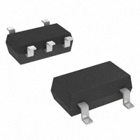
(Top View) A 1 5 Vcc
B2 GND 3 4Y SOT25 / SOT353
N EW PRODUCT
disables the output preventing damaging current backflow when the device is powered down. The gate performs the positive Boolean function:
Y = A •B
Features
• • • • • • • • • • • • •
or
Y = A +B Applications
• • • Voltage Level Shifting General Purpose Logic Wide array of products such as. • • • • • PCs, networking, notebooks, netbooks, PDAs Computer peripherals, hard drives, CD/DVD ROM TV, DVD, DVR, set top box Cell Phones, Personal Navigation / GPS MP3 players ,Cameras, Video Recorders
Wide Supply Voltage Range from 1.65 to 5.5V ± 24mA Output Drive at 3.3V CMOS low power consumption IOFF Supports Partial-Power-Down Mode Operation Inputs accept up to 5.5V ESD Protection Exceeds JESD 22 200-V Machine Model (A115-A) 2000-V Human Body Model (A114-A) Latch-Up Exceeds 100mA per JESD 78, Class II Range of Package Options Direct Interface with TTL Levels SOT25 and SOT353: Assembled with “Green” Molding Compound (no Br, Sb) Lead Free Finish/ RoHS Compliant (Note 1)
Notes:
1. EU Directive 2002/95/EC (RoHS). All applicable RoHS exemptions applied. Please visit our website at http://www.diodes.com/products/lead_free.html.
74LVC1G08
Document number: DS32199 Rev. 1 - 2
1 of 11 www.diodes.com
May 2010
© Diodes Incorporated
�74LVC1G08
SINGLE 2 INPUT POSITIVE AND GATE
Pin Descriptions
Pin Name A B GND Y Vcc Pin NO. 1 2 3 4 5 Data Input Data Input Ground Data Output Supply Voltage Description
N EW PRODUCT
Logic Diagram
A B
1 2
4 Y
Function Table
Inputs A H L X B H X L Output Y H L L
74LVC1G08
Document number: DS32199 Rev. 1 - 2
2 of 11 www.diodes.com
May 2010
© Diodes Incorporated
�74LVC1G08
SINGLE 2 INPUT POSITIVE AND GATE
Absolute Maximum Ratings (Note 2)
Symbol ESD HBM ESD MM VCC VI Vo Vo IIK IOK IO TJ TSTG
Notes:
Description Human Body Model ESD Protection Machine Model ESD Protection Supply Voltage Range Input Voltage Range Voltage applied to output in high impedance or IOFF state Voltage applied to output in high or low state. Input Clamp Current VI
很抱歉,暂时无法提供与“74LVC1G08W5-7”相匹配的价格&库存,您可以联系我们找货
免费人工找货