AH1803
MICROPOWER, ULTRA-SENSITIVE HALL EFFECT SWITCH
Features
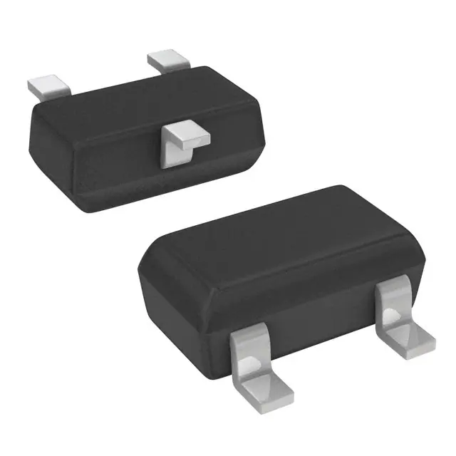
• • • • Micropower operation Operation with North or South Pole 2.4 to 5.5V battery operation Chopper stabilized • Superior temperature stability • Extremely low switch-point drift • Insensitive to physical stress Good RF noise immunity -40°C to 85°C operating temperature Low profile 3 pin SC59 (commonly known as SOT23 in Asia) and DFN2020-6 package ESD (HBM) > 4KV for DFN2020-6 Lead Free Finish / RoHS Compliant (Note 1) Green Packages: SC59 and DFN2020-6
General Description
AH1803 is with two Hall effect plates and a CMOS output driver, mainly designed for battery–operation, hand-held equipment (such as Cellular and Cordless Phone, PDA). The total operation power is down to 24uW in the 3V supply. Either north or south pole of sufficient strength will turn the output on. The output will be turned off under no magnetic field. While the magnetic flux density (B) is larger than operate point (Bop), the output will be turned on (low), the output is held until B is lower than release point (Brp), then turned off (High).
• • • • • •
Applications
• • • Cellular phone PDA Cordless phone
Ordering Information
AH1803 - X X X
Package W : SC59 SN : DFN2020-6
Lead Free G: Green
Packing -7 : Taping
Note:
1. RoHS revision 13.2.2003. Glass and High Temperature Solder Exemptions Applied, see EU Directive Annex Notes 5 and 7.
Device AH1803-W AH1803-SN
Note:
Package Code W SN
Packaging (Note 2) SC59 DFN2020-6
7” Tape and Reel Quantity Part Number Suffix 3000/Tape & Reel -7 3000/Tape & Reel -7
2. Pad layout as shown on Diodes Inc. suggested pad layout document AP02001, which can be found on our website at http://www.diodes.com/datasheets/ap02001.pdf.
AH1803 Rev. 1
1 of 7 www.diodes.com
JULY 2007
© Diodes Incorporated
�AH1803
MICROPOWER, ULTRA-SENSITIVE HALL EFFECT SWITCH
Pin Description
Name Vdd GND Output P/I/O P/I P/I O Pin # 1 2 3 Description Power Supply Input Ground Output Pin
Pin Assignment
SC59 DFN2020-6
3. Output GND 2. 1. Vdd
1. Vdd
NC
3. Output
Top view
NC 2. GND NC
Bottom view
Note: 3. NC is “No Connection”, which is recommended to be tied to ground.
Block Diagram
1
Power switch Offset Cancelling Offset Cancelling Hall Plate Vdd
Amp
Latch
Logical Hall Plate
3
Out
Amp
Latch
2
GND
AH1803 Rev. 1
2 of 7 www.diodes.com
JULY 2007
© Diodes Incorporated
�AH1803
MICROPOWER, ULTRA-SENSITIVE HALL EFFECT SWITCH
Typical Circuit
Vdd
A H 1803 G nd
O u tp u t
Absolute Maximum Ratings
Symbol Vdd B TA Ts PD TJ
(@ TA = 25°C)
Characteristics Supply voltage Magnetic flux density Operating Temperature Range Storage Temperature Range Package Power Dissipation Maximum Junction Temperature (TA = 25°C) SC59 DFN2020-6
Values 7 Unlimited -40 to +85 -65 to +150 230 230 150
Unit V °C °C mW mW °C
Recommended Operating Conditions
Symbol Vdd Parameter Supply Voltage Operating
Conditions
Rating 2.4~5.5
Unit V
AH1803 Rev. 1
3 of 7 www.diodes.com
JULY 2007
© Diodes Incorporated
�AH1803
MICROPOWER, ULTRA-SENSITIVE HALL EFFECT SWITCH
Electrical Characteristics
Symbol Vout Ioff Idd(en) Characteristic Output On Voltage Output Leakage Current
(TA = +25°C, Vdd = 3V; unless otherwise specified)
Conditions Iout =1mA Vout = 5.5V, Brpn < B < Brps Chip enable, TA = 25°C, Vdd = 3V Chip enable, TA = -40~85°C, Vdd = 2.4~5.5V Chip disable, TA = 25°C, Vdd = 3V Chip disable, TA = -40~85°C, Vdd = 2.4~5.5V Average supply current, TA = 25°C, Vdd = 3V Average supply current, TA= -40~85°C, Vdd = 2.4~5.5V
Min -
Typ 0.1
很抱歉,暂时无法提供与“AH1803”相匹配的价格&库存,您可以联系我们找货
免费人工找货