AP1122
1A LOW DROPOUT POSITIVE REGULATOR
Description
AP1122 is a low dropout positive fixed-mode regulator with 1A output current capability. The product is specifically designed to provide well-regulated supply for low voltage IC applications such as high-speed bus termination and low current 1.2V logic supply. AP1122 is also well suited for other applications such as VGA cards. AP1122 is guaranteed to have lower than 1.3V dropout at full load current making it ideal to provide well-regulated outputs of 1.2 output voltage with 2.5V input voltage supply.
Pin Assignments
(Top View)
3 2 1 Tab is VOUT
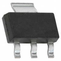
SOT223-3L
VIN VOUT GND
Applications
• • PC peripheral Communication
(Top View)
3 2
VIN
VOUT GND
Features
1
• • • • • • • • • 1.3V maximum dropout at full load current Fixed 1.2V± 2% output voltage Fast transient response Output current limiting Built-in thermal shutdown Good noise rejection Packages: SOT223-3L, TO252-3L, SOT89-3L, TO263-3L and TO220-3L SOT89-3L, SOT223-3L and TO252-3L: Available in “Green” Molding Compound (No Br, Sb) Lead Free Finish/ RoHS Compliant (Note 1)
Tab is VOUT
TO252-3L/ TO263-3L
(Top View)
3 2 1 Tab is VOUT
SOT89-3L
( Top View)
VIN VOUT GND
3 2 1 Tab is VOUT
TO220-3L
Notes: 1. EU Directive 2002/95/EC (RoHS). All applicable RoHS exemptions applied. Please visit our website at http://www.diodes.com/products/lead_free.html. 1 of 11 www.diodes.com
VIN VOUT GND
AP1122
Document number: DS31012 Rev. 9 - 2
May 2010
© Diodes Incorporated
�AP1122
1A LOW DROPOUT POSITIVE REGULATOR Typical Application Circuit
2.5V C1 100uF VIN VOUT GND Tab is VOUT C2 100uF 1.2V/1A
Pin Descriptions
Pin Name GND VOUT I/O I O Pin # 1 2 Ground Pin The output of the regulator. A minimum of 10uF capacitor (0.15Ω ≤ ESR ≤ 20Ω) must be connected from this pin to ground to insure stability. The input pin of regulator. Typically a large storage capacitor is connected from this pin to ground to insure that the input voltage does not sag below the minimum dropout voltage during the load transient response. Description
VIN
I
3
Functional Block Diagram
V IN
3
2
V OUT
+ +
CURRENT LIMIT 1.2V
+
+
Thermal Shutdown 1 GND
AP1122
Document number: DS31012 Rev. 9 - 2
2 of 11 www.diodes.com
May 2010
© Diodes Incorporated
�AP1122
1A LOW DROPOUT POSITIVE REGULATOR Absolute Maximum Ratings
Symbol VIN TST TMJ Parameter DC Supply Voltage Storage Temperature Maximum Junction Temperature Rating -0.3 to 12 -65 to +150 150 Unit V o C o C
Recommended Operating Conditions
Symbol IOUT TOP Parameter Min 0 Max 1.0 125 Unit A o C
Output Current Operating Junction Temperature Range
Electrical Characteristics (Under Operating Conditions)
Parameter
Output Voltage Line Regulation Load Regulation Dropout Voltage (VIN-VOUT) Current Limit Minimum Load Current (Note 4) Thermal Regulation Ripple Rejection Temperature Stability
Test Conditions
2.5V≦VIN≦12V, IO=10mA, TA=25 C 2.5V≦VIN≦12V, IO=10mA, TA=25oC VIN=2.5V~12V, 10mA
很抱歉,暂时无法提供与“AP1122EG-13”相匹配的价格&库存,您可以联系我们找货
免费人工找货