BAV70DW
QUAD SURFACE MOUNT SWITCHING DIODE ARRAY Features
NEW PRODUCT
· · · · ·
Fast Switching Speed Ultra-Small Surface Mount Package For General Purpose Switching Applications High Conductance Two “BAV70” Circuits In One Package
A
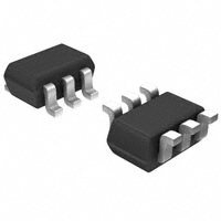
SOT-363 Dim
BC
Min 0.10 1.15 2.00 0.30 1.80 1.80 ¾ 0.90 0.25 0.10 0°
Max 0.30 1.35 2.20 0.40 2.20 2.20 0.10 1.00 0.40 0.25 8°
A B C
Mechanical Data
· · · · · · · Case: SOT-363, Molded Plastic Case Material - UL Flammability Rating Classification 94V-0 Moisture sensitivity: Level 1 per J-STD-020A Terminals: Solderable per MIL-STD-202, Method 208 Orientation: See Diagram Marking: KJA (see page 3) Weight: 0.006 grams (approx.)
K J
G H M
D E G H
D F L
0.65 Nominal
J K L M a
C1
A2
A2
A1
A1
C2
TOP VIEW
All Dimensions in mm
Maximum Ratings @ TA = 25°C unless otherwise specified
Characteristic Non-Repetitive Peak Reverse Voltage Peak Repetitive Reverse Voltage Working Peak Reverse Voltage DC Blocking Voltage RMS Reverse Voltage Forward Continuous Current (Note 1) Average Rectified Output Current (Note 1) Non-Repetitive Peak Forward Surge Current @ t = 1.0ms @ t = 1.0s Power Dissipation (Note 1) Thermal Resistance Junction to Ambient Air (Note 1) Operating and Storage Temperature Range Symbol VRM VRRM VRWM VR VR(RMS) IFM IO IFSM Pd RqJA Tj , TSTG Value 100 75 53 300 150 2.0 1.0 200 625 -65 to +150 Unit V V V mA mA A mW °C/W °C
Electrical Characteristics @ TA = 25°C unless otherwise specified
Characteristic Reverse Breakdown Voltage (Note 2) Symbol V(BR)R VF Min 75 ¾ Max ¾ 0.715 0.855 1.0 1.25 2.5 50 30 25 2.0 4.0 Unit V Test Condition IF = 2.5mA IF = 1.0mA IF = 10mA IF = 50mA IF = 150mA VR = 75V VR = 75V, Tj = 150°C VR = 25V, Tj = 150°C VR = 20V VR = 0, f = 1.0MHz IF = IR = 10mA, Irr = 0.1 x IR, RL = 100W
Forward Voltage (Note 2)
V mA mA mA nA pF ns
Reverse Current (Note 2) Total Capacitance Reverse Recovery Time Notes:
IR CT trr
¾ ¾ ¾
1. Device mounted on FR-4 PCB, 1 inch x 0.85 inch x 0.062 inch; pad layout as shown on Diodes Inc. suggested pad layout document AP02001, which can be found on our website at http://www.diodes.com/datasheets/ap02001.pdf. 2. Short duration test pulse used to minimize self-heating effect.
DS30132 Rev. 4 - 2
1 of 3 www.diodes.com
BAV70DW
�IF, INSTANTANEOUS FORWARD CURRENT (A)
IR, INSTANTANEOUS REVERSE CURRENT (nA)
1
10000
TA = 150ºC TA = 125ºC
NEW PRODUCT
1000
0.1
TA = 150ºC TA = 75ºC TA = 25ºC TA = 0ºC TA = -40ºC
100
TA = 75ºC
10
TA = 25ºC TA = 0ºC
0.01
1
TA = -40ºC
0.001 0 0.5 1.0 1.5 VF, INSTANTANEOUS FORWARD VOLTAGE (V) Fig. 1 Forward Characteristics
2.0 1.8 CT, TOTAL CAPACITANCE (pF) 1.6 1.4 1.2 1.0 0.8 0.6 0.4 0.2 0.0 0 10 20 30 40
Pd, POWER DISSIPATION (mW)
f = 1.0MHz
0.1 0 20 40 60 80 100 VR, INSTANTANEOUS REVERSE VOLTAGE (V) Fig. 2 Typical Reverse Characteristics
300
250
200
150
100
50
0 0 25 50 75 100 125 150
VR, REVERSE VOLTAGE (V) Fig. 3 Typical Capacitance vs. Reverse Voltage
TA, AMBIENT TEMPERATURE (° C) Fig. 4 Power Derating Curve
DS30132 Rev. 4 - 2
2 of 3 www.diodes.com
BAV70DW
�Ordering Information
(Note 3) Packaging SOT-363 Shipping 3000/Tape & Reel
NEW PRODUCT
Device BAV70DW-7 Notes:
3. For Packaging Details, go to our website at http://www.diodes.com/datasheets/ap02007.pdf.
Marking Information
KJA YM KJA YM
Date Code Key Year Code Month Code 2001 M Jan 1 Feb 2 2002 N March 3 2003 P Apr 4 2004 R May 5
KJA = Product Type Marking Code YM = Date Code Marking Y = Year ex: N = 2002 M = Month ex: 9 = September
2005 S Jun 6 Jul 7
2006 T Aug 8
2007 U Sep 9 Oct O
2008 V Nov N
2009 W Dec D
DS30132 Rev. 4 - 2
3 of 3 www.diodes.com
BAV70DW
�
很抱歉,暂时无法提供与“BAV70DW-7”相匹配的价格&库存,您可以联系我们找货
免费人工找货