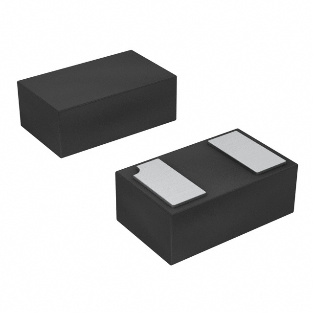
BZT52C5V1LP - BZT52C24LP
SURFACE MOUNT ZENER DIODE
Lead-free Green
SPICE MODELS: BZT52C24LP BZT52C5V1LP BZT52C5V6LP BZT52C6V2LP BZT52C6V8LP BZT52C7V5LP BZT52C8V2LP BZT52C9V1LP BZT52C10LP
BZT52C11LP BZT52C12LP BZT52C13LP BZT52C15LP BZT52C16LP BZT52C18LP BZT52C20LP BZT52C22LP
Features
NEW PRODUCT
• • • •
Ultra-Small Leadless Surface Mount Package Ideally Suited for Automated Assembly Processes Lead Free By Design/RoHS Compliant (Note 1) "Green" Device (Note 2) DFN1006-2
G
H
Dim A B C D G
Min 0.95 0.55 0.45 0.20 0.47 0 0.05
Max 1.075 0.675 0.55 0.30 0.53 0.05 0.15
Typ 1.00 0.60 0.50 0.25 0.50 0.03 0.40 0.10
Mechanical Data
• • • • • • • •
Case: DFN1006-2 Case Material: Molded Plastic, "Green" Molding Compound. UL Flammability Classification Rating 94V-0 Moisture Sensitivity: Level 1 per J-STD-020C Terminal Connections: Cathode Dot (See marking information) Terminals: Finish NiPdAu annealed over Copper leadframe. Solderable per MIL-STD-202, Method 208 Marking: See Electrical Characteristics Table, Dot Denotes Cathode Side (See marking information) Ordering Information: See Page 3 Weight: 0.001 grams
A
B
R
C
H N R
D
N
All Dimensions in mm
Maximum Ratings
Forward Voltage (Note 3)
@ TA = 25°C unless otherwise specified Symbol @ IF = 10mA VF Tj, TSTG Value 0.9 -65 to +150 Unit V °C
Characteristic Operating and Storage Temperature Range
Notes: 1. 2. 3.
No purposefully added lead. Diodes Inc.'s "Green" policy can be found on our website at http://www.diodes.com/products/lead_free/index.php. Short duration pulse test used to minimize self-heating effect.
Thermal Characteristics
Characteristic Power Dissipation
@ TA = 25°C unless otherwise specified Symbol Pd RθJA Value 250 500 Unit mW °C/W
Thermal Resistance, Junction to Ambient Air
DS30506 Rev. 11 - 2
1 of 4 www.diodes.com
BZT52C5V1LP - BZT52C24LP
© Diodes Incorporated
�Electrical Characteristics
@ TA = 25°C unless otherwise specified Maximum Reverse Current (Note 4) IZK mA 480 400 150 80 80 80 100 150 150 150 170 200 200 225 225 250 250 1.0 1.0 1.0 1.0 1.0 1.0 1.0 1.0 1.0 1.0 1.0 1.0 1.0 1.0 1.0 1.0 1.0 IR uA 2.0 1.0 3.0 2.0 1.0 0.7 0.5 0.2 0.1 0.1 0.1 0.1 0.1 0.1 0.1 0.1 0.1 @ VR V 2.0 2.0 4.0 4.0 5.0 5.0 6.0 7.0 8.0 8.0 8.0 10.5 11.2 12.6 14.0 15.4 16.8
NEW PRODUCT
Type Number
Marking Codes
Zener Voltage Range (Note 4) VZ @ IZT Nom (V) 5.1 5.6 6.2 6.8 7.5 8.2 9.1 10 11 12 13 15 16 18 20 22 24 4.8 5.2 5.8 6.4 7.0 7.7 8.5 9.4 10.4 11.4 12.4 13.8 15.3 16.8 18.8 20.8 22.8 5.4 6.0 6.6 7.2 7.9 8.7 9.6 10.6 11.6 12.7 14.1 15.6 17.1 19.1 21.2 23.3 25.6 IZT 5 5 5 5 5 5 5 5 5 5 5 5 5 5 5 5 5
Maximum Zener Impedance (Note 5) ZZT @ IZT ZZK @ IZK Ω 60 40 10 15 15 15 15 20 20 25 30 30 40 45 55 55 70
Typical Temperature Coefficient @ IZTC mV/°C Min -2.7 -2 0.4 1.2 2.5 3.2 3.8 4.5 5.4 6.0 7.0 9.2 10.4 12.4 14.4 16.4 18.4 Max 1.2 2.5 3.7 4.5 5.3 6.2 7.0 8.0 9.0 10.0 11.0 13.0 14.0 16.0 18.0 20.0 22.0
Test Current IZTC mA 5 5 5 5 5 5 5 5 5 5 5 5 5 5 5 5 5
Min (V) Max (V) mA
BZT52C5V1LP BZT52C5V6LP BZT52C6V2LP BZT52C6V8LP BZT52C7V5LP BZT52C8V2LP BZT52C9V1LP BZT52C10LP BZT52C11LP BZT52C12LP BZT52C13LP BZT52C15LP BZT52C16LP BZT52C18LP BZT52C20LP BZT52C22LP BZT52C24LP
Notes:
9Y 9A 9B 9C 9D 9E 9F 9G 9H 9J 9K 9L 9M 9N 9P 9R 9S
4. Short duration test pulse used to minimize self-heating effect. 5. f = 1kHz.
50
Tj = 25°C
30
C5V6LP C6V8LP
Tj = 25°C
C10LP C12LP C15LP
40 IZ, ZENER CURRENT (mA)
C6V2LP C8V2LP
IZ, ZENER CURRENT (mA)
20
30
C18LP
C22LP
20
10
Test current IZ 5mA
10
Test Current IZ 5.0mA
0 0 1 3 4 5 6 8 9 7 VZ, ZENER VOLTAGE (V) Fig. 1 Zener Breakdown Characteristics 2 10
0 0 10 20 VZ, ZENER VOLTAGE (V) Fig. 2 Zener Breakdown Characteristics 30
DS30506 Rev. 11 - 2
2 of 4 www.diodes.com
BZT52C5V1LP - BZT52C24LP
�Ordering Information
(Note 6) Packaging DFN1006-2 Shipping 3000/Tape & Reel
NEW PRODUCT
Device (Type Number)-7*
* Add “-7” to the appropriate type number in Table 1 above example: 6.2V Zener = BZT52C6V2LP-7. Notes: 6. For Packaging Details, go to our website at http://www.diodes.com/datasheets/ap02007.pdf.
Marking Information
9X
9X = Product Type Marking Code, Dot Denotes Cathode Side; See Page 2
Suggested Pad Layout
Dimensions in mm.
1.30 R = 0.05 (8x) 0.30 R = 0.05 (8x)
0.90
0.60 0.70 0.80 (2x) (2x) (2x)
0.30 (2x) 0.40 (2x) 0.50 (2x) solder lands solder resist occupied area solder paste
DS30506 Rev. 11 - 2
3 of 4 www.diodes.com
BZT52C5V1LP - BZT52C24LP
�NEW PRODUCT
IMPORTANT NOTICE Diodes, Inc. and its subsidiaries reserve the right to make changes without further notice to any product herein to make corrections, modifications, enhancements, improvements, or other changes. Diodes, Inc. does not assume any liability arising out of the application or use of any product described herein; neither does it convey any license under its patent rights, nor the rights of others. The user of products in such applications shall assume all risks of such use and will agree to hold Diodes Incorporated and all the companies whose products are represented on our website, harmless against all damages. LIFE SUPPORT The products located on our website at www.diodes.com are not recommended for use in life support systems where a failure or malfunction of the component may directly threaten life or cause injury without the expressed written approval of Diodes Incorporated.
DS30506 Rev. 11 - 2
4 of 4 www.diodes.com
BZT52C5V1LP - BZT52C24LP
�
很抱歉,暂时无法提供与“BZT52C5V1LP-7”相匹配的价格&库存,您可以联系我们找货
免费人工找货- 国内价格
- 5+1.20471
- 50+0.98461
- 150+0.87455
