MMBTA55 / MMBTA56
PNP SMALL SIGNAL SURFACE MOUNT TRANSISTOR
Please click here to visit our online spice models database.
Features
• • • • • Epitaxial Planar Die Construction Complementary NPN Types Available (MMBTA05 / MMBTA06) Ideal for Low Power Amplification and Switching Lead, Halogen and Antimony Free, RoHS Compliant "Green" Device (Notes 3 and 4) Qualified to AEC-Q101 Standards for High Reliability
A C B B E
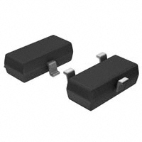
TOP VIEW
SOT-23 Dim
C
Min 0.37 1.20 2.30 0.89 0.45 1.78 2.80 0.013 0.903 0.45 0.085 0°
Max 0.51 1.40 2.50 1.03 0.60 2.05 3.00 0.10 1.10 0.61 0.180 8°
A B C D E G H J K
E
D G H K J L
Mechanical Data
• • • • • • • • • Case: SOT-23 Case Material: Molded Plastic. UL Flammability Classification Rating 94V-0 Moisture Sensitivity: Level 1 per J-STD-020d Terminal Connections: See Diagram Terminals: Solderable per MIL-STD-202, Method 208 Lead Free Plating (Matte Tin Finish annealed over Alloy 42 leadframe). MMBTA55 Marking (See Page 3): K2H, K2G MMBTA56 Marking (See Page 3): K2G Ordering Information: See Page 3 Weight: 0.008 grams (approximate) @TA = 25°C unless otherwise specified
M
C
L M α
All Dimensions in mm
B E
•
Maximum Ratings
Characteristic Collector-Base Voltage Collector-Emitter Voltage Emitter-Base Voltage Collector Current - Continuous (Note 1) Power Dissipation (Note 1) Thermal Resistance, Junction to Ambient (Note 1) Operating and Storage Temperature Range
Symbol VCBO VCEO VEBO IC Pd RθJA Tj, TSTG
MMBTA55 -60 -60 -4.0 -500 300 417
MMBTA56 -80 -80
Unit V V V mA mW °C/W °C
-55 to +150
Electrical Characteristics
Characteristic OFF CHARACTERISTICS (Note 2) Collector-Base Breakdown Voltage Collector-Emitter Breakdown Voltage Emitter-Base Breakdown Voltage Collector Cutoff Current Collector Cutoff Current ON CHARACTERISTICS (Note 2) DC Current Gain Collector-Emitter Saturation Voltage Base-Emitter Saturation Voltage SMALL SIGNAL CHARACTERISTICS Current Gain-Bandwidth Product
@TA = 25°C unless otherwise specified Symbol MMBTA55 MMBTA56 MMBTA55 MMBTA56 MMBTA55 MMBTA56 MMBTA55 MMBTA56 V(BR)CBO V(BR)CEO V(BR)EBO ICBO ICEX Min -60 -80 -60 -80 -4.0 ⎯ ⎯ Max ⎯ ⎯ ⎯ -100 -100 Unit V V V nA nA Test Condition IC = -100μA, IE = 0 IC = -1.0mA, IB = 0 IE = -100μA, IC = 0 VCB = -60V, IE = 0 VCB = -80V, IE = 0 VCE = -60V, IBO = 0V VCE = -80V, IBO = 0V IC = -10mA, VCE = -1.0V IC = -100mA, VCE = -1.0V IC = -100mA, IB = -10mA IC = -100mA, VCE = -1.0V VCE = -1.0V, IC = -100mA, f = 100MHz
hFE VCE(SAT) VBE(SAT) fT
100 ⎯ ⎯ 50
⎯ -0.25 -1.2 ⎯
⎯ V V MHz
Notes: 1. Device mounted on FR-4 PCB, 1 inch x 0.85 inch x 0.062 inch; pad layout as shown on Diodes Inc. suggested pad layout document AP02001, which can be found on our website at http://www.diodes.com/datasheets/ap02001.pdf. 2. Short duration pulse test used to minimize self-heating effect. 3. No purposefully added lead. Halogen and Antimony Free. 4. Product manufactured with Data Code V9 (week 33, 2008) and newer are built with Green Molding Compound. Product manufactured prior to Date Code V9 are built with Non-Green Molding Compound and may contain Halogens or Sb2O3 Fire Retardants.
DS30054 Rev. 11 - 2
1 of 3 www.diodes.com
MMBTA55 / MMBTA56
© Diodes Incorporated
�400 Note 1 350 PD, POWER DISSIPATION (mW) 300 250 200 150 100 50 0 0 25 50 75 100 125 150 175 TA, AMBIENT TEMPERATURE (°C) Fig. 1 Max Power Dissipation vs Ambient Temperature 200
0.25 VCE(SAT), COLLECTOR TO EMITTER SATURATION VOLTAGE (V)
IC IB = 10
0.20 TA = 25°C 0.15
0.10 TA = 150°C 0.05 TA = -50°C
0 1
1,000 100 10 IC, COLLECTOR CURRENT (mA) Fig. 2 Collector Emitter Saturation Voltage vs. Collector Current
1,000 VCE = 5V
1.0 VBE(ON), BASE EMITTER VOLTAGE (V) 0.9 0.8 0.7 0.6 0.5 0.4 0.3 0.2 0.1 0.1 1 10 100 IC, COLLECTOR CURRENT (mA) Fig. 4 Base Emitter Voltage vs. Collector Current TA = 150°C TA = -50°C TA = 25°C VCE = 5V
TA = 150°C hFE, DC CURRENT GAIN
100 TA = 25°C TA = -50°C
10
1
10 1,000 100 IC, COLLECTOR CURRENT (mA) Fig. 3 DC Current Gain vs. Collector Current
100 fT, GAIN-BANDWIDTH PRODUCT (MHz)
VCE = 5V 10
1 10 100 IC, COLLECTOR CURRENT (mA) Fig. 5 Gain-Bandwidth Product vs. Collector Current 1
DS30054 Rev. 11 - 2
2 of 3 www.diodes.com
MMBTA55 / MMBTA56
© Diodes Incorporated
�Ordering Information
Device MMBTA55-7-F MMBTA56-7-F
Notes: 5.
(Note 5) Packaging SOT-23 SOT-23 Shipping 3000/Tape & Reel 3000/Tape & Reel
For packaging details, go to our website at http://www.diodes.com/datasheets/ap02007.pdf.
Marking Information
K2x
K2x = Product Type Marking Code, ex: K2H = MMBTA55 YM = Date Code Marking Y = Year ex: N = 2002 M = Month ex: 9 = September
Date Code Key Year Code Month Code
YM
1998 J Jan 1
1999 K Feb 2
2000 L
2001 M Mar 3
2002 N Apr 4
2003 P May 5
2004 R Jun 6
2005 S
2006 T Jul 7
2007 U Aug 8
2008 V Sep 9
2009 W Oct O
2010 X
2011 Y Nov N
2012 Z Dec D
IMPORTANT NOTICE Diodes Incorporated and its subsidiaries reserve the right to make modifications, enhancements, improvements, corrections or other changes without further notice to any product herein. Diodes Incorporated does not assume any liability arising out of the application or use of any product described herein; neither does it convey any license under its patent rights, nor the rights of others. The user of products in such applications shall assume all risks of such use and will agree to hold Diodes Incorporated and all the companies whose products are represented on our website, harmless against all damages. LIFE SUPPORT Diodes Incorporated products are not authorized for use as critical components in life support devices or systems without the expressed written approval of the President of Diodes Incorporated.
DS30054 Rev. 11 - 2
3 of 3 www.diodes.com
MMBTA55 / MMBTA56
© Diodes Incorporated
�
很抱歉,暂时无法提供与“MMBTA55-7-F”相匹配的价格&库存,您可以联系我们找货
免费人工找货