Lead-free Green
NMSD200B01
200 mA SYNCHRONOUS RECTIFIER FEATURING N-MOSFET AND SCHOTTKY DIODE General Description
NEW PRODUCT
·
NMSD200B01 is best suited for switching voltage regulator and power management applications. It improves efficiency and reliability of DC-DC converters used in Voltage Regulator Modules (VRM) and can support continuous maximum current of 200mA. It features an ESD protected discrete N-MOSFET with low on-resistance and a discrete Schottky diode with low forward drop. It reduces component count, consumes less space and minimizes parastic losses. The component devices can be used as a part of a circuit or as a stand alone discrete device.
6 5 4
1 2 3
Features
· · · · · · · ·
N-MOSFET with ESD Gate Protection N-MOSFET with Low On-Resistance (RDS(ON)) Low Vf Schottky Diode Low Static, Switching and Conduction Losses Good dynamic performance Surface Mount Package Suited for Automated Assembly Lead Free By Design/ROHS Compliant (Note 1) "Green" Device (Note 2)
D_Q1 6
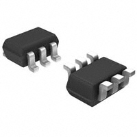
Fig. 1: SOT-363
NC 5
A_D1 4
D DMN601K SD103AWS G Q1
A
D1 SCHOTTKY
Mechanical Data
· · · · · · · ·
Case: SOT-363 Case Material: Molded Plastic. "Green Molding" Compound. UL Flammability Classification Rating 94V-0 Moisture Sensitivity: Level 1 per J-STD-020C Terminal Connections: See Diagram Terminals: Finish - Matte Tin annealed over Alloy 42 leadframe. Solderable per MIL- STD -202, Method 208 Marking & Type Code Information: See Page 7 Ordering Information: See Last Page Weight: 0.016 grams (approximate) Sub-Components DMN601K_DIE (ESD Protected) SD103AWS_DIE Reference Q1 D1
1 G_Q1
NMOS S
C
2 S_Q1
3 C_D1
Fig 2 : Schematic and Pin Configuration
Device Type N-MOSFET Schottky Diode
Figure 2 2
Maximum Ratings, Total Device
Characteristic Power Dissipation (Note 3) Power Derating Factor above 25 °C Output Current
@ TA = 25°C unless otherwise specified Symbol Pd Pder Iout Value 200 1.6 200 Unit mW mW/°C mA
Thermal Characteristics
Characteristic Junction Operation and Storage Temperature Range Thermal Resistance, Junction to Ambient Air (Note 3) (Equivalent to one heated junction of N-MOSFET)
Notes:
Symbol Tj, Tstg RqJA
Value -55 to +150 625
Unit °C °C/W
1. No purposefully added lead. 2 . Diodes Inc.'s "Green" policy can be found on our website at http:/www.diodes.com/products/lead_free/index.php. 3. Device mounted on FR-4 PCB, 1 inch x 0.85 inch x 0.062 inch; pad layout as shown on Diodes Inc. suggested pad layout document AP02001, which can be found on our website at http://www.diodes.com/datasheets/ap02001.pdf.
DS30911 Rev. 2 - 2
1 of 8 www.diodes.com
NMSD200B1
ã Diodes Incorporated
�NEW PRODUCT
Maximum Ratings: @ TA = 25°C unless otherwise specified Sub-Component Device: ESD Protected N-Channel MOSFET (Q1)
Characteristic Drain Source Voltage Drain Gate Voltage (RGS
很抱歉,暂时无法提供与“NMSD200B01-7”相匹配的价格&库存,您可以联系我们找货
免费人工找货