0
登录后你可以
  • 下载海量资料
  • 学习在线课程
  • 观看技术视频
  • 写文章/发帖/加入社区
会员中心
创作中心
发布
  • 发文章

  • 发资料

  • 发帖

  • 提问

  • 发视频

创作活动
SD103CWS-7-F

SD103CWS-7-F

  • 厂商:

    DIODES

  • 封装:

  • 描述:

    SD103CWS-7-F - SURFACE MOUNT SCHOTTKY BARRIER DIODE - Diodes Incorporated

  • 详情介绍
  • 数据手册
  • 价格&库存
SD103CWS-7-F 数据手册
SD103AWS - SD103CWS SURFACE MOUNT SCHOTTKY BARRIER DIODE Please click here to visit our online spice models database. Features • • • • • • • Low Forward Voltage Drop Guard Ring Construction for Transient Protection Negligible Reverse Recovery Time Low Reverse Capacitance Ultra-Small Surface Mount Package Lead, Halogen and Antimony Free, RoHS Compliant "Green" Device (Notes 3 and 4) Qualified to AEC-Q101 Standards for High Reliability (Only for SD103AWS-7-F) Mechanical Data • • • • • • • • • Case: SOD-323 Case Material: Molded Plastic. UL Flammability Classification Rating 94V-0 Moisture Sensitivity: Level 1 per J-STD-020D Leads: Solderable per MIL-STD-202, Method 208 Lead Free Plating (Matte Tin Finish annealed over Alloy 42 leadframe). Polarity: Cathode Band Marking Information: See Page 2 Ordering Information: See Page 2 Weight: 0.004 grams (approximate) Top View Maximum Ratings @TA = 25°C unless otherwise specified Symbol VRRM VRWM VR VR(RMS) IFM IFSM SD103AWS 40 28 SD103BWS 30 21 350 1.5 SD103CWS 20 14 Unit V V mA A Characteristic Peak Repetitive Reverse Voltage Working Peak Reverse Voltage DC Blocking Voltage RMS Reverse Voltage Forward Continuous Current (Note 1) Non-Repetitive Peak Forward Surge Current @ t ≤ 1.0s Thermal Characteristics Characteristic Power Dissipation (Note 1) Thermal Resistance, Junction to Ambient Air (Note 1) Operating and Storage Temperature Range Symbol PD RθJA TJ, TSTG Value 200 625 -65 to +125 Unit mW °C/W °C Electrical Characteristics Characteristic SD103AWS Reverse Breakdown Voltage (Note 2) Forward Voltage Drop SD103AWS Peak Reverse Current (Note 2) Total Capacitance Reverse Recovery Time Notes: 1. 2. 3. 4. @TA = 25°C unless otherwise specified Symbol SD103BWS SD103CWS V(BR)R VF SD103BWS SD103CWS IR CT trr Min 40 30 20 ⎯ ⎯ ⎯ ⎯ Typ ⎯ ⎯ ⎯ 28 10 Max ⎯ 0.37 0.60 5.0 ⎯ ⎯ Unit V V μA pF ns Test Conditions IR = 100μA IR = 100μA IR = 100μA IF = 20mA IF = 200mA VR = 30V VR = 20V VR = 10V VR = 0V, f = 1.0MHz IF = IR = 200mA, Irr = 0.1 x IR, RL = 100Ω Part mounted on FR-4 PC board with recommended pad layout, which can be found on our website at http://www.diodes.com/datasheets/ap02001.pdf. Short duration test pulse used to minimize self-heating effect. No purposefully added lead. Halogen and Antimony Free. Product manufactured with Data Code V9 (week 33, 2008) and newer are built with Green Molding Compound. Product manufactured prior to Date Code V9 are built with Non-Green Molding Compound and may contain Halogens or Sb2O3 Fire Retardants. SD103AWS - SD103CWS Document number: DS30101 Rev. 16 - 2 1 of 3 www.diodes.com July 2008 © Diodes Incorporated SD103AWS - SD103CWS IF, INSTANTANEOUS FORWARD CURRENT (A) 1 1,000 0.1 TA = 125°C T A = 75°C 100 10 0.01 T A = 25°C 1 TA = 0°C 0.001 T A = -40°C 0.1 0.0001 0 200 400 600 800 1,000 VF, INSTANTANEOUS FORWARD VOLTAGE (mV) Fig. 1 Typical Forward Characteristics 30 f = 1.0MHz 0.01 0 15 40 10 20 25 30 5 35 VR, INSTANTANEOUS REVERSE VOLTAGE (V) Fig. 2 Typical Reverse Characteristics PD, POWER DISSIPATION (mW) CT, TOTAL CAPACITANCE (pF) 25 200 20 15 100 10 5 0 0 40 10 30 20 VR, DC REVERSE VOLTAGE (V) Fig. 3 Total Capacitance vs. Reverse Voltage 0 0 25 50 75 100 125 TA, AMBIENT TEMPERATURE (°C) Fig. 4 Power Derating Curve Ordering Information (Note 5) Case SOD-323 SOD-323 SOD-323 Packaging 3000/Tape & Reel 3000/Tape & Reel 3000/Tape & Reel Part Number SD103AWS-7-F SD103BWS-7-F SD103CWS-7-F Notes: 5. For packaging details, go to our website at http://www.diodes.com/datasheets/ap02007.pdf. Marking Information xx = Product Type Marking Code S4 = SD103AWS S5 or S4 = SD103BWS S6 or S5 or S4 = SD103CWS XX SD103AWS - SD103CWS Document number: DS30101 Rev. 16 - 2 2 of 3 www.diodes.com July 2008 © Diodes Incorporated SD103AWS - SD103CWS Package Outline Dimensions C H B A M L K J SOD-323 Dim Min Max A 0.25 0.35 B 1.20 1.40 C 2.30 2.70 H 1.60 1.80 J 0.00 0.10 K 1.0 1.1 L 0.20 0.40 M 0.10 0.15 0° 8° α All Dimensions in mm Suggested Pad Layout C X Dimensions Value (in mm) Z 3.75 G 1.05 X 0.65 Y C Y G Z 1.35 2.40 IMPORTANT NOTICE Diodes Incorporated and its subsidiaries reserve the right to make modifications, enhancements, improvements, corrections or other changes without further notice to any product herein. Diodes Incorporated does not assume any liability arising out of the application or use of any product described herein; neither does it convey any license under its patent rights, nor the rights of others. The user of products in such applications shall assume all risks of such use and will agree to hold Diodes Incorporated and all the companies whose products are represented on our website, harmless against all damages. LIFE SUPPORT Diodes Incorporated products are not authorized for use as critical components in life support devices or systems without the expressed written approval of the President of Diodes Incorporated. SD103AWS - SD103CWS Document number: DS30101 Rev. 16 - 2 3 of 3 www.diodes.com July 2008 © Diodes Incorporated
SD103CWS-7-F
### 物料型号 - SD103AWS - SD103BWS - SD103CWS

### 器件简介 这些型号是表面贴装肖特基势垒二极管,具有低正向电压降、保护瞬态的防护环结构、几乎可以忽略的反向恢复时间和低反向电容等特点。

### 引脚分配 
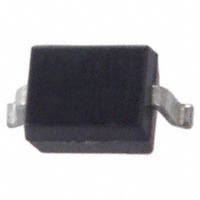
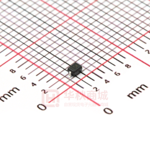
这些二极管为SOD-323封装,具有超小型表面贴装封装,无铅镀层(亚锡表面处理,覆盖在合金42框架上)。

### 参数特性 - 最大额定值:包括峰值重复反向电压、工作峰值反向电压、直流阻断电压、有效值反向电压、正向连续电流、非重复峰值正向浪涌电流等。 - 热特性:包括功率耗散和结到环境空气的热阻。 - 电气特性:包括反向击穿电压、正向电压降、峰值反向电流、总电容和反向恢复时间。

### 功能详解 这些二极管主要用于整流应用,具有低正向电压降和快速反向恢复时间,适用于高频开关应用。

### 应用信息 适用于需要快速开关和低功耗的应用,如电源转换、电机驱动和太阳能光伏系统。

### 封装信息 - 封装类型:SOD-323 - 尺寸:提供了详细的封装尺寸和推荐的焊盘布局。
SD103CWS-7-F 价格&库存

很抱歉,暂时无法提供与“SD103CWS-7-F”相匹配的价格&库存,您可以联系我们找货

免费人工找货
SD103CWS-7-F
    •  国内价格
    • 10+0.23199
    • 100+0.22851
    • 600+0.15585
    • 1200+0.15351
    • 3000+0.1489

    库存:359