SMAJ10CA-13-F

SMAJ10CA-13-F

  • 厂商:

    DIODES

  • 封装:

  • 描述:

    SMAJ10CA-13-F - 400W SURFACE MOUNT TRANSIENT VOLTAGE SUPPRESSOR - Diodes Incorporated

  • 详情介绍
  • 数据手册
  • 价格&库存
SMAJ10CA-13-F 数据手册
SMAJ5.0(C)A - SMAJ170(C)A 400W SURFACE MOUNT TRANSIENT VOLTAGE SUPPRESSOR Features · · · · · · 400W Peak Pulse Power Dissipation Glass Passivated Die Construction Uni- and Bi-Directional Versions Available Excellent Clamping Capability Fast Response Time Lead Free Finish/RoHS Compliant (Note 4) Dim Min 2.29 4.00 1.27 0.15 4.80 0.10 0.76 2.01 Max 2.92 4.60 1.63 0.31 5.59 0.20 1.52 2.30 B SMA A C A B C Mechanical Data · · · · · · · Case: SMA Case Material: Molded Plastic. UL Flammability Classification Rating 94V-0 Moisture Sensitivity: Level 1 per J-STD-020C Terminals: Lead Free Plating (Matte Tin Finish). Solderable per MIL-STD-202, Method 208 Polarity Indicator: Cathode Band (Note: Bi-directional devices have no polarity indicator.) Marking: Date Code and Marking Code See Page 4 Weight: 0.064 grams (approximate) D J D E G H J H G E All Dimensions in mm Maximum Ratings @ TA = 25°C unless otherwise specified Symbol PPK IFSM PM(AV) @ IPP = 35A VF Tj TSTG Value 400 40 1.0 3.5 -55 to +150 -55 to +175 Unit W A W V °C °C Characteristic Peak Pulse Power Dissipation (Non repetitive current pulse derated above TA = 25°C) (Note 1) Peak Forward Surge Current, 8.3ms Single Half Sine Wave Superimposed on Rated Load (JEDEC Method) (Notes 1, 2, & 3) Steady State Power Dissipation @ TL = 75°C Instantaneous Forward Voltage (Notes 1, 2, & 3) Operating Temperature Range Storage Temperature Range Notes: 1. 2. 3. 4. Valid provided that terminals are kept at ambient temperature. Measured with 8.3ms single half sine-wave. Duty cycle = 4 pulses per minute maximum. Unidirectional units only. RoHS revision 13.2.2003. Glass and High Temperature Solder Exemptions Applied, see EU Directive Annex Notes 5 and 7. DS19005 Rev. 13 - 2 1 of 4 www.diodes.com SMAJ5.0(C)A - SMAJ170(C)A ã Diodes Incorporated Part Number Add C For Bi-Directional (Note 5) SMAJ5.0(C)A SMAJ6.0(C)A SMAJ6.5(C)A SMAJ7.0(C)A SMAJ7.5(C)A SMAJ8.0(C)A SMAJ8.5(C)A SMAJ9.0(C)A SMAJ10(C)A SMAJ11(C)A SMAJ12(C)A SMAJ13(C)A SMAJ14(C)A SMAJ15(C)A SMAJ16(C)A SMAJ17(C)A SMAJ18(C)A SMAJ20(C)A SMAJ22(C)A SMAJ24(C)A SMAJ26(C)A SMAJ28(C)A SMAJ30(C)A SMAJ33(C)A SMAJ36(C)A SMAJ40(C)A SMAJ43(C)A SMAJ45(C)A SMAJ48(C)A SMAJ51(C)A SMAJ54(C)A SMAJ58(C)A SMAJ60(C)A SMAJ64(C)A SMAJ70(C)A SMAJ75(C)A SMAJ78(C)A SMAJ85(C)A SMAJ90(C)A SMAJ100(C)A SMAJ110(C)A SMAJ120(C)A SMAJ130(C)A SMAJ150(C)A SMAJ160(C)A SMAJ170(C)A Notes: Reverse Standoff Voltage VRWM (V) 5.0 6.0 6.5 7.0 7.5 8.0 8.5 9.0 10 11 12 13 14 15 16 17 18 20 22 24 26 28 30 33 36 40 43 45 48 51 54 58 60 64 70 75 78 85 90 100 110 120 130 150 160 170 Breakdown Voltage VBR @ IT (Note 6) Min (V) 6.40 6.67 7.22 7.78 8.33 8.89 9.44 10.0 11.1 12.2 13.3 14.4 15.6 16.7 17.8 18.9 20.0 22.2 24.4 26.7 28.9 31.1 33.3 36.7 40.0 44.4 47.8 50.0 53.3 56.7 60.0 64.4 66.7 71.1 77.8 83.3 86.7 94.4 100 111 122 133 144 167 178 189 Max (V) 7.25 7.37 7.98 8.60 9.21 9.83 10.4 11.1 12.3 13.5 14.7 15.9 17.2 18.5 19.7 20.9 22.1 24.5 26.9 29.5 31.9 34.4 36.8 40.6 44.2 49.1 52.8 55.3 58.9 62.7 66.3 71.2 73.7 78.6 86.0 92.1 95.8 104 111 123 135 147 159 185 197 209 Test Current IT (mA) 10 10 10 10 1.0 1.0 1.0 1.0 1.0 1.0 1.0 1.0 1.0 1.0 1.0 1.0 1.0 1.0 1.0 1.0 1.0 1.0 1.0 1.0 1.0 1.0 1.0 1.0 1.0 1.0 1.0 1.0 1.0 1.0 1.0 1.0 1.0 1.0 1.0 1.0 1.0 1.0 1.0 1.0 1.0 1.0 Max. Reverse Leakage @ VRWM (Note 7) IR (mA) 800 800 500 200 100 50 10 5.0 5.0 5.0 5.0 5.0 5.0 5.0 5.0 5.0 5.0 5.0 5.0 5.0 5.0 5.0 5.0 5.0 5.0 5.0 5.0 5.0 5.0 5.0 5.0 5.0 5.0 5.0 5.0 5.0 5.0 5.0 5.0 5.0 5.0 5.0 5.0 5.0 5.0 5.0 Max. Clamping Voltage @ Ipp VC (V) 9.2 10.3 11.2 12.0 12.9 13.6 14.4 15.4 17.0 18.2 19.9 21.5 23.2 24.4 26.0 27.6 29.2 32.4 35.5 38.9 42.1 45.4 48.4 53.3 58.1 64.5 69.4 72.7 77.4 82.4 87.1 93.6 96.8 103 113 121 126 137 146 162 177 193 209 243 259 275 Max. Peak Pulse Current Ipp (A) 43.5 38.8 35.7 33.3 31.0 29.4 27.7 26.0 23.5 22.0 20.1 18.6 17.2 16.4 15.3 14.5 13.7 12.3 11.2 10.3 9.5 8.8 8.3 7.5 6.9 6.2 5.7 5.5 5.2 4.9 4.6 4.3 4.1 3.9 3.5 3.3 2.2 2.9 2.7 2.5 2.3 2.0 1.9 1.6 1.5 1.4 Marking Code BITE TG TK TM TP TR TT TV TX TZ UE UG UK UM UP UR UT UV UX UZ VE VG VK VM VP VR VT VV VX VZ WE WG WK WM WP WR WT WV WX WZ XE XG XK XM XP XR UNIHE HG HK HM HP HR HT HV HX HZ IE IG IK IM IP IR IT IV IX IZ JE JG JK JM JP JR JT JV JX JZ RE RG RK RM RP RR RT RV RX RZ SE SG SK SM SP SR 5. Suffix C denotes Bi-directional device. 6. VBR measured with IT current pulse = 300ms 7. For Bi-Directional devices having VRWM of 10V and under, the I R is doubled. DS19005 Rev. 13 - 2 2 of 4 www.diodes.com SMAJ5.0(C)A - SMAJ170(C)A 100 10000 Tj = 25° C PEAK PULSE DERATING IN % OF PEAK POWER OR CURRENT 75 CT, JUNCTION CAPACITANCE (pF) Unidirectional 1000 50 Bidirectional 100 25 10 X 1000 Waveform as defined by REA 0 0 25 50 75 100 125 150 175 200 TA, AMBIENT TEMPERATURE (° C) Fig. 1 Pulse Derating Curve 100 10 1 10 100 1000 VWM, STANDOFF VOLTAGE (V) Fig. 2 Typical Total Capacitance IP, PEAK PULSE CURRENT (%Ipp) Pd, PEAK PULSE POWER (kW) Tj = 25° C Non Repetitive Pulse Waveform Shown in Fig. 4 100 Peak Value Ipp 10 Half Value Ipp/2 50 1.0 tp 0.1 0.1 1.0 10 100 1000 10000 0 10 X 1000 Waveform as defined by R.E.A. 0 1 2 3 t, TIME (ms) Fig. 4 Pulse Waveform PM(AV), STEADY STATE POWER DISSIPATION (W) 60 1.0 PEAK FORWARD SURGE CURRENT, (A) 50 Pulse Width 8.3ms Single Half-Sine-Wave (JEDEC METHOD) 0.8 40 0.6 30 0.4 20 0.2 60Hz Resistive or Inductive Load 10 0 1 2 5 10 20 50 100 NUMBER OF CYCLES AT 60Hz Fig. 5 Maximum Non-Repetitive Surge Current 0.0 0 25 50 75 100 125 150 175 200 TL, LEAD TEMPERATURE (° C) Fig. 6 Steady State Power Derating Curve DS19005 Rev. 13 - 2 3 of 4 www.diodes.com SMAJ5.0(C)A - SMAJ170(C)A Ordering Information Device (Note 8) Packaging SMA Shipping 5000/Tape & Reel SMAJXXX(C)A-13-F Notes: 8. For Packaging Details, go to our website at http://www.diodes.com/datasheets/ap02007.pdf. *x = Device Voltage, e.g., SMCJ170A-13-F. Example: SMAJ170A-13-F. Marking Information YWW XX XX = Product type marking code (See Page 2) = Manufacturers’ code marking YWW = Date code marking Y = Last digit of year ex: 2 for 2002 WW = Week code 01 to 52 IMPORTANT NOTICE Diodes, Inc. and its subsidiaries reserve the right to make changes without further notice to any product herein to make corrections, modifications, enhancements, improvements, or other changes. Diodes, Inc. does not assume any liability arising out of the application or use of any product described herein; neither does it convey any license under its patent rights, nor the rights of others. The user of products in such applications shall assume all risks of such use and will agree to hold Diodes Incorporated and all the companies whose products are represented on our website, harmless against all damages. LIFE SUPPORT The products located on our website at www.diodes.com are not recommended for use in life support systems where a failure or malfunction of the component may directly threaten life or cause injury without the express written approval of Diodes Incorporated. DS19005 Rev. 13 - 2 4 of 4 www.diodes.com SMAJ5.0(C)A - SMAJ170(C)A
SMAJ10CA-13-F
1. 物料型号: - DIODES SMAJ5.0(C)A - SMAJ170(C)A

2. 器件简介: - 400W表面贴装瞬态电压抑制器,具有400W峰值脉冲功率耗散、玻璃钝化芯片结构、单向和双向版本可选、优秀的钳位能力、快速响应时间、无铅表面处理/符合RoHS标准。
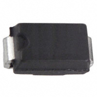
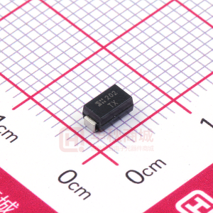
3. 引脚分配: - 封装类型为SMA,具有无铅镀层(亚锡表面处理),符合MIL-STD-202标准方法208的可焊性。阴极带有色环(双向设备没有极性指示)。

4. 参数特性: - 峰值脉冲功率耗散:400W - 峰值正向浪涌电流:40A(8.3ms单半正弦波叠加在额定负载上,JEDEC方法) - 稳态功率耗散:1.0W - 工作温度范围:-55至+150°C - 存储温度范围:-55至+175°C

5. 功能详解: - 该器件主要用于抑制电路中的瞬态电压,保护电路免受电压尖峰的影响。

6. 应用信息: - 适用于需要瞬态电压保护的场合,如电源、通信设备、汽车电子等。

7. 封装信息: - 封装类型为SMA,尺寸参数详细列出了最小值和最大值,所有尺寸单位为毫米。
SMAJ10CA-13-F 价格&库存

很抱歉,暂时无法提供与“SMAJ10CA-13-F”相匹配的价格&库存,您可以联系我们找货

免费人工找货