UMC4N
DUAL COMPLEMENTARY PRE-BIASED TRANSISTORS
Features
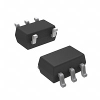
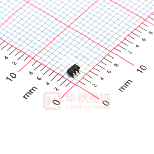
• • • • • Epitaxial Planar Die Construction Surface Mount Package Suited for Automated Assembly Simplifies Circuit Design and Reduces Board Space Lead Free/RoHS Compliant (Note 1) "Green" Device (Note 2) SOT-353
3 2 1
(3) (2) R1 R2 R2 Q1 R1 (5) (1) Q1 R1 = 47kΩ R2 = 47kΩ Q2 R1 = 10kΩ R2 = 47kΩ
N EW PRODUCT
Mechanical Data
• • • • • • • • Case: SOT-353 Case Material: Molded Plastic. UL Flammability Classification Rating 94V-0 Moisture Sensitivity: Level 1 per J-STD-020C Terminal Connections: See Diagram Terminals: Finish – Matte Tin Annealed Over Alloy 42 Leadframe. Solderable per MIL-STD-202, Method 208 Marking Information: See Page 4 Ordering Information: See Page 4 Weight: 0.006 grams (approximate)
4
5
Q2 (4)
TOP VIEW
Schematic and Pin Configuration
Maximum Ratings, Total Device
@TA = 25°C unless otherwise specified Symbol PD RθJA Tj, TSTG Value 150 833 -55 to +150 Unit mW °C/W °C
Characteristic Power Dissipation (Note 3) Thermal Resistance, Junction to Ambient Air (Note 3) Operating and Storage Temperature Range
Maximum Ratings, Pre-Biased NPN Transistor, Q1
Characteristic Supply Voltage Input Voltage Output Current Collector Current
@TA = 25°C unless otherwise specified Value 50 -10 to +40 30 100 Unit V V mA mA
Symbol VCC VIN IO IC(MAX)
Maximum Ratings, Pre-Biased PNP Transistor, Q2
Characteristic Supply Voltage Input Voltage Output Current Collector Current
Notes:
@TA = 25°C unless otherwise specified Value -50 -40 to +6 -100 -100 Unit V V mA mA
Symbol VCC VIN IO IC(MAX)
1. No purposefully added lead. 2. Diodes Inc.'s "Green" policy can be found on our website at http://www.diodes.com/products/lead_free/index.php. 3. Device mounted on FR-4 PCB; pad layout as shown on Diodes Inc. suggested pad layout document AP02001, which can be found on our website at http://www.diodes.com/datasheets/ap02001.pdf.
DS31203 Rev. 3 - 2
1 of 4 www.diodes.com
UMC4N
© Diodes Incorporated
�Electrical Characteristics, Pre-Biased NPN Transistor, Q1 @TA = 25°C unless otherwise specified
Characteristic Input Voltage Output Voltage Input Current Output Current DC Current Gain Gain-Bandwidth Product Input Resistance Resistance Ratio
*Characteristic of Transistor – for reference only.
N EW PRODUCT
Symbol VI(off) VI(on) VO(on) II IO(off) GI fT R1 R2/R1
Min ⎯ 3 ⎯ ⎯ ⎯ 68 ⎯ 32.9 0.8
Typ ⎯ ⎯ 0.1 ⎯ ⎯ ⎯ 250 47 1
Max 0.5 ⎯ 0.3 0.18 0.5 ⎯ ⎯ 61.1 1.2
Unit V V V mA μA ⎯ MHz kΩ ⎯
Test Condition VCC = 5V, IO = 100μA VO = 0.3V, IO = 2mA IO/ II = 10mA/0.5 mA V I = 5V VCC = 50V, VI = 0V VO = 5V, IO = 5mA VCE = 10V, IE = -5mA, f = 100MHz* ⎯ ⎯
Electrical Characteristics, Pre-Biased PNP Transistor, Q2 @TA = 25°C unless otherwise specified
Characteristic Input Voltage Output Voltage Input Current Output Current DC Current Gain Gain-Bandwidth Product Input Resistance Resistance Ratio
*Characteristic of Transistor – for reference only.
Symbol VI(off) VI(on) VO(on) II IO(off) GI fT R1 R2/R1
Min ⎯ -1.4 ⎯ ⎯ ⎯ 68 ⎯ 7 3.7
Typ ⎯ ⎯ -0.1 ⎯ ⎯ ⎯ 250 10 4.7
Max -0.3 ⎯ -0.3 -0.88 -0.5 ⎯ ⎯ 13 5.7
Unit V V V mA μA ⎯ MHz kΩ ⎯
Test Condition VCC = -5V, IO = -100μA VO = -0.3V, IO = -1mA IO/ II = -5mA/-0.25 mA VI = -5V VCC = -50V, VI = 0V VO = -5V, IO = -5mA VCE = -10V, IE = 5mA, f = 100MHz* ⎯ ⎯
1,000
IO/II = 20
100
TA = 150°C
TA = 85°C
TA = 150°C
10
T A = 85°C TA = 25°C T A = -55°C VO = 5V
TA = -55°C TA = 25°C
1 IO, OUTPUT CURRENT (mA) Fig. 1 Typical DC Current Gain vs. Output Current (Q1, NPN)
0.1
1
10
100
DS31203 Rev. 3 - 2
2 of 4 www.diodes.com
UMC4N
© Diodes Incorporated
�10
10
VCC = 5V
N EW PRODUCT
1
TA = -55°C TA = 25°C TA = 85°C TA = 150°C
TA = -55°C
1
T A = 25°C T A = 85°C TA = 150°C
VO = 0.3V
0.1 0.01
0.1
1
10
0.1 0.01
0.1
1
10
100
1
IO/II = 20
TA = 150°C TA = 85°C TA = 25°C T A = -55°C
0.1
T A = 85°C
TA = 150°C
T A = 25°C TA = -55°C
VO = -5V
0.01 0.1 1 10 -IO, OUTPUT CURRENT (mA) Fig. 6 Typical Output Voltage vs. Output Current (Q2, PNP) 100
10
VCC = -5V
10
VO = -0.3V
1
T A = -55°C TA = 25°C TA = 85°C TA = 150°C
1
TA = -55°C T A = 25°C T A = 85°C T A = 150°C
0.1 0.01
0.1
0.1 1 -IO, OUTPUT CURRENT (mA) Fig. 7 Typical Input Off Voltage vs. Output Current (Q2, PNP)
10
-IO, OUTPUT CURRENT (mA) Fig. 8 Typical Input ON Voltage vs. Output Current (Q2, PNP)
DS31203 Rev. 3 - 2
3 of 4 www.diodes.com
UMC4N
© Diodes Incorporated
�Ordering Information (Note 4)
Device UMC4N-7
Notes:
Packaging SOT-353
Shipping 3000/Tape & Reel
4. For packaging details, go to our website at http://www.diodes.com/datasheets/ap02007.pdf.
N EW PRODUCT
Marking Information
NP1
NP1 = Product Type Marking Code YM = Date Code Marking Y = Year ex: U = 2007 M = Month ex: 9 = September
Date Code Key
Year Code Month Code Jan 1
2007 U Feb 2 Mar 3
2008 V Apr 4
YM
2009 W May 5 Jun 6 Jul 7
2010 X Aug 8 Sep 9
2011 Y Oct O Nov N
2012 Z Dec D
Package Outline Dimensions
A
SOT-353 Dim A Min 0.10 1.15 2.00 0.30 1.80 ⎯ 0.90 0.25 0.10 0° Max 0.30 1.35 2.20 0.40 2.20 0.10 1.00 0.40 0.25 8°
TOP VIEW
BC
B C D F
0.65 Nominal
H K M
H J K L M α
J
D
F
L
All Dimensions in mm
IMPORTANT NOTICE Diodes Incorporated and its subsidiaries reserve the right to make modifications, enhancements, improvements, corrections or other changes without further notice to any product herein. Diodes Incorporated does not assume any liability arising out of the application or use of any product described herein; neither does it convey any license under its patent rights, nor the rights of others. The user of products in such applications shall assume all risks of such use and will agree to hold Diodes Incorporated and all the companies whose products are represented on our website, harmless against all damages. LIFE SUPPORT Diodes Incorporated products are not authorized for use as critical components in life support devices or systems without the expressed written approval of the President of Diodes Incorporated.
DS31203 Rev. 3 - 2
4 of 4 www.diodes.com
UMC4N
© Diodes Incorporated
�
很抱歉,暂时无法提供与“UMC4N-7”相匹配的价格&库存,您可以联系我们找货
免费人工找货- 国内价格
- 5+0.57908
- 50+0.4705
- 150+0.41621