BZTW52C2V4 ... BZTW52C75
BZTW52C2V4 ... BZTW52C75
Ptot = 350 mW
VZ
= 2.4 V ... 75 V
Tjmax = 150°C
SMD Planar Zener Diodes
SMD Planar Zener-Dioden
Version 2019-07-26
Typical Applications
Voltage stabilization and regulators
(For overvoltage protection
see TVS diodes SMF series)
Commercial grade 1)
1.1
2.7
0.1
0.6
3.8
Features
Sharp Zener voltage breakdown
Low leakage current
Compliant to RoHS, REACH,
Conflict Minerals 1)
Mechanical Data 1)
Taped and reeled
Weight approx.
Dimensions - Maße [mm]
Type Code:
See table – siehe Tabelle
RoHS
Pb
EE
WE
Type
Code
1.6
0.6
Typische Anwendungen
Spannungsstabilisierung und -regler
(Für Überspannungsschutz
siehe TVS-Diodenreihe SMF)
Standardausführung 1)
EL
V
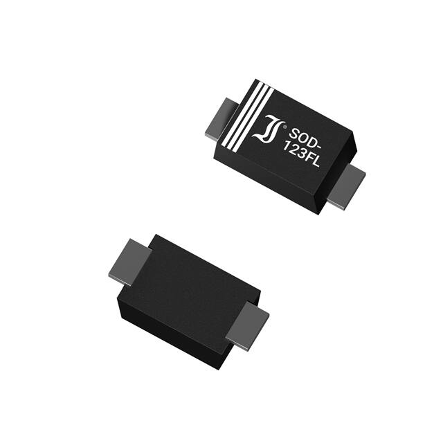
SOD-123
Besonderheiten
Scharfer Zenerspannungsabbruch
Niedriger Sperrstrom
Konform zu RoHS, REACH,
Konfliktmineralien 1)
Mechanische Daten 1)
3000 / 7“
Gegurtet auf Rolle
0.01 g
Gewicht ca.
Case material
UL 94V-0
Gehäusematerial
Solder & assembly conditions
260°C/10s
Löt- und Einbaubedingungen
MSL = 1
Standard Zener voltage tolerance is graded to the international E 24 (~ ±5%) standard. Zener voltages see table on next
page. Other voltage tolerances and higher Zener voltages on request.
Die Toleranz der Zener-Spannung ist in der Standard-Ausführung gestuft nach der internationalen Reihe E 24 (~ ±5%).
Zener-Spannungen siehe Tabelle auf der nächsten Seite. Andere Toleranzen oder höhere Z-Spannungen auf Anfrage.
Maximum ratings 2)
Grenzwerte 2)
Power dissipation
Verlustleistung
Ptot
350 mW 3)
Junction temperature – Sperrschichttemperatur
Storage temperature – Lagerungstemperatur
Tj
TS
-50...+150°C
-50...+125°C
Characteristics
Kennwerte
Typ. thermal resistance junction to ambient
Typ. Wärmewiderstand Sperrschicht-Umgebung
1
2
3
RthA
250 K/W 3)
Please note the detailed information on our website or at the beginning of the data book
Bitte beachten Sie die detaillierten Hinweise auf unserer Internetseite bzw. am Anfang des Datenbuches
TA = 25°C unless otherwise specified – TA = 25°C wenn nicht anders angegeben
Mounted on P.C. board with 25 mm2 copper pads per terminal – Montage auf Leiterplatte mit 25 mm2 Lötpads je Anschluss
© Diotec Semiconductor AG
http://www.diotec.com/
1
�BZTW52C2V4 ... BZTW52C75
Characteristics
(Tj = 25°C unless otherwise specified)
Type
Typ
Code
BZTW52C...
Z-voltage range 1)
Z-Spannungs-Bereich 1)
IZ = 5 mA
VZ min [V]
2
Dynamic resistance
Diff. Widerstand
rzj [Ω] at f = 1 kHz
Temp. Coefficient
of Z-voltage
…der Z-Spannung
Reverse voltage
Sperrspannung
VR at/bei IR
Z-current 2)
Z-Strom 2)
TA = 25°C
VZ max [V]
IZ = 5 mA
αVZ [10-4 /°C]
VR [V]
IR [µA]
IZmax [mA]
-9...-6
2V4
WX
2.28
2.52
< 100
1
50
139
2V7
W1
2.57
2.84
< 100
-9...-6
1
20
123
3V0
W2
2.85
3.15
< 95
-8...-5
1
10
111
3V3
W3
3.14
3.47
< 95
-8...-5
1
5
101
3V6
W4
3.42
3.78
< 90
-8...-5
1
5
93
3V9
W5
3.71
4.10
< 90
-8...-5
1
3
85
4V3
W6
4.09
4.52
< 90
-6...-3
1
3
77
4V7
W7
4.47
4.94
< 80
-5...+2
2
3
71
5V1
W8
4.85
5.36
< 60
-2...+2
2
2
65
5V6
W9
5.32
5.88
< 40
-5...+5
2
1
60
6V2
WA
5.89
6.51
< 10
-3...+6
4
3
54
6V8
WB
6.40
7.20
< 15
+3...+7
4
2
49
7V5
WC
7.10
7.90
< 15
+3...+7
5
1
44
8V2
WD
7.79
8.61
< 15
+8...+7
5
0.7
41
9V1
WE
8.65
9.60
< 15
+3...+9
6
0.5
36
10
WF
9.50
10.50
< 20
+3...+10
7
0.2
33
11
WG
10.45
11.55
< 20
+3...+11
8
0.1
30
12
WH
11.40
12.60
< 25
+3...+11
8
0.1
28
13
WI
12.35
13.65
< 30
+3...+11
8
0.1
26
15
WJ
14.25
15.75
< 30
+3...+11
10.5
0.1
22
16
WK
15.20
16.80
< 40
+3...+11
11
0.1
21
18
WL
17.10
18.90
< 45
+3...+11
12
0.1
19
20
WM
19.00
21.00
< 55
+3...+11
14
0.1
17
22
WN
20.90
23.10
< 55
+4...+12
15
0.1
15
24
WO
22.80
25.20
< 70
+4...+12
16.5
0.1
49
IZ =
1
2
Kennwerte
(Tj = 25°C wenn nicht anders angegeben)
27
WP
30
WQ
33
WR
36
WS
39
WT
43
2 mA
2 mA
28.35
< 80
+4...+12
18.5
0.1
12
28.50
31.50
< 80
+4...+12
21
0.1
11
31.35
34.65
< 80
+4...+12
23
0.1
10
34.20
37.80
< 90
+4...+12
25
0.1
9
37.00
41.00
< 130
+4...+12
27
0.1
9
WU
40.85
45.15
< 150
+4...+12
30
0.05
8
47
WV
44.60
49.40
< 170
+4...+12
36
0.1
7
51
X1
48.40
53.60
< 180
+4...+12
39
0.1
7
56
X2
53.20
58.80
< 200
+4...+12
43
0.1
6
62
X3
58.90
65.10
< 225
+4...+12
47
0.1
5
68
X4
64.60
71.40
< 240
+4...+12
52
0.1
5
75
X5
71.25
78.80
< 265
+4...+12
56
0.1
4
25.65
Tested with pulses (20 ms) – Gemessen mit Impulsen (20 ms)
Mounted on P.C. board with 25 mm2 copper pads per terminal – Montage auf Leiterplatte mit 25 mm2 Lötpad je Anschluss
http://www.diotec.com/
© Diotec Semiconductor AG
�BZTW52C2V4 ... BZTW52C75
120
10 3
[%]
[mA]
100
10 2
80
Tj = 100°C
10
60
Tj = 25°C
40
1
20
IF
Ptot
10
0
0
TA
100
50
150
-1
0
[°C]
VF
0.4
0.6
0.8
1.0
[V] 1.4
Forward characteristics (typical values)
Durchlasskennlinien (typische Werte)
3
Power dissipation versus ambient temperature )
Verlustleistung in Abh. von d. Umgebungstemp.3)
15
5,1
[mA]
5,6
6,2
4,7
10
8,2
6,8
7,5
10
9,1
Tj = 25°C
f = 1.0 MHz
VR = 1V
[pF]
VR = 2V
4,3
VR = 1V
3,9
I Z = 5 mA
5
IZ
3,6
3,3
VR = 2V
3,0
2,7
2,4
2,0
0
0
VZ
2
3
4
5
6
7
8
10
[V]
Zener Voltage vs. Zener current – Abbruchspannung über Zenerstrom
Cj
VZ
[V]
Junction capacitance vs. zener voltage (typical)
Sperrschichtkapazität in Abh. v.d. Zenerspg. (typ.)
10
18
24
30
36
43
51
56
62
68
75
IZmax
Tj = 25°C
Typical breakdown characteristic – tested with pulses
Typische Abbruchspannung – gemessen mit Impulsen
Disclaimer: See data book page 2 or website
Haftungssauschluss: Siehe Datenbuch Seite 2 oder Internet
© Diotec Semiconductor AG
http://www.diotec.com/
3
�
很抱歉,暂时无法提供与“BZTW52C5V6”相匹配的价格&库存,您可以联系我们找货
免费人工找货