DI080N03PQ
DI080N03PQ
ID25°C = 80 A
RDS(on) ~ 1.4 mΩ
Tjmax
= 150°C
N-Channel Power MOSFET
N-Kanal Leistungs-MOSFET
VDSS = 30 V
PD = 35 W
EAS = 150 mJ
Version 2021-09-13
SS
S
Typical Applications
DC/DC Converters
Power Supplies
DC Drives
Power Tools
Synchronous Rectifiers
Commercial grade
Suffix -Q: AEC-Q101 compliant 1)
Suffix -AQ: in AEC-Q101 qualification 1)
G
Typische Anwendungen
Gleichstrom-Wandler
Stromversorgungen
Gleichstrom-Antriebe
Elektrowerkzeuge
Synchrongleichrichter
Standardausführung
Suffix -Q: AEC-Q101 konform 1)
Suffix -AQ: in AEC-Q101 Qualifikation 1)
Features
Low profile, space saving package
Low on state resistance
Fast switching times
Low gate charge
Avalanche rated
Compliant to RoHS (exemp. 7a)
REACH, Conflict Minerals 1)
D
SPICE Model & STEP File 1)
RoHS
EE
WE
Pb
EL
V
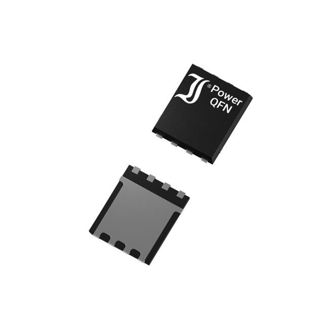
QFN5x6
~TDSON-8 / DFN5060
Mechanical Data 1)
Mechanische Daten 1)
Taped and reeled
5000 / 13“
Weight approx.
Marking Code
503N015
Besonderheiten
Flache, platzsparende Bauform
Niedriger Einschaltwiderstand
Schnelle Schaltzeiten
Niedrige Gate-Ladung
Avalanche-Charakteristik
Konform zu RoHS (Ausn. 7a)
REACH, Konfliktmineralien 1)
Gegurtet auf Rolle
0.1 g
Gewicht ca.
Case material
UL 94V-0
Gehäusematerial
Solder & assembly conditions
260°C/10s
Löt- und Einbaubedingungen
MSL = 1
HS Code 85412100
Maximum ratings 1)
Grenzwerte 2)
DI080N03PQ
Drain-Source voltage
Drain-Source-Spannung
VGS = 0 V (short)
Gate-Source-voltage continuos – Gate-Source-Spannung dauernd
2
VDSS
30 V
VGSS
± 20 V
Power dissipation – Verlustleistung
TC = 25°C )
Ptot
35 W
Drain current continous
Drainstrom dauernd
TC = 25°C 3)
ID
80 A
Drain current continous – Drainstr. dauernd
TC = 100°C 3)
ID
70 A
IDM
160 A
Peak Drain current – Drain-Spitzenstrom
3
)
3
Source current cont. – Sourcestr. dauernd
TC = 25°C )
IS
42 A
Peak Source current – Source-Spitzenstrom
VGS = 0 V, tp = 10 ms
ISM
120 A
VDD = 15 V, VG = 10 V
L = 0.5 mH, RG = 25 Ω
EAS
150 mJ
Tj
TS
-55…+150°C
-55…+150°C
Single pulse avalanche energy
Einzelpuls Avalanche-Energie
(Fig. 1)
Junction temperature – Sperrschichttemperatur
Storage temperature – Lagerungstemperatur
1
1
2
3
Please note the detailed information on our website or at the beginning of the data book
Bitte beachten Sie die detaillierten Hinweise auf unserer Internetseite bzw. am Anfang des Datenbuches
TA = 25°C, unless otherwise specified – TA = 25°C, wenn nicht anders angegeben
Measured at heat flange – Gemessen an der Kühlfahne
Pulse width limited by Tjmax – Pulsbreite begrenzt durch Tjmax
© Diotec Semiconductor AG
http://www.diotec.com/
1
�DI080N03PQ
Characteristics (static)
Kennwerte (statisch)
Tj = 25°C
Min.
Typ.
Max.
V(BR)DSS
30 V
–
–
IDSS
–
–
1 µA
IGSS
–
–
± 100 nA
VGS(th)
1.2 V
–
2.5 V
RDS(on)
–
1.4 mΩ
–
1.8 mΩ
2.5 mΩ
Drain-Source breakdown voltage – Drain-Source-Durchbruchspannung
ID = 250 µA
VGS = 0 V (short)
Drain-Source leakage current – Drain-Source Leckstrom
VDS = 24 V
VGS = 0 V (short)
Gate-Body leakage current – Gate-Substrat Leckstrom
VGS = ±20 V VDS = 0 V (short)
Gate-Source threshold voltage – Gate-Source Schwellspannung
VGS = VDS
ID = 250 µA
Drain-Source on-state resistance – Drain-Source Einschaltwiderstand
VGS = 10 V
VGS = 4.5 V
ID = 30 A
ID = 15 A
Characteristics (dynamic)
Kennwerte (dynamisch)
Tj = 25°C
Min.
Typ.
Max.
gFS
–
61 S
–
Ciss
–
7460 pF
–
Coss
–
890 pF
–
Crss
–
730 pF
–
td(on)
tr
–
43 ns
71 ns
–
td(off)
tf
–
42 ns
12 ns
–
Qg
–
163 nC
–
Qgs
–
23 nC
–
Qgd
–
37 nC
–
RGi
–
0.5 Ω
–
Forward Transconductance – Übertragungssteilheit
VDS = 5 V
ID = 20 A
Input Capacitance – Eingangskapazität
VDS = 15 V
VGS = 0 V
f = 1 MHz
Output Capacitance – Ausgangskapazität
VDS = 15 V
VGS = 0 V
f = 1 MHz
Reverse Transfer Capacitance – Rückwirkungskapazität
VDS = 15 V
VGS = 0 V
f = 1 MHz
Turn-On Delay & Rise Time – Einschaltverzögerung und Anstiegszeit
VDD = 15 V
ID = 30 A
VGS = 10 V
RG = 3.3 Ω
(Fig. 1)
Turn-Off Delay & Fall Time – Ausschaltverzögerung und Abfallzeit
VDD = 15 V
ID = 30 A
VGS = 0 V
RG = 3.3 Ω
(Fig. 1)
Total Gate Charge – Gesamte Gate-Ladung
VDD = 15 V
ID = 30 A
VGS = 10 V
Gate-Source Charge – Gate-Source-Ladung
VDD = 15 V
ID = 30 A
VGS = 10 V
Gate-Drain Charge – Gate-Drain-Ladung
VDD = 15 V
ID = 30 A
VGS = 10 V
Intrinsic Gate resistance – Innerer Gatewiderstand
f = 1 Mhz
D open
Fig. 1
Test circuit for switching
times (R) and avalanche
energy (L)
td(on) tr
(“rise“ und “fall“ beziehen sich auf I D)
2
VDS
90%
VGS
(“rise“ and “fall“ refer to I D )
Testaufbau für Schaltzeiten (R)
und Avalanche-Energie (L)
td(off) tf
VDS
VGS
RG
R
ID
VDD
L
10%
http://www.diotec.com/
© Diotec Semiconductor AG
�DI080N03PQ
Characteristics (diode)
Kennwerte (Diode)
Tj = 25°C
Min.
Typ.
Max.
VSD
–
–
1.2 V
trr
–
27 ns
–
Qrr
–
15 nC
–
Forward voltage – Durchlass-Spannung
VGS = 0 V
IS = 1 A
Reverse recovery time – Sperrverzugszeit
IS = 20 A,
di/dt = -100 A/µs
Reverse recovery charge – Sperrverzugsladung
IS = 20 A,
di/dt = -100 A/µs
Characteristics (thermal)
Kennwerte (thermisch)
Thermal resistance junction to case
Wärmewiderstand Sperrschicht – Gehäuse
Min.
Typ.
Max.
–
3.6 K/W
1
)
–
RthC
Dimensions – Maße [mm]
3
10
100
D = 0.5
[A]
[%]
T j = 1 2 5 °C
102
D = 0.1
10
ZthA
RthA
D -> 0
T j = 2 5 °C
D =t p/T
D = 0.02
0
tp
10
T
1 0.01 [ms]
0.1
1
10
10 2
[tp]
Relative transient thermal impedance vs. pulse duration (typical)
Relativer transienter Wärmewiderstand über Impulsdauer (typisch)
1
10 3
IS
VGS = 0V
10-1
0.4
VSD
0.8
1.0
1.2
1.4
[V] 1.8
Source-Drain diode characteristics (typical values)
Kennlinie der Source-Drain Diode (typische Werte)
Disclaimer: See data book page 2 or website
Haftungssauschluss: Siehe Datenbuch Seite 2 oder Internet
1
Measured towards heat sink area (Drain) – Gemessen zur Kühlfläche (Drain)
© Diotec Semiconductor AG
http://www.diotec.com/
3
�
很抱歉,暂时无法提供与“DI080N03PQ”相匹配的价格&库存,您可以联系我们找货
免费人工找货- 国内价格 香港价格
- 5000+4.411165000+0.57065