LDI1117xxD
LDI1117xxD
Adjustable and Fixed Low Drop Voltage Regulators
Einstellbare und Festspannungs-Low-Drop Regler
VO
= VREF ... 13.65 V
VREF (adj) = 1.25 V ± 1.0%
Tol.
= ± 1.0%
ILIMIT = ~1.35 A
Tjmax = 125°C
Version 2021-09-23
8
1
2
3
7
6
5
4
SPICE Model & STEP File 1)
4
VIN
VOUT
GND
2/3/
6/7
5/8 = NC
Marking
Type/Typ
HS Code 85411000
Typische Anwendungen
Hocheffiziente Linearregler
Aktive SCSI-Abschluss-Regler
Ausgangsregler für getaktete
Gleichstromwandler
Batterie-gestützte Spannungsversorgung
Standardausführung1)
Features
Low Dropout Voltage (LDO):
1.15V at 1A output current
Integrated current limiting and
thermal overload protection
Narrow tolerance band
Adjustable or with fixed voltage:
1.2V, 1.5V, 1.8V, 2.5V, 3.3V, 5.0V
Also available in SOT-89 and
SOT-223 packages
Compliant to RoHS (w/o exemp.)
REACH,Conflict Minerals 1)
RoHS
Pb
EE
WE
1
Typical Applications
High efficiency linear regulators,
Active SCSI termination regulator,
Post regulators for switch mode
DC-DC converters,
Battery backed-up regulated supply
Commercial grade 1)
EL
V
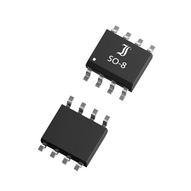
SO-8
Besonderheiten
Niedriger Spannungsabfall (LDO):
1.15V bei 1A Ausgangsstrom
Integrierte Strombegrenzung und
thermische Überlastsicherung
Enge Spannungstoleranz
Einstellbar oder Festspannung:
1.2V, 1.5V, 1.8V, 2.5V, 3.3V, 5.0V
Auch erhältlich im SOT-89 und
SOT-223 Gehäuse
Konform zu RoHS (ohne Ausn.)
REACH, Konfliktmineralien 1)
Mechanical Data 1)
Mechanische Daten 1)
Taped and reeled
4000 / 13“
Weight approx.
Gegurtet auf Rolle
0.08 g
Gewicht ca.
Case material
UL 94V-0
Gehäusematerial
Solder & assembly conditions
260°C/10s
Löt- und Einbaubedingungen
MSL = 3
Maximum ratings 2)
Grenzwerte 2)
Input voltage
Eingangsspannung
VIN
20 V
Power dissipation
Verlustleistung
Ptot
Internally limited 3)
Junction temperature – Sperrschichttemperatur
Storage temperature – Lagerungstemperatur
Tj
TS
+150°C
-55…+150°C
Recommended operating area
Empfohlener Betriebsbereich
Min.
Max.
Input voltage
Eingangsspannung
VIN
-
15 V
Junction temperature
Sperrschichttemperatur
TJ
-40°C
+125°C
1
2
3
Please note the detailed information on our website or at the beginning of the data book
Bitte beachten Sie die detaillierten Hinweise auf unserer Internetseite bzw. am Anfang des Datenbuches
TA = 25°C, unless otherwise specified – TA = 25°C, wenn nicht anders angegeben
The maximum power dissipation at ambient temperature: Ptot = (TJmax – TA)/Rtha
Maximale Verlustleistung bei Umgebungstemperatur: Ptot = (TJmax – TA)/Rtha
© Diotec Semiconductor AG
http://www.diotec.com/
1
�LDI1117xxD
Characteristics 1 )
Kennwerte
LDI1117-ADD
1, 2
Min.
Typ.
Max.
VREF
1.238 V
1.225 V
1.250 V
1.250 V
1.262 V
1.270 V
∆ VOUT
-
0.035%
0.2 %
∆ VOUT
-
0.2 %
0.4 %
-
1.00 V
1.1 V
-
1.08 V
1.18 V
-
1.15 V
1.25 V
1.25 A
1.35 A
-
-
60 µA
120 µA
-
0.2 µA
5 µA
-
1.7 mA
5 mA
IQ
-
5.0 mA
10 mA
VRR
60 dB
75 dB
-
-
0.50%
-
-
0.003 %
-
)
Reference voltage – Referenzspannung
IOUT = 10 mΑ, VIN - VOUT = 2 V
10 mA ≤ IOUT ≤ 1Α, 1.4 V ≤ VIN - VOUT ≤ 8 V
P≤ Maximum Power Dissipation
Line Regulation – Betriebsspannungsdurchgriff
IOUT = 10 mΑ, 1.5 V ≤ VIN - VOUT ≤ 10 V
Load Regulation – Lastregelung
VIN - VOUT = 2 V, 10 mA ≤ IOUT ≤ 1 Α
Dropout Voltage – Spannungsabfall
IOUT = 0.1 Α
IOUT = 0.5 Α
VD
IOUT = 1.0 Α
Current Limit – Grenzstrom
VIN - VOUT = 2 V
ILIMIT
Adjust Pin Current
Adjust Pin Current Change
1.4 V ≤ VIN - VOUT ≤ 10 V, 10 mA ≤ IOUT ≤ 1 Α
Minimum Load Current ( Adjustable only)
1.5 V ≤ VIN - VOUT ≤ 10 V (Adjustable only)
Quiescent current – Ruhestrom
VIN = VOUT + 1.25 V
Ripple Rejection – Störspannungsunterdrückung
IOUT = 1 A, f = 120 Hz, Tj = 25°C
VIN - VOUT = 3V, Vripple = 1Vpp
Temperature Stability – Temperaturstabilität
RMS Output Noise (% of VOUT) – Effektives Ausgangsrauschen
TA = +25°C, 10Hz ≤ f ≤ 10kHz
Typical thermal resistance junction to case
Typischer Wärmewiderstand Sperrschicht – Gehäuse
RthC
15 K/W 2)
Dimensions – Maße [mm]
1
2
2
Tj = 25°C and VIN ≤ 10V, unless otherwise specified – Tj = 25°C und VIN ≤ 10V, wenn nicht anders angegeben
Mounted on P.C. board with 3 mm2 copper pad at each terminal
Montage auf Leiterplatte mit 3 mm2 Kupferbelag (Lötpad) an jedem Anschluss
http://www.diotec.com/
© Diotec Semiconductor AG
�LDI1117xxD
Characteristics 1 )
Kennwerte
LDI1117-1.2D
1, 2
Min.
Typ.
Max.
VOUT
1.176 V
1.152 V
1.2 V
1.2 V
1.224 V
1.248 V
∆ VOUT
-
1 mV
6 mV
∆ VOUT
-
1 mV
10 mV
-
1.00 V
1.1 V
-
1.08 V
1.18 V
-
1.15 V
1.25 V
ILIMIT
1.25 A
1.35 A
-
IQ
-
5.0 mA
10 mA
VRR
60 dB
75 dB
-
-
0.50%
-
-
0.003%
-
)
Output voltage – Ausgangsspannung
IOUT = 10 mΑ, VIN = 3.2 V
10 mA ≤ IOUT ≤ 1Α, 3.0 V ≤ VIN ≤ 10 V
Line Regulation – Betriebsspannungsdurchgriff
IOUT = 10mΑ, 1.5V ≤ VIN - VOUT ≤ 10 V
Load Regulation – Lastregelung
VIN - VOUT = 2 V, 10 mA ≤ IOUT ≤ 1 Α
Dropout Voltage – Spannungsabfall
IOUT = 0.1 Α
VD
IOUT = 0.5 Α
IOUT = 1.0 Α
Current Limit – Grenzstrom
VIN - VOUT = 2 V
Quiescent current – Ruhestrom
VIN = VOUT + 1.25 V
Ripple Rejection – Störspannungsunterdrückung
IOUT = 1 A, f = 120 Hz, Tj = 25°C
VIN - VOUT = 3V, Vripple = 1Vpp
Temperature Stability – Temperaturstabilität
RMS Output Noise (% of VOUT) – Effektives Ausgangsrauschen
TA = +25°C, 10Hz ≤ f ≤ 10kHz
Typical thermal resistance junction to case
Typischer Wärmewiderstand Sperrschicht – Gehäuse
1
2
RthC
15 K/W 2)
Tj = 25°C and VIN ≤ 10V, unless otherwise specified – Tj = 25°C und VIN ≤ 10V, wenn nicht anders angegeben
Mounted on P.C. board with 3 mm2 copper pad at each terminal
Montage auf Leiterplatte mit 3 mm2 Kupferbelag (Lötpad) an jedem Anschluss
© Diotec Semiconductor AG
http://www.diotec.com/
3
�LDI1117xxD
Characteristics 1 )
Kennwerte
LDI1117-1.5D
1, 2
Min.
Typ.
Max.
VOUT
1.485 V
1.470 V
1.5 V
1.5 V
1.515 V
1.530 V
∆ VOUT
-
1 mV
6 mV
∆ VOUT
-
1 mV
10 mV
-
1.00 V
1.1 V
-
1.08 V
1.18 V
-
1.15 V
1.25 V
ILIMIT
1.25 A
1.35 A
-
IQ
-
5.0 mA
10 mA
VRR
60 dB
75 dB
-
-
0.50%
-
-
0.003%
-
)
Output voltage – Ausgangsspannung
IOUT = 10 mΑ, VIN = 3.5 V
10 mA ≤ IOUT ≤ 1Α, 3.0 V ≤ VIN ≤ 10 V
Line Regulation – Betriebsspannungsdurchgriff
IOUT = 10mΑ, 1.5V ≤ VIN - VOUT ≤ 10 V
Load Regulation – Lastregelung
VIN - VOUT = 2 V, 10 mA ≤ IOUT ≤ 1 Α
Dropout Voltage – Spannungsabfall
IOUT = 0.1 Α
VD
IOUT = 0.5 Α
IOUT = 1.0 Α
Current Limit – Grenzstrom
VIN - VOUT = 2 V
Quiescent current – Ruhestrom
VIN = VOUT + 1.25 V
Ripple Rejection – Störspannungsunterdrückung
IOUT = 1 A, f = 120 Hz, Tj = 25°C
VIN - VOUT = 3V, Vripple = 1Vpp
Temperature Stability – Temperaturstabilität
RMS Output Noise (% of VOUT) – Effektives Ausgangsrauschen
TA = +25°C, 10Hz ≤ f ≤ 10kHz
Typical thermal resistance junction to case
Typischer Wärmewiderstand Sperrschicht – Gehäuse
1
2
4
RthC
15 K/W 2)
Tj = 25°C and VIN ≤ 10V, unless otherwise specified – Tj = 25°C und VIN ≤ 10V, wenn nicht anders angegeben
Mounted on P.C. board with 3 mm2 copper pad at each terminal
Montage auf Leiterplatte mit 3 mm2 Kupferbelag (Lötpad) an jedem Anschluss
http://www.diotec.com/
© Diotec Semiconductor AG
�LDI1117xxD
Characteristics 1 )
Kennwerte
LDI1117-1.8D
1, 2
Min.
Typ.
Max.
VOUT
1.782 V
1.746 V
1.8 V
1.8 V
1.818 V
1.854 V
∆ VOUT
-
1 mV
6 mV
∆ VOUT
-
1 mV
10 mV
-
1.00 V
1.1 V
-
1.08 V
1.18 V
-
1.15 V
1.25 V
ILIMIT
1.25 A
1.35 A
-
IQ
-
5.0 mA
10 mA
VRR
60 dB
75 dB
-
-
0.50%
-
-
0.003%
-
)
Output voltage – Ausgangsspannung
IOUT = 10 mΑ, VIN = 3.8 V
10 mA ≤ IOUT ≤ 1Α, 3.2 V ≤ VIN ≤ 10 V
Line Regulation – Betriebsspannungsdurchgriff
IOUT = 10mΑ, 1.5V ≤ VIN - VOUT ≤ 10 V
Load Regulation – Lastregelung
VIN - VOUT = 2 V, 10 mA ≤ IOUT ≤ 1 Α
Dropout Voltage – Spannungsabfall
IOUT = 0.1 Α
VD
IOUT = 0.5 Α
IOUT = 1.0 Α
Current Limit – Grenzstrom
VIN - VOUT = 2 V
Quiescent current – Ruhestrom
VIN = VOUT + 1.25 V
Ripple Rejection – Störspannungsunterdrückung
IOUT = 1 A, f = 120 Hz, Tj = 25°C
VIN - VOUT = 3V, Vripple = 1Vpp
Temperature Stability – Temperaturstabilität
RMS Output Noise (% of VOUT) – Effektives Ausgangsrauschen
TA = +25°C, 10Hz ≤ f ≤ 10kHz
Typical thermal resistance junction to case
Typischer Wärmewiderstand Sperrschicht – Gehäuse
1
2
RthC
15 K/W 2)
Tj = 25°C and VIN ≤ 10V, unless otherwise specified – Tj = 25°C und VIN ≤ 10V, wenn nicht anders angegeben
Mounted on P.C. board with 3 mm2 copper pad at each terminal
Montage auf Leiterplatte mit 3 mm2 Kupferbelag (Lötpad) an jedem Anschluss
© Diotec Semiconductor AG
http://www.diotec.com/
5
�LDI1117xxD
Characteristics 1 )
Kennwerte
LDI1117-2.5D
1, 2
Min.
Typ.
Max.
VOUT
2.475 V
2.450 V
2.5 V
2.5 V
2.525 V
2.550 V
∆ VOUT
-
1 mV
6 mV
∆ VOUT
-
1 mV
10 mV
-
1.00 V
1.1 V
-
1.08 V
1.18 V
-
1.15 V
1.25 V
ILIMIT
1.25 A
1.35 A
-
IQ
-
5.0 mA
10 mA
VRR
60 dB
75 dB
-
-
0.50%
-
-
0.003%
-
)
Output voltage – Ausgangsspannung
IOUT = 10 mΑ, VIN = 4.5 V
10 mA ≤ IOUT ≤ 1Α, 3.9 V ≤ VIN ≤ 10 V
Line Regulation – Betriebsspannungsdurchgriff
IOUT = 10mΑ, 1.5V ≤ VIN - VOUT ≤ 10 V
Load Regulation – Lastregelung
VIN - VOUT = 2 V, 10 mA ≤ IOUT ≤ 1 Α
Dropout Voltage – Spannungsabfall
IOUT = 0.1 Α
IOUT = 0.5 Α
VD
IOUT = 1.0 Α
Current Limit – Grenzstrom
VIN - VOUT = 2 V
Quiescent current – Ruhestrom
VIN = VOUT + 1.25 V
Ripple Rejection – Störspannungsunterdrückung
IOUT = 1 A, f = 120 Hz, Tj = 25°C
VIN - VOUT = 3V, Vripple = 1Vpp
Temperature Stability – Temperaturstabilität
RMS Output Noise (% of VOUT) – Effektives Ausgangsrauschen
TA = +25°C, 10Hz ≤ f ≤ 10kHz
Typical thermal resistance junction to case
Typischer Wärmewiderstand Sperrschicht – Gehäuse
1
2
6
RthC
15 K/W 2)
Tj = 25°C and VIN ≤ 10V, unless otherwise specified – Tj = 25°C und VIN ≤ 10V, wenn nicht anders angegeben
Mounted on P.C. board with 3 mm2 copper pad at each terminal
Montage auf Leiterplatte mit 3 mm2 Kupferbelag (Lötpad) an jedem Anschluss
http://www.diotec.com/
© Diotec Semiconductor AG
�LDI1117xxD
Characteristics 1 )
Kennwerte
LDI1117-3.3D
1, 2
Min.
Typ.
Max.
VOUT
3.267V
3.235 V
3.3 V
3.3 V
3.333 V
3.365 V
∆ VOUT
-
1 mV
6 mV
∆ VOUT
-
1 mV
10 mV
-
1.00 V
1.1 V
-
1.08 V
1.18 V
-
1.15 V
1.25 V
ILIMIT
1.25 A
1.35 A
-
IQ
-
5.0 mA
10 mA
VRR
60 dB
75 dB
-
-
0.50%
-
-
0.003%
-
)
Output voltage – Ausgangsspannung
IOUT = 10 mΑ, VIN = 5.0 V
10 mA ≤ IOUT ≤ 1Α, 4.75 V ≤ VIN ≤ 10 V
Line Regulation – Betriebsspannungsdurchgriff
IOUT = 10mΑ, 1.5V ≤ VIN - VOUT ≤ 10 V
Load Regulation – Lastregelung
VIN - VOUT = 2 V, 10 mA ≤ IOUT ≤ 1 Α
Dropout Voltage – Spannungsabfall
IOUT = 0.1 Α
VD
IOUT = 0.5 Α
IOUT = 1.0 Α
Current Limit – Grenzstrom
VIN - VOUT = 2 V
Quiescent current – Ruhestrom
VIN = VOUT + 1.25 V
Ripple Rejection – Störspannungsunterdrückung
IOUT = 1 A, f = 120 Hz, Tj = 25°C
VIN - VOUT = 3V, Vripple = 1Vpp
Temperature Stability – Temperaturstabilität
RMS Output Noise (% of VOUT) – Effektives Ausgangsrauschen
TA = +25°C, 10Hz ≤ f ≤ 10kHz
Typical thermal resistance junction to case
Typischer Wärmewiderstand Sperrschicht – Gehäuse
1
2
RthC
15 K/W 2)
Tj = 25°C and VIN ≤ 10V, unless otherwise specified – Tj = 25°C und VIN ≤ 10V, wenn nicht anders angegeben
Mounted on P.C. board with 3 mm2 copper pad at each terminal
Montage auf Leiterplatte mit 3 mm2 Kupferbelag (Lötpad) an jedem Anschluss
© Diotec Semiconductor AG
http://www.diotec.com/
7
�LDI1117xxD
Characteristics 1 )
Kennwerte
LDI1117-05D
1, 2
Min.
Typ.
Max.
VOUT
4.950 V
4.900 V
5.0 V
5.0 V
5.050 V
5.100 V
∆ VOUT
-
1 mV
10 mV
∆ VOUT
-
1 mV
15 mV
-
1.00 V
1.1 V
-
1.08 V
1.18 V
-
1.15 V
1.25 V
ILIMIT
1.25 A
1.35 A
-
IQ
-
5.0 mA
10 mA
VRR
60 dB
75 dB
-
-
0.50%
-
-
0.003%
-
)
Output voltage – Ausgangsspannung
IOUT = 10 mΑ, VIN = 7.0 V
10 mA ≤ IOUT ≤ 1Α, 6.5V ≤ VIN ≤ 12 V
Line Regulation – Betriebsspannungsdurchgriff
IOUT = 10mΑ, 1.5V ≤ VIN - VOUT ≤ 10 V
Load Regulation – Lastregelung
VIN - VOUT = 2 V, 10 mA ≤ IOUT ≤ 1 Α
Dropout Voltage – Spannungsabfall
IOUT = 0.1 Α
VD
IOUT = 0.5 Α
IOUT = 1.0 Α
Current Limit – Grenzstrom
VIN - VOUT = 2 V
Quiescent current – Ruhestrom
VIN = VOUT + 1.25 V
Ripple Rejection – Störspannungsunterdrückung
IOUT = 1 A, f = 120 Hz, Tj = 25°C
VIN - VOUT = 3V, Vripple = 1Vpp
Temperature Stability – Temperaturstabilität
RMS Output Noise (% of VOUT) – Effektives Ausgangsrauschen
TA = +25°C, 10Hz ≤ f ≤ 10kHz
Typical thermal resistance junction to case
Typischer Wärmewiderstand Sperrschicht – Gehäuse
RthC
15 K/W 2)
Typical Applications notes
Applikationshinweise
VIN
Fig. 1 Typical Application
circuit for adjustable voltage
regulator
VOUT
ADJ
10µF
22µF
R1
VOut = (1 + R2/R1) VREF
+ IADJ x R2
LDI1117-05
VIN
VOUT
5V at 1A
GND
10µF
Fig. 1 Typische
Anwendungsschaltung für
einen einstellbaren
Spannungsregler
VOut = (1 + R2/R1) VREF
+ IADJ x R2
R2
VIN =7V
Fig. 1 Typical application
circuit for fixed voltage
regulator
VOUT
LDI1117-AD
VIN
22µF
Fig. 1 Typische
Anwendungsschaltung für
Festspannungsregler
Disclaimer: See data book page 2 or website
Haftungssauschluss: Siehe Datenbuch Seite 2 oder Internet
1
2
8
Tj = 25°C and VIN ≤ 10V, unless otherwise specified – Tj = 25°C und VIN ≤ 10V, wenn nicht anders angegeben
Mounted on P.C. board with 3 mm2 copper pad at each terminal
Montage auf Leiterplatte mit 3 mm2 Kupferbelag (Lötpad) an jedem Anschluss
http://www.diotec.com/
© Diotec Semiconductor AG
�