MMBT7002DW
MMBT7002DW
ID
RDS(on)
Tjmax
N-Channel Enhancement Mode FET
N-Kanal FET – Anreicherungstyp
= 115 mA
< 7.5 Ω
= 150°C
VDSS
Ptot
= 60 V
= 200 mW
Version 2021-05-27
6
1
2
5
4
3
SPICE Model & STEP File 1)
Typical Applications
Signal processing
Logic level converter
Drivers
Commercial grade
Suffix -Q: AEC-Q101 compliant 1)
Suffix -AQ: in AEC-Q101 qualification 1)
Halogen
FREE
R oH S
WE
Pb
EE
Features
Dual FET
Two transistors
in one package
Fast switching times
Compliant to RoHS (w/o exemp.)
REACH, Conflict Minerals 1)
Typische Anwendungen
Signalverarbeitung
Pegel-wandler
Treiberstufen
Standardausführung
Suffix -Q: AEC-Q101 konform 1)
Suffix -AQ: in AEC-Q101 Qualifikation 1)
EL
V
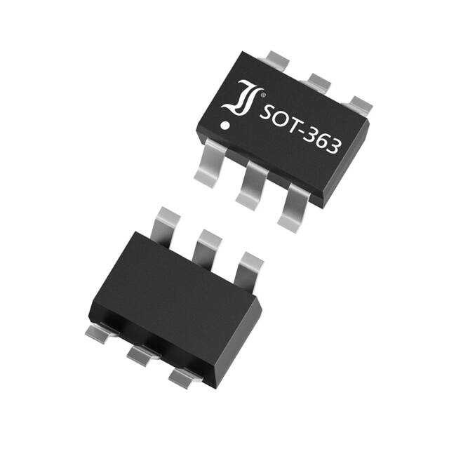
SOT-363
Mechanical Data 1)
Mechanische Daten 1)
Taped and reeled
3000 / 7“
Weight approx.
Marking Code
K72
Besonderheiten
Doppel-MOSFET
Zwei Transistoren
in einem Gehäuse
Schnelle Schaltzeiten
Konform zu RoHS (ohne Ausn.)
REACH, Konfliktmineralien 1)
Gegurtet auf Rolle
0.01 g
Gewicht ca.
Case material
UL 94V-0
Gehäusematerial
Solder & assembly conditions
260°C/10s
Löt- und Einbaubedingungen
MSL = 1
HS Code 85412100
Maximum ratings 1)
Grenzwerte 2)
MMBT7002DW
Drain-Source-voltage – Drain-Source-Spannung
VDSS
60 V
VGSS
± 20 V
Ptot
200 mW 2)
ID
115 mA
Peak Drain current – Drain-Spitzenstrom
IDM
800 mA
Junction temperature – Sperrschichttemperatur
Storage temperature – Lagerungstemperatur
Tj
TS
-55...+150°C
-55…+150°C
Gate-Source-voltage – Gate-Source-Spannung
DC
Power dissipation – Verlustleistung
Drain current – Drainstrom
DC
Dimensions – Maße [mm]
1
1
2
Please note the detailed information on our website or at the beginning of the data book
Bitte beachten Sie die detaillierten Hinweise auf unserer Internetseite bzw. am Anfang des Datenbuches
TA = 25°C, unless otherwise specified – TA = 25°C, wenn nicht anders angegeben
Mounted on P.C. board with 3 mm2 copper pad at each terminal
Montage auf Leiterplatte mit 3 mm2 Kupferbelag (Lötpad) an jedem Anschluss
© Diotec Semiconductor AG
http://www.diotec.com/
1
�MMBT7002DW
Characteristics
Kennwerte
Tj = 25°C
Min.
Typ.
Max.
BVDSS
60 V
–
–
IDSS
–
–
100 nA
±IGSS
–
–
100 nA
VGS(th)
1V
–
2.5 V
RDS(on)
–
–
7.5 Ω
7.5 Ω
gFS
80 mS
–
–
Ciss
–
50 pF
–
Coss
–
25 pF
–
Crss
–
5 pF
–
ton
–
20 ns
–
toff
–
20 ns
–
Drain-Source breakdown voltage – Drain-Source-Durchbruchspannung
ID = 10 µA
Drain-Source leakage current – Drain-Source Leckstrom
VDS = 60 V
VGS = 0 V
Gate-Source leakage current – Gate-Source Leckstrom
VGS = 20 V
Gate-Threshold voltage – Gate-Source Schwellspannung
VGS = VDS = 10 V
ID = 250 µA
Drain-Source on-state resistance – Drain-Source Einschaltwiderstand
VGS = 5 V
VGS = 10 V
ID = 50 mA
ID = 500 mA
Forward Transconductance – Übertragungssteilheit
VDS ≥ 10 VDS(on), ID = 200 mA
Input Capacitance – Eingangskapazität
VDS = 25 V, f = 1 MHz
Output Capacitance – Ausgangskapazität
VDS = 25 V, f = 1 MHz
Reverse Transfer Capacitance – Rückwirkungskapazität
VDS = 25 V, f = 1 MHz
Turn-On Time – Einschaltzeit
VDD= 30 V, RL= 150 Ω, ID= 0.2 A, VGS= 10 V, RG= 25 Ω
Turn-Off Delay Time – Ausschaltverzögerung
VDD= 30 V, RL= 150 Ω, ID= 0.2 A, VGS= 10 V, RG= 25 Ω
Disclaimer: See data book page 2 or website
Haftungssauschluss: Siehe Datenbuch Seite 2 oder Internet
2
http://www.diotec.com/
© Diotec Semiconductor AG
�
很抱歉,暂时无法提供与“MMBT7002DW”相匹配的价格&库存,您可以联系我们找货
免费人工找货- 国内价格 香港价格
- 1+2.005431+0.25807
- 10+1.2486510+0.16069
- 100+0.77684100+0.09997
- 500+0.56927500+0.07326
- 1000+0.501891000+0.06459
- 国内价格 香港价格
- 3000+0.415953000+0.05353
- 6000+0.372526000+0.04794
- 9000+0.350359000+0.04509
- 15000+0.3254315000+0.04188
- 21000+0.3106721000+0.03998
- 30000+0.2963030000+0.03813
- 75000+0.2647575000+0.03407
- 150000+0.24526150000+0.03156
- 300000+0.22913300000+0.02949