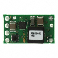
3.3/5/12 Vin Single Output
DC-DC CONVERTERS • • • • • • • • • • • Non-isolated DDR/QDR Memory Bus Termination Module NEW Product 1 VTT bus termination output (output tracks the system VREF) 6 A output current (8 A Peak) 3.3 Vdc, 5 Vdc or 12 Vdc input voltage DDR and QDR compatible ON/OFF inhibit (for VTT standby) Under-voltage lockout Operating temperature range: -40 ºC to +85 ºC Efficiencies up to 88% Output overcurrent protection (non-latching, auto-reset) Point-of-Load-Alliance (POLA) compatible Available RoHS compliant
PTHxx050Y
The PTHxx050Y are a new series of non-isolated dc-dc converters designed specifically for bus termination in DDR and QDR memory applications. Operating from either a 3.3 Vdc, 5 Vdc or 12 Vdc input, the modules generate a VTT output that will source or sink up to 6 A of current to accurately track their VREF input. VTT is the required bus termination supply voltage, and VREF is the reference voltage for the memory and chipset bus receiver comparators. VREF is usually set to half the VDDQ power supply voltage. The PTHxx050Y series employs an actively switched synchronous rectifier output to provide state of the art stepdown switching conversion. The products are small in size and are an ideal choice where space, performance and high efficiency are desired.
All specifications are typical at nominal input, VREF = 1.25 V, full load at 25 °C unless otherwise stated. Cin, Co1 and Co2 = typical value OUTPUT SPECIFICATIONS Output current (over ∆VREF range) Tracking range for VREF Tracking tolerance to VREF (VTT - VREF) (over line, load and temperature) Ripple and noise Load transient response (See Note 5) Output capacitance: Non-ceramic values (See Notes 5 and 6) Ceramic values (See Note 5) (See Note 7) 20 MHz bandwidth All models Continuous (See Note 1) Repetitive pulse (See Note 2) ±6 A ±8 A 0.55-1.8 V -10 mV to +10mV INPUT SPECIFICATIONS CONTD. Input capacitance (See Note 4) Remote ON/OFF GENERAL SPECIFICATIONS Efficiency Io = 4 A Insulation voltage Switching frequency PTH03050Y PTH05050Y PTH12050Y PTH03050Y PTH05050Y PTH12050Y
2 YEAR WARRANTY
SPECIFICATIONS
PTH03050Y and PTH05050Y PTH12050Y
470 µF 560 µF Active high
88% typ. 87% typ. 84% typ. Non-isolated 550- 650 kHz 550-650 kHz 200-300 kHz EN60950 UL/cUL60950 UL94V-0
20 mV pk-pk
80 µs settling time Overshoot/undershoot 25 mV typ. PTH03050Y 470 µF typ., 3,300 µF max. PTH05050Y 470 µF typ., 3,300 µF max. PTH12050Y 940 µF typ., 3,300 µF max. PTH03050Y 200 µF typ., 300 µF max. PTH05050Y 200 µF typ., 300 µF max. PTH12050Y 400 µF typ., 600 µF max. 4 mΩ min ESR (non-ceramic)
Approvals and standards Material flammability Dimensions Weight MTBF Telcordia SR-332 (L x W x H)
22.10 x 12.57 x 8.50 mm 0.870 x 0.495 x 0.335 in 2.9 g (0.10 oz) 6,000,000 hours
INPUT SPECIFICATIONS Input current Input voltage range No load PTH03050Y PTH05050Y PTH12050Y 10 mA 2.95-3.65 Vdc 4.5-5.5 Vdc 10.8-13.2 Vdc ENVIRONMENTAL SPECIFICATIONS Thermal performance (See Note 2) MSL (‘Z’ suffix only) Vin increasing 2.45 V typ., 2.80 V max. Vin decreasing 2.20 V min., 2.40 V typ. Vin Vin Vin Vin increasing 4.30 V typ., 4.45 V max. decreasing 3.40 V min., 3.70 V typ. increasing 9.5 V typ., 10.4 V max. decreasing 8.80 V min., 9.0 V typ. PROTECTION Overcurrent threshold (auto reset) All models 12 A typ. Operating ambient, temperature Non-operating -40 ºC to +85 ºC -40 ºC to +125 ºC
Undervoltage lockout: PTH03050Y PTH05050Y PTH12050Y
JEDEC J-STD-020C Level 3
File Name: PTHxx050Y.pdf Rev (02): 19 Dec 2005
�3.3/5/12 Vin Single Output
DC-DC CONVERTERS Non-isolated DDR/QDR Memory Bus Termination Module NEW Product 2 For the most current data and application support visit www.artesyn.com/powergroup/products.htm
OUTPUT POWER (MAX.) 10.8 W 10.8 W 10.8 W OUTPUT CURRENT (MIN.) 0A 0A 0A OUTPUT CURRENT (MAX.) ±6 A ±6 A ±6 A
PTHxx050Y
VTT RANGE 0.55-1.8Vdc 0.55-1.8Vdc 0.55-1.8Vdc
INPUT VOLTAGE 2.95-3.65 Vdc 4.5-5.5 Vdc 10.8-13.2 Vdc
EFFICIENCY (TYP.) 88% 87% 84%
MODEL NUMBER (9,10) PTH03050Y PTH05050Y PTH12050Y
Part Number System with Options
PTH05050YAST
Packaging Options No Suffix = Trays T = Tape and Reel (8) Mounting Option (9) D = Horizontal Through-Hole (Matte Sn) H = Horizontal Through-Hole (Sn/Pb) S = Surface-Mount (63/37 Sn/Pb pin solder material) Z = Surface-Mount (96.5/3.0/0.5 Sn/Ag/Cu pin solder material) Pin Option A = Through-Hole Std. Pin Length (0.140”) A = Surface-Mount Tin/Lead Solder Ball Output Voltage Code Y = DDR Module
Product Family Point of Load Alliance Compatible Input Voltage 03 = 3.3 V, 05 = 5 V and 12 = 12 V Output Current 05 = 6 A Mechanical Package Always 0
Notes
1 Rating is conditional on the module being directly soldered to a 4 layer PCB with 1 oz. copper. See the SOA curves or contact the factory for appropriate derating. The PTH03050Y and PTH05050Y require no derating up to 85 °C operating temperature and natural convection airflow. Up to 10 ms pulse period at 10% maximum duty. This control pin has an internal pull-up to the input voltage Vin. If it is left open-circuit the module will operate when input power is applied. A small low-leakage (
很抱歉,暂时无法提供与“PTH05050YAS”相匹配的价格&库存,您可以联系我们找货
免费人工找货