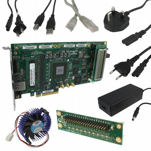
Arria II GX FPGA Development Kit, 6G Edition User
Guide
Arria II GX FPGA Development Kit, 6G Edition
User Guide
101 Innovation Drive
San Jose, CA 95134
www.altera.com
UG-01084-1.0
Subscribe
�Copyright © 2010 Altera Corporation. All rights reserved. Altera, The Programmable Solutions Company, the stylized Altera logo, and specific device designations
are trademarks and/or service marks of Altera Corporation in the U.S. and other countries. All other words and logos identified as trademarks and/or service marks
are the property of Altera Corporation or their respective owners. Altera products are protected under numerous U.S. and foreign patents and pending applications,
maskwork rights, and copyrights. Altera warrants performance of its semiconductor products to current specifications in accordance with Altera's standard
warranty, but reserves the right to make changes to any products and services at any time without notice. Altera assumes no responsibility or liability arising out of
the application or use of any information, product, or service described herein except as expressly agreed to in writing by Altera. Altera customers are advised to
obtain the latest version of device specifications before relying on any published information and before placing orders for products or services.
Arria II GX FPGA Development Kit, 6G Edition User Guide
July 2010 Altera Corporation
�Contents
Chapter 1. About This Kit
Introduction . . . . . . . . . . . . . . . . . . . . . . . . . . . . . . . . . . . . . . . . . . . . . . . . . . . . . . . . . . . . . . . . . . . . . . . . . . . . 1–1
Kit Features . . . . . . . . . . . . . . . . . . . . . . . . . . . . . . . . . . . . . . . . . . . . . . . . . . . . . . . . . . . . . . . . . . . . . . . . . . . . 1–1
Hardware . . . . . . . . . . . . . . . . . . . . . . . . . . . . . . . . . . . . . . . . . . . . . . . . . . . . . . . . . . . . . . . . . . . . . . . . . . . . 1–1
Software . . . . . . . . . . . . . . . . . . . . . . . . . . . . . . . . . . . . . . . . . . . . . . . . . . . . . . . . . . . . . . . . . . . . . . . . . . . . . 1–2
Quartus II Subscription Edition Software . . . . . . . . . . . . . . . . . . . . . . . . . . . . . . . . . . . . . . . . . . . . . . 1–2
Arria II GX FPGA Development Kit, 6G Edition Installer . . . . . . . . . . . . . . . . . . . . . . . . . . . . . . . . . 1–3
Chapter 2. Getting Started
Introduction . . . . . . . . . . . . . . . . . . . . . . . . . . . . . . . . . . . . . . . . . . . . . . . . . . . . . . . . . . . . . . . . . . . . . . . . . . . . 2–1
Before You Begin . . . . . . . . . . . . . . . . . . . . . . . . . . . . . . . . . . . . . . . . . . . . . . . . . . . . . . . . . . . . . . . . . . . . . . . . 2–1
Inspect the Board . . . . . . . . . . . . . . . . . . . . . . . . . . . . . . . . . . . . . . . . . . . . . . . . . . . . . . . . . . . . . . . . . . . . . 2–1
References . . . . . . . . . . . . . . . . . . . . . . . . . . . . . . . . . . . . . . . . . . . . . . . . . . . . . . . . . . . . . . . . . . . . . . . . . . . . . . 2–2
Chapter 3. Software Installation
Introduction . . . . . . . . . . . . . . . . . . . . . . . . . . . . . . . . . . . . . . . . . . . . . . . . . . . . . . . . . . . . . . . . . . . . . . . . . . . . 3–1
Installing the Quartus II Subscription Edition Software . . . . . . . . . . . . . . . . . . . . . . . . . . . . . . . . . . . . . . . 3–1
Licensing Considerations . . . . . . . . . . . . . . . . . . . . . . . . . . . . . . . . . . . . . . . . . . . . . . . . . . . . . . . . . . . . . . 3–1
Installing the Arria II GX FPGA Development Kit, 6G Edition . . . . . . . . . . . . . . . . . . . . . . . . . . . . . . . . . 3–2
Installing the USB-Blaster Driver . . . . . . . . . . . . . . . . . . . . . . . . . . . . . . . . . . . . . . . . . . . . . . . . . . . . . . . . . . 3–3
Chapter 4. Development Board Setup
Introduction . . . . . . . . . . . . . . . . . . . . . . . . . . . . . . . . . . . . . . . . . . . . . . . . . . . . . . . . . . . . . . . . . . . . . . . . . . . . 4–1
Setting Up the Board . . . . . . . . . . . . . . . . . . . . . . . . . . . . . . . . . . . . . . . . . . . . . . . . . . . . . . . . . . . . . . . . . . . . . 4–1
Factory Default Switch Settings . . . . . . . . . . . . . . . . . . . . . . . . . . . . . . . . . . . . . . . . . . . . . . . . . . . . . . . . . . . 4–2
Chapter 5. Board Update Portal
Introduction . . . . . . . . . . . . . . . . . . . . . . . . . . . . . . . . . . . . . . . . . . . . . . . . . . . . . . . . . . . . . . . . . . . . . . . . . . . . 5–1
Connecting to the Board Update Portal Web Page . . . . . . . . . . . . . . . . . . . . . . . . . . . . . . . . . . . . . . . . . . . 5–1
Using the Board Update Portal to Update User Designs . . . . . . . . . . . . . . . . . . . . . . . . . . . . . . . . . . . . . . 5–2
Chapter 6. Board Test System
Introduction . . . . . . . . . . . . . . . . . . . . . . . . . . . . . . . . . . . . . . . . . . . . . . . . . . . . . . . . . . . . . . . . . . . . . . . . . . . . 6–1
Preparing the Board . . . . . . . . . . . . . . . . . . . . . . . . . . . . . . . . . . . . . . . . . . . . . . . . . . . . . . . . . . . . . . . . . . . . . 6–3
Running the Board Test System . . . . . . . . . . . . . . . . . . . . . . . . . . . . . . . . . . . . . . . . . . . . . . . . . . . . . . . . . . . 6–3
Using the Board Test System . . . . . . . . . . . . . . . . . . . . . . . . . . . . . . . . . . . . . . . . . . . . . . . . . . . . . . . . . . . . . . 6–4
The Configure Menu . . . . . . . . . . . . . . . . . . . . . . . . . . . . . . . . . . . . . . . . . . . . . . . . . . . . . . . . . . . . . . . . . . 6–4
The Config Tab . . . . . . . . . . . . . . . . . . . . . . . . . . . . . . . . . . . . . . . . . . . . . . . . . . . . . . . . . . . . . . . . . . . . . . . 6–4
Board Information . . . . . . . . . . . . . . . . . . . . . . . . . . . . . . . . . . . . . . . . . . . . . . . . . . . . . . . . . . . . . . . . . . 6–4
MAX II Registers . . . . . . . . . . . . . . . . . . . . . . . . . . . . . . . . . . . . . . . . . . . . . . . . . . . . . . . . . . . . . . . . . . . 6–5
JTAG Chain Devices . . . . . . . . . . . . . . . . . . . . . . . . . . . . . . . . . . . . . . . . . . . . . . . . . . . . . . . . . . . . . . . . 6–6
Flash Memory Map . . . . . . . . . . . . . . . . . . . . . . . . . . . . . . . . . . . . . . . . . . . . . . . . . . . . . . . . . . . . . . . . . 6–6
The GPIO Tab . . . . . . . . . . . . . . . . . . . . . . . . . . . . . . . . . . . . . . . . . . . . . . . . . . . . . . . . . . . . . . . . . . . . . . . . 6–7
Character LCD . . . . . . . . . . . . . . . . . . . . . . . . . . . . . . . . . . . . . . . . . . . . . . . . . . . . . . . . . . . . . . . . . . . . . 6–7
User DIP Switches . . . . . . . . . . . . . . . . . . . . . . . . . . . . . . . . . . . . . . . . . . . . . . . . . . . . . . . . . . . . . . . . . . 6–7
User LEDs . . . . . . . . . . . . . . . . . . . . . . . . . . . . . . . . . . . . . . . . . . . . . . . . . . . . . . . . . . . . . . . . . . . . . . . . . 6–8
Push Button Switches . . . . . . . . . . . . . . . . . . . . . . . . . . . . . . . . . . . . . . . . . . . . . . . . . . . . . . . . . . . . . . . 6–8
The SRAM&Flash Tab . . . . . . . . . . . . . . . . . . . . . . . . . . . . . . . . . . . . . . . . . . . . . . . . . . . . . . . . . . . . . . . . . 6–8
July 2010 Altera Corporation
Arria II GX FPGA Development Kit, 6G Edition User Guide
�iv
Contents
SRAM . . . . . . . . . . . . . . . . . . . . . . . . . . . . . . . . . . . . . . . . . . . . . . . . . . . . . . . . . . . . . . . . . . . . . . . . . . . . . 6–9
Flash . . . . . . . . . . . . . . . . . . . . . . . . . . . . . . . . . . . . . . . . . . . . . . . . . . . . . . . . . . . . . . . . . . . . . . . . . . . . . . 6–9
The DDR3 Tab . . . . . . . . . . . . . . . . . . . . . . . . . . . . . . . . . . . . . . . . . . . . . . . . . . . . . . . . . . . . . . . . . . . . . . . 6–10
Start . . . . . . . . . . . . . . . . . . . . . . . . . . . . . . . . . . . . . . . . . . . . . . . . . . . . . . . . . . . . . . . . . . . . . . . . . . . . . 6–10
Stop . . . . . . . . . . . . . . . . . . . . . . . . . . . . . . . . . . . . . . . . . . . . . . . . . . . . . . . . . . . . . . . . . . . . . . . . . . . . . 6–10
Performance Indicators . . . . . . . . . . . . . . . . . . . . . . . . . . . . . . . . . . . . . . . . . . . . . . . . . . . . . . . . . . . . . 6–10
Error Control . . . . . . . . . . . . . . . . . . . . . . . . . . . . . . . . . . . . . . . . . . . . . . . . . . . . . . . . . . . . . . . . . . . . . 6–11
Number of Addresses to Write and Read . . . . . . . . . . . . . . . . . . . . . . . . . . . . . . . . . . . . . . . . . . . . . 6–11
Data Type . . . . . . . . . . . . . . . . . . . . . . . . . . . . . . . . . . . . . . . . . . . . . . . . . . . . . . . . . . . . . . . . . . . . . . . . 6–11
Read and Write Control . . . . . . . . . . . . . . . . . . . . . . . . . . . . . . . . . . . . . . . . . . . . . . . . . . . . . . . . . . . . 6–11
The DDR2 Tab . . . . . . . . . . . . . . . . . . . . . . . . . . . . . . . . . . . . . . . . . . . . . . . . . . . . . . . . . . . . . . . . . . . . . . . 6–12
Start . . . . . . . . . . . . . . . . . . . . . . . . . . . . . . . . . . . . . . . . . . . . . . . . . . . . . . . . . . . . . . . . . . . . . . . . . . . . . 6–12
Stop . . . . . . . . . . . . . . . . . . . . . . . . . . . . . . . . . . . . . . . . . . . . . . . . . . . . . . . . . . . . . . . . . . . . . . . . . . . . . 6–12
Performance Indicators . . . . . . . . . . . . . . . . . . . . . . . . . . . . . . . . . . . . . . . . . . . . . . . . . . . . . . . . . . . . . 6–12
Error Control . . . . . . . . . . . . . . . . . . . . . . . . . . . . . . . . . . . . . . . . . . . . . . . . . . . . . . . . . . . . . . . . . . . . . 6–13
Number of Addresses to Write and Read . . . . . . . . . . . . . . . . . . . . . . . . . . . . . . . . . . . . . . . . . . . . . 6–13
Data Type . . . . . . . . . . . . . . . . . . . . . . . . . . . . . . . . . . . . . . . . . . . . . . . . . . . . . . . . . . . . . . . . . . . . . . . . 6–13
Read and Write Control . . . . . . . . . . . . . . . . . . . . . . . . . . . . . . . . . . . . . . . . . . . . . . . . . . . . . . . . . . . . 6–13
The HSMC Tab . . . . . . . . . . . . . . . . . . . . . . . . . . . . . . . . . . . . . . . . . . . . . . . . . . . . . . . . . . . . . . . . . . . . . . 6–14
Status . . . . . . . . . . . . . . . . . . . . . . . . . . . . . . . . . . . . . . . . . . . . . . . . . . . . . . . . . . . . . . . . . . . . . . . . . . . . 6–14
Data Type . . . . . . . . . . . . . . . . . . . . . . . . . . . . . . . . . . . . . . . . . . . . . . . . . . . . . . . . . . . . . . . . . . . . . . . . 6–15
Error Control . . . . . . . . . . . . . . . . . . . . . . . . . . . . . . . . . . . . . . . . . . . . . . . . . . . . . . . . . . . . . . . . . . . . . 6–15
Start . . . . . . . . . . . . . . . . . . . . . . . . . . . . . . . . . . . . . . . . . . . . . . . . . . . . . . . . . . . . . . . . . . . . . . . . . . . . . 6–15
Stop . . . . . . . . . . . . . . . . . . . . . . . . . . . . . . . . . . . . . . . . . . . . . . . . . . . . . . . . . . . . . . . . . . . . . . . . . . . . . 6–15
Performance Indicators . . . . . . . . . . . . . . . . . . . . . . . . . . . . . . . . . . . . . . . . . . . . . . . . . . . . . . . . . . . . . 6–15
The Power Monitor . . . . . . . . . . . . . . . . . . . . . . . . . . . . . . . . . . . . . . . . . . . . . . . . . . . . . . . . . . . . . . . . . . . . . 6–16
General Information . . . . . . . . . . . . . . . . . . . . . . . . . . . . . . . . . . . . . . . . . . . . . . . . . . . . . . . . . . . . . . . 6–17
Power Information . . . . . . . . . . . . . . . . . . . . . . . . . . . . . . . . . . . . . . . . . . . . . . . . . . . . . . . . . . . . . . . . . 6–18
Power Graph . . . . . . . . . . . . . . . . . . . . . . . . . . . . . . . . . . . . . . . . . . . . . . . . . . . . . . . . . . . . . . . . . . . . . 6–18
Graph Settings . . . . . . . . . . . . . . . . . . . . . . . . . . . . . . . . . . . . . . . . . . . . . . . . . . . . . . . . . . . . . . . . . . . . 6–18
Reset . . . . . . . . . . . . . . . . . . . . . . . . . . . . . . . . . . . . . . . . . . . . . . . . . . . . . . . . . . . . . . . . . . . . . . . . . . . . . 6–18
Calculating Power . . . . . . . . . . . . . . . . . . . . . . . . . . . . . . . . . . . . . . . . . . . . . . . . . . . . . . . . . . . . . . . . . . . 6–18
Configuring the FPGA Using the Quartus II Programmer . . . . . . . . . . . . . . . . . . . . . . . . . . . . . . . . . . . . 6–19
Appendix A. Programming the Flash Memory Device
Introduction . . . . . . . . . . . . . . . . . . . . . . . . . . . . . . . . . . . . . . . . . . . . . . . . . . . . . . . . . . . . . . . . . . . . . . . . . . .
CFI Flash Memory Map . . . . . . . . . . . . . . . . . . . . . . . . . . . . . . . . . . . . . . . . . . . . . . . . . . . . . . . . . . . . . . . . .
Preparing Design Files for Flash Programming . . . . . . . . . . . . . . . . . . . . . . . . . . . . . . . . . . . . . . . . . . . . .
Creating Flash Files Using the Nios II EDS . . . . . . . . . . . . . . . . . . . . . . . . . . . . . . . . . . . . . . . . . . . . . .
Programming Flash Memory Using the Board Update Portal . . . . . . . . . . . . . . . . . . . . . . . . . . . . . . . . .
Programming Flash Memory Using the Nios II EDS . . . . . . . . . . . . . . . . . . . . . . . . . . . . . . . . . . . . . . . . .
Restoring the Flash Device to the Factory Settings . . . . . . . . . . . . . . . . . . . . . . . . . . . . . . . . . . . . . . . . . .
Restoring the MAX II CPLD to the Factory Settings . . . . . . . . . . . . . . . . . . . . . . . . . . . . . . . . . . . . . . . . .
A–1
A–1
A–2
A–2
A–3
A–3
A–4
A–5
Additional Information
Document Revision History . . . . . . . . . . . . . . . . . . . . . . . . . . . . . . . . . . . . . . . . . . . . . . . . . . . . . . . . . . . Info–1
How to Contact Altera . . . . . . . . . . . . . . . . . . . . . . . . . . . . . . . . . . . . . . . . . . . . . . . . . . . . . . . . . . . . . . . . Info–1
Typographic Conventions . . . . . . . . . . . . . . . . . . . . . . . . . . . . . . . . . . . . . . . . . . . . . . . . . . . . . . . . . . . . . Info–1
Arria II GX FPGA Development Kit, 6G Edition User Guide
July 2010 Altera Corporation
�1. About This Kit
Introduction
The Altera® Arria® II GX FPGA Development Kit, 6G Edition is a complete design
environment that includes both the hardware and software you need to develop
Arria II GX FPGA designs. The PCI-SIG-compliant board and the one-year license for
the Quartus® II software provide everything you need to begin developing custom
Arria II GX FPGA designs. The following list describes what you can accomplish with
the kit:
■
Develop and test PCI Express® (PCIe) designs
■
Develop and test memory subsystems consisting of DDR2 and DDR3 memories
■
Take advantage of the modular and scalable design by using the high-speed
mezzanine card (HSMC) connectors to interface to over 20 different HSMCs
provided by Altera partners, supporting protocols such as Serial RapidIO®,
10 Gigabit Ethernet, SONET, Common Public Radio Interface (CPRI), Open Base
Station Architecture Initiative (OBSAI) and others
■
Develop FPGAs design for cost-sensitive applications
■
Measure the FPGA's low power consumption
Kit Features
This section briefly describes the Arria II GX FPGA Development Kit, 6G Edition
contents.
Hardware
The Arria II GX FPGA Development Kit, 6G Edition includes the following hardware:
■
Arria II GX FPGA development board, 6G edition—A development platform that
allows you to develop and prototype hardware designs running on the Arria II GX
EP2AGX260 FPGA.
f For detailed information about the board components and interfaces, refer
to the Arria II GX FPGA Development Board, 6G Edition Reference Manual.
■
July 2010 Altera Corporation
Power supply and cables—The kit includes the following items:
■
Power supply and AC adapters for North America/Japan, Europe, and the
United Kingdom
■
USB cable
■
Ethernet cable
Arria II GX FPGA Development Kit, 6G Edition User Guide
�1–2
Chapter 1: About This Kit
Kit Features
Software
The software for this kit, described in the following sections, is available on the Altera
website for immediate downloading. You can also request to have Altera mail the
software to you on DVDs.
Quartus II Subscription Edition Software
The Quartus II Subscription Edition Software is a licensed set of Altera tools with full
functionality. Your kit includes a development kit edition (DKE) license for the
Quartus II software (Windows platform only). This license entitles you to all the
features of the subscription edition for a period of one year. After the year, you must
purchase a renewal subscription to continue using the software. For more
information, refer to the Altera website (www.altera.com).
f Download the Quartus II Subscription Edition Software from the Quartus II
Subscription Edition Software page of the Altera website. Alternatively, you can
request a DVD from the Altera IP and Software DVD Request Form page of the Altera
website.
The Quartus II Subscription Edition Software includes the following items:
■
Quartus II Software—The Quartus II software, including the SOPC Builder system
development tool, provides a comprehensive environment for
system-on-a-programmable-chip (SOPC) design. The Quartus II software
integrates into nearly any design environment and provides interfaces to
industry-standard EDA tools.
f The kit includes a development kit edition (DKE) license for the Quartus II
software (Windows platform only). This license entitles you to all the
features of the subscription edition for a period of one year. After the year,
you must purchase a renewal subscription to continue using the software.
For more information, refer to the Altera website (www.altera.com).
■
MegaCore® IP Library—A library that contains Altera IP MegaCore functions. You
can evaluate MegaCore functions by using the OpenCore Plus feature to do the
following:
■
Simulate behavior of a MegaCore function within your system
■
Verify functionality of your design, and quickly and easily evaluate its size and
speed
■
Generate time-limited device programming files for designs that include
MegaCore functions
■
Program a device and verify your design in hardware
1
The OpenCore Plus hardware evaluation feature is an evaluation tool for
prototyping only. You must purchase a license to use a MegaCore function
in production.
f For more information about OpenCore Plus, refer to OpenCore Plus
Evaluation of Megafunctions.
Arria II GX FPGA Development Kit, 6G Edition User Guide
July 2010 Altera Corporation
�Chapter 1: About This Kit
Kit Features
1–3
■
Nios® II Embedded Design Suite (EDS)—A full-featured set of tools that allow you
to develop embedded software for the Nios II processor which you can include in
your Altera FPGA designs.
Arria II GX FPGA Development Kit, 6G Edition Installer
The license-free Arria II GX FPGA Development Kit, 6G Edition installer includes all
the documentation and design examples for the kit.
Download the Arria II GX FPGA Development Kit, 6G Edition installer from the
Arria II GX FPGA Development Kit, 6G Edition page of the Altera website.
Alternatively, you can request a development kit DVD from the Altera Kit
Installations DVD Request Form page of the Altera website.
July 2010 Altera Corporation
Arria II GX FPGA Development Kit, 6G Edition User Guide
�1–4
Arria II GX FPGA Development Kit, 6G Edition User Guide
Chapter 1: About This Kit
Kit Features
July 2010 Altera Corporation
�2. Getting Started
Introduction
The remaining chapters in this user guide lead you through the following Arria II GX
FPGA development board, 6G edition setup steps:
■
Inspecting the contents of the kit
■
Installing the design and kit software
■
Setting up, powering up, and verifying correct operation of the FPGA
development board, 6G edition
■
Configuring the Arria II GX FPGA
■
Running the Board Test System designs
f For complete information about the FPGA development board, 6G edition, refer to the
Arria II GX FPGA Development Board, 6G Edition Reference Manual.
Before You Begin
Before using the kit or installing the software, check the kit contents and inspect the
board to verify that you received all of the items listed in “Kit Features” on page 1–1.
If any of the items are missing, contact Altera before you proceed.
Inspect the Board
To inspect the board, perform the following steps:
1. Place the board on an anti-static surface and inspect it to ensure that it has not been
damaged during shipment.
c
Without proper anti-static handling, you can damage the board.
2. Verify that all components are on the board and appear intact.
1
In typical applications with the Arria II GX FPGA development board, 6G edition, a
heat sink is not necessary. However, under extreme conditions or for engineering
sample silicon the board might require additional cooling to stay within operating
temperature guidelines. The board has two holes near the FPGA that accommodate
many different heat sinks, including the Dynatron V31G. You can perform power
consumption and thermal modeling to determine whether your application requires
additional cooling. For information about measuring board and FPGA temperature in
real time, refer to “The Power Monitor” on page 6–16.
f For more information about power consumption and thermal modeling, refer to
Thermal Management for FPGAs.
July 2010 Altera Corporation
Arria II GX FPGA Development Kit, 6G Edition User Guide
�2–2
Chapter 2: Getting Started
References
References
Use the following links to check the Altera website for other related information:
■
For the latest board design files and reference designs, refer to the Arria II GX
FPGA Development Kit, 6G Edition page.
■
For additional daughter cards available for purchase, refer to the Development
Board Daughtercards page.
■
For the Arria II GX device documentation, refer to the Literature: Arria II GX
Devices page.
■
To purchase devices from the eStore, refer to the Devices page.
■
For Arria II GX OrCAD symbols, refer to the Capture CIS Symbols page.
■
For Nios II 32-bit embedded processor solutions, refer to the Embedded
Processing page.
Arria II GX FPGA Development Kit, 6G Edition User Guide
July 2010 Altera Corporation
�3. Software Installation
Introduction
This section explains how to install the following software:
■
Quartus II Subscription Edition Software
■
Arria II GX FPGA Development Kit, 6G Edition
■
USB-Blaster™ driver
Installing the Quartus II Subscription Edition Software
The Quartus II Subscription Edition Software provides the necessary tools used for
developing hardware and software for Altera FPGAs. Included in the Quartus II
Subscription Edition Software are the Quartus II software, the Nios II EDS, and the
MegaCore IP Library. The Quartus II software (including SOPC Builder) and the
Nios II EDS are the primary FPGA development tools used to create the reference
designs in this kit. To install the Altera development tools, perform the following
steps:
1. Run the Quartus II Subscription Edition Software installer you acquired in
“Software” on page 1–2.
2. Follow the on-screen instructions to complete the installation process.
f If you have difficulty installing the Quartus II software, refer to Altera Software
Installation and Licensing.
Licensing Considerations
Purchasing this kit entitles you to a one-year DKE license for the Quartus II
Subscription Edition Software. Before using the Quartus II software, you must
activate your license, identify specific users and computers, and obtain and install a
license file.
If you already have a licensed version of the subscription edition, you can use that
license file with this kit. If not, you need to obtain and install a license file. To begin,
go to the Self Service Licensing Center page of the Altera website, log into or create
your myAltera account, and take the following actions:
1. On the Activate Products page, enter the serial number provided with your
development kit in the License Activation Code box.
July 2010 Altera Corporation
Arria II GX FPGA Development Kit, 6G Edition User Guide
�3–2
Chapter 3: Software Installation
Installing the Arria II GX FPGA Development Kit, 6G Edition
1
Your serial number is printed on the development kit box below the bottom
bar code. The number is 10 or 11 alphanumeric characters and does not
contain hyphens. Figure 3–2 shows the correct serial number as
3S150SPXXXX.
Figure 3–1. Locating Your Serial Number
2. Consult the Activate Products table, to determine how to proceed.
a. If the administrator listed for your product is someone other than you, skip the
remaining steps and contact your administrator to become a licensed user.
b. If the administrator listed for your product is you, proceed to the next step.
c. If the administrator listed for your product is Stocking, activate the product,
making you the administrator, and proceed to the next step.
3. Use the Create New License page to license your product for a specific user (you)
on specific computers. The Manage Computers and Manage Users pages allow
you to add users and computers not already present in the licensing system.
1
To license the Quartus II software, you need your computer’s network
interface card (NIC) ID, a number that uniquely identifies your computer.
On the computer you use to run the Quartus II software, type ipconfig
/all at a command prompt to determine the NIC ID. Your NIC ID is the 12digit hexadecimal number on the Physical Address line.
4. When licensing is complete, Altera emails a license.dat file to you. Store the file on
your computer and use the License Setup page of the Options dialog box in the
Quartus_II software to enable the software.
f For complete licensing details, refer to Altera Software Installation and Licensing.
Installing the Arria II GX FPGA Development Kit, 6G Edition
To install the Arria II GX FPGA Development Kit, 6G Edition, perform the following
steps:
1. Run the Arria II GX FPGA Development Kit, 6G Edition installer you acquired in
“Software” on page 1–2.
Arria II GX FPGA Development Kit, 6G Edition User Guide
July 2010 Altera Corporation
�Chapter 3: Software Installation
Installing the USB-Blaster Driver
3–3
2. Follow the on-screen instructions to complete the installation process. Be sure that
the installation directory you choose is in the same relative location to your
Quartus II software as the default locations.
The installation program creates the Arria II GX FPGA Development Kit, 6G Edition
directory structure shown in Figure 3–2.
Figure 3–2. Arria II GX FPGA Development Kit, 6G Edition Installed Directory Structure (1)
The default Windows installation directory is C:\altera\\.
kits
arriaIIGX_2agx260_fpga
board_design_files
demos
documents
examples
factory_recovery
Note to Figure 3–2:
(1) Early-release versions might have slightly different directory names.
Table 3–1 lists the file directory names and a description of their contents.
Table 3–1. Installed Directory Contents
Directory Name
Description of Contents
board_design_files
Contains schematic, layout, assembly, and bill of material board design files. Use these files as a
starting point for a new prototype board design.
demos
Contains demonstration applications.
documents
Contains the kit documentation.
examples
Contains the sample design files for the Arria II GX FPGA Development Kit, 6G Edition.
factory_recovery
Contains the original data programmed onto the board before shipment. Use this data to restore
the board with its original factory contents.
Installing the USB-Blaster Driver
The Arria II GX FPGA development board, 6G edition includes integrated
USB-Blaster circuitry for FPGA programming. However, for the host computer and
board to communicate, you must install the USB-Blaster driver on the host computer.
f Installation instructions for the USB-Blaster driver for your operating system are
available on the Altera website. On the Altera Programming Cable Driver Information
page of the Altera website, locate the table entry for your configuration and click the
link to access the instructions.
July 2010 Altera Corporation
Arria II GX FPGA Development Kit, 6G Edition User Guide
�3–4
Arria II GX FPGA Development Kit, 6G Edition User Guide
Chapter 3: Software Installation
Installing the USB-Blaster Driver
July 2010 Altera Corporation
�4. Development Board Setup
Introduction
The instructions in this chapter explain how to set up the Arria II GX FPGA
development board, 6G edition.
Setting Up the Board
To prepare and apply power to the board, perform the following steps:
1. The Arria II GX FPGA development board, 6G edition ships with its board
switches preconfigured to support the design examples in the kit. If you suspect
your board might not be currently configured with the default settings, follow the
instructions in “Factory Default Switch Settings” on page 4–2 to return the board
to its factory settings before proceeding.
2. The FPGA development board, 6G edition ships with design examples stored in
the flash memory device. Verify the USR LOAD switch (SW4.4) is set to the off
position to load the design stored in the factory portion of flash memory.
Figure 4–1 shows the switch location on the Arria II GX FPGA development
board, 6G edition.
3. Connect the DC adapter (+16 V, 3.75 A) to the DC power jack (J4) on the FPGA
board and plug the cord into a power outlet.
c
Use only the supplied power supply. Power regulation circuitry on the
board can be damaged by power supplies with greater voltage.
4. Set the POWER switch (SW1) to the on position. When power is supplied to the
board, a blue LED (D18) illuminates indicating that the board has power.
The MAX II device on the board contains (among other things) a parallel flash loader
(PFL) megafunction. When the board powers up, the PFL reads a design from flash
memory and configures the FPGA. The USR LOAD switch (SW4.4) controls which
design to load. When the switch is in the off position, the PFL loads the design from
the factory portion of flash memory. When the switch is in the on position, the PFL
loads the design from the user hardware 1 portion of flash memory.
1
The kit includes a MAX II design which contains the MAX II PFL megafunction. The
design resides in the \kits\arriaIIGX_2agx260_fpga\examples\max2
directory.
When configuration is complete, the CONF DONE LED (D14) illuminates, signaling
that the Arria II GX device configured successfully.
f For more information about the PFL megafunction, refer to Using the Parallel Flash
Loader with the Quartus II Software.
July 2010 Altera Corporation
Arria II GX FPGA Development Kit, 6G Edition User Guide
�4–2
Chapter 4: Development Board Setup
Factory Default Switch Settings
Factory Default Switch Settings
This section shows the factory switch settings for the Arria II GX FPGA development
board, 6G edition. Figure 4–1 shows the switch locations and the default position of
each switch on the top side of the board.
Figure 4–1. Switch Locations and Default Settings on the Board Top
User
DIP Switch
ON = 0
OFF = 1
1 2 3 4
SW2
(not installed)
(installed)
(installed)
(installed)
ON
PCIe MODE
DIP Switch
ON
J9
JTAG Control
Jumpers
Board Settings
DIP Switch
ON = 0
OFF = 1
1 2 3 4 5 6 7 8
SW4
ON
1 2 3 4
SW3
To restore the switches to their factory default settings, perform the following steps:
1. Set DIP switch bank (SW3) to match Table 4–1 and Figure 4–1.
Table 4–1. SW3 Dip Switch Settings
Switch
Board
Label
Default
Position
Function
Switch 1 has the following options:
1
PCIe MODE
■
When on, the PCIe card PRSNT2_x1 signal is connected to PCIe card
PRSNT1 signal.
■
When off, the PCIe card PRSNT2_x1 signal floats.
On
Switch 2 has the following options:
2
PCIe MODE
■
When on, the PCIe card PRSNT2_x4 signal is connected to PCIe card
PRSNT1 signal.
■
When off, the PCIe card PRSNT2_x4 signal floats.
On
Switch 3 has the following options:
3
PCIe MODE
■
When on, the PCIe card PRSNT2_x8 signal is connected to PCIe card
PRSNT1 signal.
■
When off, the PCIe card PRSNT2_x8 signal floats.
On
Switch 4 has the following options:
4
PCIe MODE
■
When on, the switch is ignored. It is not connected.
■
When off, the switch is ignored. It is not connected.
Arria II GX FPGA Development Kit, 6G Edition User Guide
Off
July 2010 Altera Corporation
�Chapter 4: Development Board Setup
Factory Default Switch Settings
4–3
2. Set DIP switch bank (SW4) to match Table 4–2 and Figure 4–1.
Table 4–2. SW4 Dip Switch Settings
Board
Label
Switch
Default
Position
Function
Switch 1 has the following options:
1
DIP0
■
When on, reserved.
■
When off, reserved.
Off
Switch 2 has the following options:
2
DIP1
■
When on, reserved.
■
When off, reserved.
Off
Switch 3 has the following options:
3
DIP2
■
When on, reserved.
■
When off, reserved.
Off
Switch 4 has the following options:
4
USR LOAD
■
When on, the PFL loads the user hardware 1 design on power up.
■
When off, the PFL loads the factory design on power up.
Off
Switch 5 has the following options:
5
PWR MON
■
When on, reserved.
■
When off, reserved.
Off
Switch 6 has the following options:
6
USB DISn
■
When on, reserved.
■
When off, reserved.
Off
Switch 7 has the following options:
7
CLK EN
■
When on, all on-board oscillators are enabled.
■
When off, on-board oscillators to the FPGA are disabled.
On
Switch 8 has the following options:
8
CLK SEL
■
When on, programmable oscillator clock (U30) is selected.
■
When off, LVPECL SMA clock (J10 and J11) is selected.
On
3. Set the board jumpers to match Table 4–3 and Figure 4–1.
Table 4–3. JTAG Chain Jumper Settings (Part 1 of 2)
Board
Reference
Board
Label
Default
Shunt Position
Function
This jumper has the following options:
■
J9 pins 1-2
MAX DIS
■
Installing the shunt removes the MAX II EPM2210 device from the
JTAG chain.
Not installed
Removing the shunt includes the MAX II EPM2210 device in the
JTAG chain.
This jumper has the following options:
J9 pins 3-4
HSMA DIS
July 2010 Altera Corporation
■
Installing the shunt removes HSMC port A from the JTAG chain.
■
Removing the shunt includes HSMC port A in the JTAG chain.
Installed
Arria II GX FPGA Development Kit, 6G Edition User Guide
�4–4
Chapter 4: Development Board Setup
Factory Default Switch Settings
Table 4–3. JTAG Chain Jumper Settings (Part 2 of 2)
Board
Reference
Board
Label
Default
Shunt Position
Function
This jumper has the following options:
J9 pins 5-6
HSMB DIS
■
Installing the shunt removes HSMC port B from the JTAG chain.
■
Removing the shunt includes HSMC port B in the JTAG chain.
Installed
This jumper has the following options:
J9 pins 7-8
PCIe DIS
■
Installing the shunt removes the PCIe device from the JTAG chain.
■
Removing the shunt includes the PCIe device in the JTAG chain.
Installed
f For more information about the FPGA board settings, refer to the Arria II GX FPGA
Development Board, 6G Edition Reference Manual.
Arria II GX FPGA Development Kit, 6G Edition User Guide
July 2010 Altera Corporation
�5. Board Update Portal
Introduction
The Arria II GX FPGA Development Kit, 6G Edition ships with the Board Update
Portal design example stored in the factory portion of the flash memory on the board.
The design consists of a Nios II embedded processor, an Ethernet MAC, and an
HTML web server.
When you power up the board with the USR LOAD switch (SW4.4) in the off position,
the Arria II GX FPGA configures with the Board Update Portal design example. The
design can obtain an IP address from any DHCP server and serve a web page from the
flash on your board to any host computer on the same network. The web page allows
you to upload new FPGA designs to the user hardware 1 portion of flash memory,
and provides links to useful information on the Altera website, including links to
kit-specific and design resources.
1
After successfully updating the user hardware 1 flash memory, you can load the user
design from flash memory into the FPGA. To do so, set the USR LOAD switch (SW4.4)
to the on position and power cycle the board.
The source code for the Board Update Portal design resides in the \kits\arriaIIGX_2agx260_fpga\examples directory. If the Board Update Portal is
corrupted or deleted from the flash memory, refer to “Restoring the Flash Device to
the Factory Settings” on page A–4 to restore the board with its original factory
contents.
Connecting to the Board Update Portal Web Page
This section provides instructions to connect to the Board Update Portal web page.
1
Before you proceed, ensure that you have the following:
■
A PC with a connection to a working Ethernet port on a DHCP enabled network.
■
A separate working Ethernet port connected to the same network for the board.
■
The Ethernet and power cables that are included in the kit.
To connect to the Board Update Portal web page, perform the following steps:
1. With the board powered down, set the USR LOAD switch (SW4.4) to the off
position.
2. Attach the Ethernet cable from the board to your LAN.
3. Power up the board. The board connects to the LAN’s gateway router, and obtains
an IP address. The LCD on the board displays the IP address.
4. Launch a web browser on a PC that is connected to the same network, and enter
the IP address from the LCD into the browser address bar. The Board Update
Portal web page appears in the browser.
July 2010 Altera Corporation
Arria II GX FPGA Development Kit, 6G Edition User Guide
�5–2
Chapter 5: Board Update Portal
Using the Board Update Portal to Update User Designs
5. Click Arria II GX FPGA Development Kit, 6G Edition on the Board Update
Portal web page to access the kit’s home page. Visit this page occasionally for
documentation updates and additional new designs.
f You can also navigate directly to the Arria II GX FPGA Development Kit, 6G Edition
page of the Altera website to determine if you have the latest kit software.
Using the Board Update Portal to Update User Designs
The Board Update Portal allows you to write new designs to the user hardware 1
portion of flash memory. Designs must be in the Nios II Flash Programmer File
(.flash) format.
1
Design files available from the Arria II GX FPGA Development Kit, 6G Edition page
of the Altera website include .flash files. You can also create .flash files from your
own custom design. Refer to “Preparing Design Files for Flash Programming” on
page A–2 for information about preparing your own design for upload.
To upload a design over the network into the user portion of flash memory on your
board, perform the following steps:
1. Perform the steps in “Connecting to the Board Update Portal Web Page” to access
the Board Update Portal web page.
2. In the Hardware File Name field specify the .flash file that you either downloaded
from the Altera website or created on your own. If there is a software component
to the design, specify it in the same manner using the Software File Name field,
otherwise leave the Software File Name field blank.
3. Click Upload. The progress bar indicates the percent complete.
4. To configure the FPGA with the new design after the flash memory upload process
is complete, set the USR LOAD switch (SW4.4) to the on position and power cycle
the board, or press the IMAGE SEL button (PB6) until the CONFIG1 LED (D12)
illuminates and then press the LOAD IMAGE button (PB5). Refer to Table 6–1 on
page 6–5 for information about the CONFIG LEDs.
1
As long as you don’t overwrite the factory image in the flash memory device, you can
continue to use the Board Update Portal to write new designs to the user hardware 1
portion of flash memory. If you do overwrite the factory image, you can restore it by
following the instructions in “Restoring the Flash Device to the Factory Settings” on
page A–4.
Arria II GX FPGA Development Kit, 6G Edition User Guide
July 2010 Altera Corporation
�6. Board Test System
Introduction
The kit includes a design example and application called the Board Test System to test
the functionality of the Arria II GX FPGA development board, 6G edition. The
application provides an easy-to-use interface to alter functional settings and observe
the results. You can use the application to test board components, modify functional
parameters, observe performance, and measure power usage. The application is also
useful as a reference for designing systems. To install the application, follow the steps
in “Installing the Arria II GX FPGA Development Kit, 6G Edition” on page 3–2.
The application provides access to the following Arria II GX FPGA development
board, 6G edition features:
■
General purpose I/O (GPIO)
■
SRAM
■
Flash memory
■
DDR2 and DDR3 memories
■
HSMC connectors
■
Character LCD
■
Programmable oscillator
The application allows you to exercise most of the board components. While using the
application, you reconfigure the FPGA several times with test designs specific to the
functionality you are testing.
July 2010 Altera Corporation
Arria II GX FPGA Development Kit, 6G Edition User Guide
�6–2
Chapter 6: Board Test System
Introduction
A GUI runs on the PC which communicates over the JTAG bus to a test design
running in the Arria II GX device. Figure 6–1 shows the initial GUI for a board that is
in the factory configuration.
Figure 6–1. Board Test System Graphical User Interface
Several designs are provided to test the major board features. Each design provides
data for one or more tabs in the application. The Configure menu identifies the
appropriate design to download to the FPGA for each tab.
After successful FPGA configuration, the appropriate tab appears and allows you to
exercise the related board features. Highlights appear in the board picture around the
corresponding components.
The Power Monitor button starts the Power Monitor application that measures and
reports current power information for the board. Because the application
communicates over the JTAG bus to the MAX II device, you can measure the power of
any design in the FPGA, including your own designs.
Arria II GX FPGA Development Kit, 6G Edition User Guide
July 2010 Altera Corporation
�Chapter 6: Board Test System
Preparing the Board
1
6–3
The Board Test System and Power Monitor share the JTAG bus with other
applications like the Nios II debugger and the SignalTap® II Embedded Logic
Analyzer. Because the Quartus II programmer uses most of the bandwidth of the
JTAG bus, other applications using the JTAG bus might time out. Be sure to close the
other applications before attempting to reconfigure the FPGA using the Quartus II
Programmer.
Preparing the Board
With the power to the board off, perform the following steps:
1. Connect the USB cable to the board.
2. Verify the settings for the board settings DIP switch bank (SW4) match Table 4–2
on page 4–3.
3. Set the USR LOAD switch (SW4.4) to the on position.
4. Verify the settings for the JTAG jumper block (J9) match Table 4–3 on page 4–3.
These settings determine the devices to include in the JTAG chain.
f For more information about the board’s DIP switch and jumper settings,
refer to the Arria II GX FPGA Development Board, 6G Edition Reference
Manual.
5. Turn the power to the board on. The board loads the design stored in the user
hardware 1 portion of flash memory into the FPGA. If your board is still in the
factory configuration or if you have downloaded a newer version of the Board Test
System to flash memory through the Board Update Portal, the design that loads
tests accessing the GPIO, SRAM, and flash memory.
c
To ensure operating stability, keep the USB cable connected and the board
powered on when running the demonstration application. The application
cannot run correctly unless the USB cable is attached and the board is on.
Running the Board Test System
To run the application, navigate to the \kits\arriaIIGX_2agx260_fpga\examples\board_test_system directory and run
the BoardTestSystem.exe application.
1
On Windows, click Start > All Programs > Altera > Arria II GX FPGA Development
Kit, 6G Edition > Board Test System to run the application.
A GUI appears, displaying the application tab that corresponds to the design running
in the FPGA. The Arria II GX FPGA development board, 6G edition’s flash memory
ships preconfigured with the design that corresponds to the Config, GPIO, and
SRAM&Flash tabs.
July 2010 Altera Corporation
Arria II GX FPGA Development Kit, 6G Edition User Guide
�6–4
Chapter 6: Board Test System
Using the Board Test System
1
If you power up your board with the USR LOAD switch (SW4.4) in the off position, or
if you load your own design into the FPGA with the Quartus II Programmer, you
receive a message prompting you to configure your board with a valid Board Test
System design. Refer to “The Configure Menu” for information about configuring
your board.
Using the Board Test System
This section describes each control in the Board Test System application.
The Configure Menu
Each test design tests different functionality and corresponds to one or more
application tabs. Use the Configure menu to select the design you want to use.
Figure 6–2 shows the Configure menu.
Figure 6–2. The Configure Menu
To configure the FPGA with a test system design, perform the following steps:
1. On the Configure menu, click the configure command that corresponds to the
functionality you wish to test.
2. In the dialog box that appears, click Download Start to download the
corresponding design’s SRAM Object File (.sof) to the FPGA. The download
process usually takes about a minute.
3. When configuration finishes, close the Quartus II Programmer. The design begins
running in the FPGA. The corresponding GUI application tabs that interface with
the design enable.
The Config Tab
The Config tab shows information about the board’s current configuration.
Figure 6–1 on page 6–2 shows the Config tab. The tab displays the contents of the
MAX II registers, the JTAG chain, the board’s MAC address, the flash memory map,
and other details stored on the board.
The following sections describe the controls on the Config tab.
Board Information
The Board information controls display static information about your board.
Arria II GX FPGA Development Kit, 6G Edition User Guide
July 2010 Altera Corporation
�Chapter 6: Board Test System
Using the Board Test System
6–5
■
MAX II ver—Indicates the version of MAX II code currently running on the board.
The MAX II code resides in the \kits\arriaIIGX_2agx260_fpga\examples directory. Newer revisions of this
code might be available on the Arria II GX FPGA Development Kit, 6G Edition
page of the Altera website.
■
MAC—Indicates the MAC address of the board.
MAX II Registers
The MAX II registers control allow you to view and change the current MAX II
register values as described in Table 6–1. Changes to the register values with the GUI
take effect immediately. For example, selecting a new frequency in the OCR1 list
immediately changes the clock frequency on the board.
Table 6–1. MAX II Registers
Register Name
Read/Write
Capability
Description
System Reset
(SRST)
Write only
Set to 0 to initiate an FPGA reconfiguration.
Page Select Register
(PSR)
Read / Write
Determines which of the up to eight (0-7) pages of flash
memory to use for FPGA reconfiguration. The flash memory
ships with pages 0 and 1 preconfigured.
Read / Write
When set to 0, the value in PSR determines the page of
flash memory to use for FPGA reconfiguration. When set to
1, the value in PSS determines the page of flash memory to
use for FPGA reconfiguration.
Page Select Override
(PSO)
Holds the current value of the iluminated CONFIG LED (D11D13) based on the following encoding:
Page Select Switch
(PSS)
Read only
■
0 = CONFIG LED (D13)and corresponds to the flash
memory page for the factory hardware design
■
1 = CONFIG LED (D12)and corresponds to the flash
memory page for the user hardware 1 design
■
2 = CONFIG LED (D11)and corresponds to the flash
memory page for the user hardware 2 design
Determines the U26 oscillator output frequency based on
the following options:
Oscillator Control
Register 1 (OCR1)
Read / Write
■
0 = 100 MHz
■
1 = 125 MHz
■
2 = 150 MHz
■
3 = 156.25 MHz
Determines the U30 oscillator output frequency based on
the following options:
Oscillator Control
Register 2 (OCR2)
Read / Write
■
0 = 100 MHz
■
1 = 125 MHz
■
2 = 150 MHz
■
3 = 156.25 MHz
You cannot change OCR2 from the GUI.
July 2010 Altera Corporation
Arria II GX FPGA Development Kit, 6G Edition User Guide
�6–6
Chapter 6: Board Test System
Using the Board Test System
■
1
PSO—Sets the MAX II PSO register. The following options are available:
■
Use PSR—Allows the PSR to determine the page of flash memory to use for
FPGA reconfiguration.
■
Use PSS—Allows the PSS to determine the page of flash memory to use for
FPGA reconfiguration.
■
PSR—Sets the MAX II PSR register. The numerical values in the list corresponds to
the page of flash memory to load during FPGA reconfiguration. Refer to Table 6–1
for more information.
■
PSS—Displays the MAX II PSS register value. Refer to Table 6–1 for the list of
available options.
■
OCR1—Sets the MAX II OCR1 register. Refer to Table 6–1 for the list of available
options.
■
SRST—Resets the system and reloads the FPGA with a design from flash memory
based on the other MAX II register values. Refer to Table 6–1 for more information.
Because the Config tab requires that a specific design is running in the FPGA at a
specific clock speed, writing a 0 to SRST; writing a 1, 2, or 3 to OCR2; or changing the
PSO value can cause the Board Test System to stop running.
JTAG Chain Devices
The JTAG chain devices control shows all the devices currently in the JTAG chain.
The Arria II GX device is always the first device in the chain.
1
Uninstalling the shunt jumper from jumper J9 pins 1-2 includes the MAX II device in
the JTAG chain.
Flash Memory Map
The Flash memory map control shows the memory map of the flash memory device
on your board.
Arria II GX FPGA Development Kit, 6G Edition User Guide
July 2010 Altera Corporation
�Chapter 6: Board Test System
Using the Board Test System
6–7
The GPIO Tab
The GPIO tab allows you to interact with all the general purpose user I/O
components on your board. You can write to the LCD, read DIP switch settings, turn
LEDs on or off, and detect push button presses. Figure 6–3 shows the GPIO tab.
Figure 6–3. The GPIO Tab
The following sections describe the controls on the GPIO tab.
Character LCD
The Character LCD controls allow you to display text strings on the character LCD on
your board. Type text in the text boxes and then click Write.
1
If you exceed the 16 character display limit on either line, a warning message appears.
User DIP Switches
The read-only User DIP switches control displays the current positions of the
switches in the user DIP switch bank (SW3). Change the switches on the board to see
the graphical display change accordingly.
July 2010 Altera Corporation
Arria II GX FPGA Development Kit, 6G Edition User Guide
�6–8
Chapter 6: Board Test System
Using the Board Test System
User LEDs
The User LEDs control displays the current state of the user LEDs. Click the graphical
representation of the LEDs to turn the board LEDs on and off.
Push Button Switches
The read-only Push button switches control displays the current state of the board
user push buttons. Press a push button on the board to see the graphical display
change accordingly.
The SRAM&Flash Tab
The SRAM&Flash tab allows you to read and write SRAM and flash memory on your
board. Figure 6–4 shows the SRAM&Flash tab.
Figure 6–4. The SRAM&Flash Tab
The following sections describe the controls on the SRAM&Flash tab.
Arria II GX FPGA Development Kit, 6G Edition User Guide
July 2010 Altera Corporation
�Chapter 6: Board Test System
Using the Board Test System
6–9
SRAM
The SRAM control allows you to read and write the SRAM on your board. Type a
starting address in the text box and click Read. Values starting at the specified address
appear in the table. The base address of SRAM in this Nios II-based BTS design is
0x0D00.0000. The valid address range within the 2-MB SRAM is 0x0000.0000 through
0x001F.FFFF, as shown in the GUI.
1
If you enter an address outside of the 0x0000.0000 to 0x001F.FFFF SRAM address
space, a warning message identifies the valid SRAM address range.
To update the SRAM contents, change values in the table and click Write. The
application writes the new values to SRAM and then reads the values back to
guarantee that the graphical display accurately reflects the memory contents.
Flash
The Flash control allows you to read and write the flash memory on your board. Type
a starting address in the text box and click Read. Values starting at the specified
address appear in the table. The base address of flash memory in this Nios II-based
BTS design is 0x0800.0000. The valid address range within the 64-MB flash memory is
0x0000.0000 through 0x03FF.FFFF, as shown in the GUI.
1
If you enter an address outside of the 0x0000.0000 to 0x003F.FFFF flash memory
address space, a warning message identifies the valid flash memory address range.
To update the flash memory contents, change values in the table and click Write. The
application writes the new values to flash memory and then reads the values back to
guarantee that the graphical display accurately reflects the memory contents.
1
To prevent overwriting the dedicated portions of flash memory, the application limits
the writable flash memory address range from 0x03FE.0000 to 0x003F.FFFF (which
corresponds to the unused flash memory address range shown in Figure 6–1 on
page 6–2 and Table A–1 on page A–1).
July 2010 Altera Corporation
Arria II GX FPGA Development Kit, 6G Edition User Guide
�6–10
Chapter 6: Board Test System
Using the Board Test System
The DDR3 Tab
The DDR3 tab allows you to read and write the DDR3 memory on your board.
Figure 6–5 shows the DDR3 tab.
Figure 6–5. The DDR3 Tab
The following sections describe the controls on the DDR3 tab.
Start
The Start control initiates DDR3 memory transaction performance analysis.
Stop
The Stop control terminates transaction performance analysis.
Performance Indicators
These controls display current transaction performance analysis information collected
since you last pressed Start:
Arria II GX FPGA Development Kit, 6G Edition User Guide
July 2010 Altera Corporation
�Chapter 6: Board Test System
Using the Board Test System
6–11
■
Write, Read, and Total performance bars—Show the percentage of maximum
theoretical data rate that the requested transactions are able to achieve.
■
Write (MBps), Read (MBps), and Total (MBps)—Show the number of bytes of
data analyzed per second. The data bus is 16 bits wide and the frequency is
333 MHz double data rate (666 Mbps per pin), equating to a theoretical maximum
bandwidth of 1332 MBps.
Error Control
The Error control controls display data errors detected during analysis and allow you
to insert errors:
■
Detected errors—Displays the number of data errors detected in the hardware.
■
Inserted errors—Displays the number of errors inserted into the transaction
stream.
■
Insert Error—Inserts a one-word error into the transaction stream each time you
click the button. Insert Error is only enabled during transaction performance
analysis.
■
Clear—Resets the Detected errors and Inserted errors counters to zeros.
Number of Addresses to Write and Read
The Number of addresses to write and read control determines the number of
addresses to use in each iteration of reads and writes. Valid values range from 2 to
524,288.
Data Type
The Data type control specifies the type of data contained in the transactions. The
following data types are available for analysis:
■
PRBS—Selects pseudo-random bit sequences.
■
Memory—Selects a generic data pattern stored in the on chip memory of the
Arria II GX device.
■
Math—Selects data generated from a simple math function within the FPGA
fabric.
Read and Write Control
The Read and write control control specifies the type of transactions to analyze. The
following transaction types are available for analysis:
■
Write then read—Selects read and write transactions for analysis.
■
Read only—Selects read transactions for analysis.
■
Write only—Selects write transactions for analysis.
July 2010 Altera Corporation
Arria II GX FPGA Development Kit, 6G Edition User Guide
�6–12
Chapter 6: Board Test System
Using the Board Test System
The DDR2 Tab
The DDR2 tab allows you to read and write the DDR2 memory on your board.
Figure 6–6 shows the DDR2 tab.
Figure 6–6. The DDR2 Tab
The following sections describe the controls on the DDR2 tab.
Start
The Start control initiates DDR2 memory transaction performance analysis.
Stop
The Stop control terminates transaction performance analysis.
Performance Indicators
These controls display current transaction performance analysis information collected
since you last clicked Start:
Arria II GX FPGA Development Kit, 6G Edition User Guide
July 2010 Altera Corporation
�Chapter 6: Board Test System
Using the Board Test System
6–13
■
Write, Read, and Total performance bars—Show the percentage of maximum
theoretical data rate that the requested transactions are able to achieve.
■
Write(MBps), Read(MBps), and Total(MBps)—Show the number of bytes of data
analyzed per second. The data bus is 64 bits wide and the frequency is 333 MHz
double data rate (666 Mbps per pin), equating to a theoretical maximum
bandwidth of 5328 MBps.
Error Control
The Error control controls display data errors detected during analysis and allow you
to insert errors:
■
Detected errors—Displays the number of data errors detected in the hardware.
■
Inserted errors—Displays the number of errors inserted into the transaction
stream.
■
Insert Error—Inserts a one-word error into the transaction stream each time you
click the button. Insert Error is only enabled during transaction performance
analysis.
■
Clear—Resets the Detected errors and Inserted errors counters to zeros.
Number of Addresses to Write and Read
The Number of addresses to write and read control determines the number of
addresses to use in each iteration of reads and writes. Valid values range from 2 to
524,288.
Data Type
The Data type control specifies the type of data contained in the transactions. The
following data types are available for analysis:
■
PRBS—Selects pseudo-random bit sequences.
■
Memory—Selects a generic data pattern stored in the on chip memory of the
Arria II GX device.
■
Math—Selects data generated from a simple math function within the FPGA
fabric.
Read and Write Control
The Read and write control specifies the type of transactions to analyze. The
following transaction types are available for analysis:
■
Write/Read—Selects read and write transactions for analysis.
■
Read Only—Selects read transactions for analysis.
■
Write Only—Selects write transactions for analysis.
July 2010 Altera Corporation
Arria II GX FPGA Development Kit, 6G Edition User Guide
�6–14
Chapter 6: Board Test System
Using the Board Test System
The HSMC Tab
The HSMC tab allows you to perform loopback tests on the HSMC A and HSMC B
ports. Figure 6–7 shows the HSMC tab.
Figure 6–7. The HSMC Tab
1
You must have the loopback HSMC installed on the HSMC connector that you are
testing for this test to work correctly.
The following sections describe the controls on the HSMC tab.
Status
The Status control displays the following status information during the loopback test:
■
PLL lock—Shows the PLL locked or unlocked state.
■
Channel lock—Shows the channel locked or unlocked state. When locked, all
lanes are word aligned and channel bonded.
■
Pattern sync—Shows the pattern synced or not synced state. The pattern is
considered synced when the start of the data sequence is detected.
Arria II GX FPGA Development Kit, 6G Edition User Guide
July 2010 Altera Corporation
�Chapter 6: Board Test System
Using the Board Test System
6–15
Port
The Port control allows you to specify the type of test to run on the HSMC ports. The
following HSMC port tests are available:
■
HSMA x4 Tranceivers [0..3]
■
HSMB x4 Tranceivers [0..3]
■
HSMA x17 LVDS SERDES
■
HSMA x3 single-ended loopback
■
HSMB x38 single -ended loopback
Data Type
The Data type control specifies the type of data contained in the transactions. The
following data types are available for analysis:
■
PRBS—Selects pseudo-random bit sequences.
■
Memory—Selects a generic data pattern stored in the on chip memory of the
Arria II GX device.
■
Math—Selects data generated from a simple math function within the FPGA
fabric.
Error Control
The Error control controls display data errors detected during analysis and allow you
to insert errors:
■
Detected errors—Displays the number of data errors detected in the hardware.
■
Inserted errors—Displays the number of errors inserted into the transmit data
stream.
■
Insert Error—Inserts a one-word error into the transmit data stream each time you
click the button. Insert Error is only enabled during transaction performance
analysis.
■
Clear—Resets the Detected errors and Inserted errors counters to zeros.
Start
The Start control initiates HSMC transaction performance analysis.
Stop
The Stop control terminates transaction performance analysis.
Performance Indicators
These controls display current transaction performance analysis information collected
since you last clicked Start:
■
July 2010 Altera Corporation
TX and RX performance bars—Show the percentage of maximum theoretical data
rate that the requested transactions are able to achieve.
Arria II GX FPGA Development Kit, 6G Edition User Guide
�6–16
Chapter 6: Board Test System
The Power Monitor
■
Tx(MBps) and Rx(MBps)—Show the number of bytes of data analyzed per
second. The transceiver bus is 4 bits (serial channels) wide and the data rate is
6.375 Gbps, totaling 6375 MBps full-duplex. The LVDS SERDES bus is 17 bits wide
and the frequency is 1.25 GHz double data rate, equating to a theoretical
maximum bandwidth of 5312.5 MBps full-duplex.
The Power Monitor
The Power Monitor measures and reports current power information for the board. To
start the application, click Power Monitor in the Board Test System application.
1
You can also run the Power Monitor as a stand-alone application. PowerMonitor.exe
resides in the \kits\arriaIIGX_2agx260_fpga\examples\board_test_system directory. On
Windows, click Start > All Programs > Altera > Arria II GX FPGA Development Kit,
6G Edition > Power Monitor to start the application.
Arria II GX FPGA Development Kit, 6G Edition User Guide
July 2010 Altera Corporation
�Chapter 6: Board Test System
The Power Monitor
6–17
The Power Monitor communicates with the MAX II device on the board through the
JTAG bus. A power monitor circuit attached to the MAX II device allows you to
measure the power that the Arria II GX FPGA device is consuming regardless of the
design currently running. Figure 6–8 shows the Power Monitor.
Figure 6–8. The Power Monitor
The following sections describe the Power Monitor controls.
General Information
The General information controls display the following information about the
MAX II device:
■
MAX II version—Indicates the version of MAX II code currently running on the
board. The MAX II code resides in the \kits\arriaIIGX_2agx260_fpga\factory_recovery and \kits\arriaIIGX_2agx260_fpga\examples\max2 directories. Newer revisions
of this code might be available on the Arria II GX FPGA Development Kit, 6G
Edition page of the Altera website.
■
Power rail—Selects the power rail to measure. After selecting the desired rail, click
Reset to refresh the screen with new board readings.
July 2010 Altera Corporation
Arria II GX FPGA Development Kit, 6G Edition User Guide
�6–18
Chapter 6: Board Test System
The Power Monitor
f A table with the power rail information is available in the Arria II GX FPGA
Development Board, 6G Edition Reference Manual.
Power Information
The Power information control displays current, maximum, and minimum power
readings for the following units:
■
mVolt
■
mAmp
■
mWatt
Power Graph
The power graph displays the mWatt power consumption of your board over time.
The green line indicates the current value. The red line indicates the maximum value
read since the last reset. The yellow line indicates the minimum value read since the
last reset.
Graph Settings
The following Graph settings controls allow you to define the look and feel of the
power graph:
■
Scale select—Specifies the amount to scale the power graph. Select a smaller
number to zoom in to see finer detail. Select a larger number to zoom out to see the
entire range of recorded values.
■
Update speed—Specifies how often to refresh the graph.
Reset
This Reset control clears the graph, resets the minimum and maximum values, and
restarts the Power Monitor.
Calculating Power
The Power Monitor calculates power by measuring two different voltages with the
LT2418 A/D and applying the equation P = V × I to determine the power
consumption. The LT2418 measures the voltage after the appropriate sense resistor
(Vsense) and the voltage drop across that sense resistor (Vdif). The current (I) is
calculated by dividing the measured voltage drop across the resistor by the value of
the sense resistor (I = Vdif/R). Through substitution, the equation for calculating
power becomes P = V × I = Vsense × (Vdif/R) = (Vsense) × (Vdif) × (1/.009), except for
the A2VCC rail which uses .001 for R.
You can verify the power numbers shown in the Power Monitor with a digital
multimeter that is capable of measuring microvolts to ensure you have enough
significant digits for an accurate calculation. Measure the voltage on one side of the
resistor (the side opposite the power source) and then measure the voltage on the
other side. The first measurement is Vsense and the difference between the two
measurements is Vdif. Plug the values into the equation to determine the power
consumption.
Arria II GX FPGA Development Kit, 6G Edition User Guide
July 2010 Altera Corporation
�Chapter 6: Board Test System
Configuring the FPGA Using the Quartus II Programmer
6–19
Configuring the FPGA Using the Quartus II Programmer
You can use the Quartus II Programmer to configure the FPGA with a specific .sof.
Before configuring the FPGA, ensure that the Quartus II Programmer and the
USB-Blaster driver are installed on the host computer, the USB cable is connected to
the FPGA development board, 6G edition, power to the board is on, and no other
applications that use the JTAG chain are running.
To configure the Arria II GX FPGA, perform the following steps:
1. Start the Quartus II Programmer.
2. Click Add File and select the path to the desired .sof.
3. Turn on the Program/Configure option for the added file.
4. Click Start to download the selected file to the FPGA. Configuration is complete
when the progress bar reaches 100%.
1
Using the Quartus II programmer to configure a device on the board causes other
JTAG-based applications such as the Board Test System and the Power Monitor to
loose their connection to the board. Restart those applications after configuration is
complete.
July 2010 Altera Corporation
Arria II GX FPGA Development Kit, 6G Edition User Guide
�6–20
Arria II GX FPGA Development Kit, 6G Edition User Guide
Chapter 6: Board Test System
Configuring the FPGA Using the Quartus II Programmer
July 2010 Altera Corporation
�A. Programming the Flash Memory
Device
Introduction
As you develop your own project using the Altera tools, you can program the flash
memory device so that your own design loads from flash memory into the FPGA on
power up. This appendix describes the preprogrammed contents of the common flash
interface (CFI) flash memory device on the Arria II GX FPGA development board, 6G
edition and the Nios II EDS tools involved with reprogramming the user portions of
the flash memory device.
The Arria II GX FPGA development board, 6G edition ships with the CFI flash device
preprogrammed with a default factory FPGA configuration for running the Board
Update Portal design example and a default user configuration for running the Board
Test System demonstration. There are several other factory software files written to
the CFI flash device to support the Board Update Portal. These software files were
created using the Nios II EDS, just as the hardware design was created using the
Quartus II software.
f For more information about Altera development tools, refer to the Design Software
page of the Altera website.
CFI Flash Memory Map
Table A–1 shows the default memory contents of the 512-Mb (64-MB) single-die CFI
flash device. For the Board Update Portal to run correctly and update designs in the
user memory, this memory map must not be altered.
Table A–1. Byte Address Flash Memory Map
Block Description
Size
Address Range
Unused
32 KB
0x03FF8000 - 0x03FFFFFF
Unused
32 KB
0x03FF0000 - 0x03FF7FFF
Unused
32 KB
0x03FE8000 - 0x03FEFFFF
Unused
32 KB
0x03FE0000 - 0x03FE7FFF
User software
16,384 KB
0x0300.0000 - 0x03FDFFFF
Factory software
8,1092 KB
0x02800000 - 0x02FFFFFF
zipfs (html, web content)
8,192 KB
0x02000000 - 0x027FFFFF
User hardware 2
10,880 KB
0x01560000 - 0x01FFFFFF
User hardware 1
10,880 KB
0x00AC0000 - 0x0155FFFF
Factory hardware
10,880 KB
0x00020000 - 0x00ABFFFF
PFL option bits
32 KB
0x00018000 - 0x0001FFFF
Board information
32 KB
0x00010000 - 0x00017FFF
Ethernet option bits
32 KB
0x00008000 - 0x0000FFFF
User design reset vector
32 KB
0x00000000 - 0x00007FFF
July 2010 Altera Corporation
Arria II GX FPGA Development Kit, 6G Edition User Guide
�A–2
Chapter :
Preparing Design Files for Flash Programming
c Altera recommends that you do not overwrite the factory hardware and factory
software images unless you are an expert with the Altera tools. If you unintentionally
overwrite the factory hardware or factory software image, refer to “Restoring the
Flash Device to the Factory Settings” on page A–4.
Preparing Design Files for Flash Programming
You can obtain designs containing prepared .flash files from the Arria II GX FPGA
Development Kit, 6G Edition page of the Altera website or create .flash files from
your own custom design.
The Nios II EDS sof2flash command line utility converts your Quartus II-compiled
.sof into the .flash format necessary for the flash device. Similarly, the Nios II EDS
elf2flash command line utility converts your compiled and linked Executable and
Linking Format File (.elf) software design to .flash. After your design files are in the
.flash format, use the Board Update Portal or the Nios II EDS nios2-flashprogrammer utility to write the .flash files to the user hardware 1 and user software
locations of the flash memory.
f For more information about Nios II EDS software tools and practices, refer to the
Embedded Software Development page of the Altera website.
Creating Flash Files Using the Nios II EDS
If you have an FPGA design developed using the Quartus II software, and software
developed using the Nios II EDS, follow these instructions:
1. On the Windows Start menu, click All Programs > Altera > Nios II EDS > Nios II
Command Shell.
2. In the Nios II command shell, navigate to the directory where your design files
reside and type the following Nios II EDS commands:
■
For Quartus II .sof files:
sof2flash --input=_hw.sof --output=_hw.flash --offset=0x00AC0000
--pfl --optionbit=0x00018000 --programmingmode=PSr
■
For Nios II .elf files:
elf2flash --base=0x08000000 --end=0x0BFFFFFF --reset=0x0A020000
--input=_sw.elf --output=_sw.flash
--boot=$SOPC_KIT_NIOS2/components/altera_nios2/
boot_loader_sources/boot_loader_cfi.srecr
The resulting .flash files are ready for flash device programming. If your design uses
additional files such as image data or files used by the runtime program, you must
first convert the files to .flash format and concatenate them into one .flash file before
using the Board Update Portal to upload them.
1
The Board Update Portal standard .flash format conventionally uses either
_hw.flash for hardware design files or _sw.flash for software
design files.
Arria II GX FPGA Development Kit, 6G Edition User Guide
July 2010 Altera Corporation
�Chapter :
Programming Flash Memory Using the Board Update Portal
A–3
Programming Flash Memory Using the Board Update Portal
Once you have the necessary .flash files, you can use the Board Update Portal to
reprogram the flash memory. Refer to “Using the Board Update Portal to Update User
Designs” on page 5–2 for more information.
1
If you have generated a .sof that operates without a software design file, you can still
use the Board Update Portal to upload your design. In this case, leave the Software
File Name field blank.
Programming Flash Memory Using the Nios II EDS
The Nios II EDS offers a nios2-flash-programmer utility to program the flash memory
directly. To program the .flash files or any compatible S-Record File (.srec) to the
board using nios2-flash-programmer, perform the following steps:
1. Set the USR LOAD switch (SW4.4) to the off position to load the Board Update
Portal design from flash memory on power up.
2. Attach the USB-Blaster cable and power up the board.
3. If the board has powered up and the LCD displays either "Connecting..." or a valid
IP address (such as 152.198.231.75), proceed to step 8. If no output appears on the
LCD or if the CONF DONE LED (D14) does not illuminate, continue to step 4 to
load the FPGA with a flash-writing design.
4. Launch the Quartus II Programmer to configure the FPGA with a .sof capable of
flash programming. Refer to “Configuring the FPGA Using the Quartus II
Programmer” on page 6–19 for more information.
5. Click Add File and select \kits\arriaIIGX_2agx260_fpga\factory_recovery\ArriaIIGX_2agx260_dev_
bup.sof.
6. Turn on the Program/Configure option for the added file.
7. Click Start to download the selected configuration file to the FPGA. Configuration
is complete when the progress bar reaches 100%. The CONF DONE LED (D14)
and the four user LEDs (D7-D10) illuminate indicating that the flash device is
ready for programming.
8. On the Windows Start menu, click All Programs > Altera > Nios II EDS > Nios II
Command Shell.
9. In the Nios II command shell, navigate to the \kits\arriaIIGX_2agx260_fpga\factory_recovery directory (or to the
directory of the .flash files you created in “Creating Flash Files Using the Nios II
EDS” on page A–2) and type the following Nios II EDS command:
nios2-flash-programmer --base=0x08000000 _hw.flash r
10. After programming completes, if you have a software file to program, type the
following Nios II EDS command:
nios2-flash-programmer --base=0x08000000 _sw.flash r
July 2010 Altera Corporation
Arria II GX FPGA Development Kit, 6G Edition User Guide
�A–4
Chapter :
Restoring the Flash Device to the Factory Settings
11. Set the USR LOAD switch (SW4.4) to the on position and power cycle the board, or
press the IMAGE SEL button (PB6) until the CONFIG1 LED (D12) illuminates and
then press the LOAD IMAGE button (PB5) to load and run the user hardware 1
design. Refer to Table 6–1 on page 6–5 for information about the CONFIG LEDs.
Programming the board is now complete.
f For more information about the nios2-flash-programmer utility, refer to the Nios II
Flash Programmer User Guide.
Restoring the Flash Device to the Factory Settings
This section describes how to restore the original factory contents to the flash memory
device on the FPGA development board, 6G edition. Make sure you have the Nios II
EDS installed, and perform the following instructions:
1. Set the board switches to the factory default settings described in “Factory Default
Switch Settings” on page 4–2.
2. Launch the Quartus II Programmer to configure the FPGA with a .sof capable of
flash programming. Refer to “Configuring the FPGA Using the Quartus II
Programmer” on page 6–19 for more information.
3. Click Add File and select \kits\arriaIIGX_2agx260_fpga\factory_recovery\ArriaIIGX_2agx260_dev_
bup.sof.
4. Turn on the Program/Configure option for the added file.
5. Click Start to download the selected configuration file to the FPGA. Configuration
is complete when the progress bar reaches 100%. The CONF DONE LED (D14)
and the four user LEDs (D7-D10) illuminate indicating that the flash device is
ready for programming.
6. On the Windows Start menu, click All Programs > Altera > Nios II EDS > Nios II
Command Shell.
7. In the Nios II command shell, navigate to the \kits\arriaIIGX_2agx260_fpga\factory_recovery directory and type the
following command to run the restore script:
./restore.sh r
Restoring the flash memory might take several minutes. Follow any instructions
that appear in the Nios II command shell.
8. After all flash programming completes, cycle the POWER switch (SW1) off then
on.
9. Using the Quartus II Programmer, click Add File and select \kits\arriaIIGX_2agx260_fpga\factory_recovery\ArriaIIGX_2agx260_dev_
bup.sof.
10. Turn on the Program/Configure option for the added file.
11. Click Start to download the selected configuration file to the FPGA. Configuration
is complete when the progress bar reaches 100%. The CONF DONE LED (D14)
and the four user LEDs (D7-D10) illuminate indicating the flash memory device is
now restored with the factory contents.
Arria II GX FPGA Development Kit, 6G Edition User Guide
July 2010 Altera Corporation
�Chapter :
Restoring the MAX II CPLD to the Factory Settings
A–5
12. Cycle the POWER switch (SW1) off then on to load and run the restored factory
design.
13. The restore script cannot restore the board’s MAC address automatically. In the
Nios II command shell, type the following Nios II EDS command:
nios2-terminal r
and follow the instructions in the terminal window to generate a unique MAC
address.
f To ensure that you have the most up-to-date factory restore files and information
about this product, refer to the Arria II GX FPGA Development Kit, 6G Edition page
of the Altera website.
Restoring the MAX II CPLD to the Factory Settings
This section describes how to restore the original factory contents to the MAX II CPLD
on the FPGA development board, 6G edition. Make sure you have the Nios II EDS
installed, and perform the following instructions:
1. Set the board switches to the factory default settings described in “Factory Default
Switch Settings” on page 4–2.
1
Uninstalling the shunt jumper from jumper J9 pins 1-2 includes the MAX II
device in the JTAG chain.
2. Launch the Quartus II Programmer.
3. Click Auto Detect.
4. Click Add File and select \kits\arriaIIGX_2agx260_fpga\factory_recovery\max2.pof.
5. Turn on the Program/Configure option for the added file.
6. Click Start to download the selected configuration file to the MAX II CPLD.
Configuration is complete when the progress bar reaches 100%.
f To ensure that you have the most up-to-date factory restore files and information
about this product, refer to the Arria II GX FPGA Development Kit, 6G Edition page
of the Altera website.
July 2010 Altera Corporation
Arria II GX FPGA Development Kit, 6G Edition User Guide
�A–6
Arria II GX FPGA Development Kit, 6G Edition User Guide
Chapter :
Restoring the MAX II CPLD to the Factory Settings
July 2010 Altera Corporation
�Additional Information
This chapter provides additional information about the document and Altera.
Document Revision History
The following table shows the revision history for this document.
Date
Version
July 2010
1.0
Changes
Initial release.
How to Contact Altera
To locate the most up-to-date information about Altera products, refer to the
following table.
Contact (1)
Technical support
Technical training
Product literature
Contact Method
Address
Website
www.altera.com/support
Website
www.altera.com/training
Email
custrain@altera.com
Website
www.altera.com/literature
Non-technical support (General)
Email
nacomp@altera.com
(Software Licensing)
Email
authorization@altera.com
Note to Table:
(1) You can also contact your local Altera sales office or sales representative.
Typographic Conventions
The following table shows the typographic conventions this document uses.
Visual Cue
Meaning
Bold Type with Initial Capital
Letters
Indicate command names, dialog box titles, dialog box options, and other GUI
labels. For example, Save As dialog box. For GUI elements, capitalization matches
the GUI.
bold type
Indicates directory names, project names, disk drive names, file names, file name
extensions, software utility names, and GUI labels. For example, \qdesigns
directory, D: drive, and chiptrip.gdf file.
Italic Type with Initial Capital Letters
Indicate document titles. For example, Stratix IV Design Guidelines.
Indicates variables. For example, n + 1.
italic type
Initial Capital Letters
July 2010 Altera Corporation
Variable names are enclosed in angle brackets (< >). For example, and
.pof file.
Indicate keyboard keys and menu names. For example, the Delete key and the
Options menu.
Arria II GX FPGA Development Kit, 6G Edition User Guide
�Info–2
Additional Information
Typographic Conventions
Visual Cue
“Subheading Title”
Meaning
Quotation marks indicate references to sections within a document and titles of
Quartus II Help topics. For example, “Typographic Conventions.”
Indicates signal, port, register, bit, block, and primitive names. For example, data1,
tdi, and input. The suffix n denotes an active-low signal. For example, resetn.
Courier type
Indicates command line commands and anything that must be typed exactly as it
appears. For example, c:\qdesigns\tutorial\chiptrip.gdf.
Also indicates sections of an actual file, such as a Report File, references to parts of
files (for example, the AHDL keyword SUBDESIGN), and logic function names (for
example, TRI).
r
An angled arrow instructs you to press the Enter key.
1., 2., 3., and
a., b., c., and so on
Numbered steps indicate a list of items when the sequence of the items is important,
such as the steps listed in a procedure.
■ ■
Bullets indicate a list of items when the sequence of the items is not important.
■
1
The hand points to information that requires special attention.
h
A question mark directs you to a software help system with related information.
f
The feet direct you to another document or website with related information.
c
A caution calls attention to a condition or possible situation that can damage or
destroy the product or your work.
w
A warning calls attention to a condition or possible situation that can cause you
injury.
The envelope links to the Email Subscription Management Center page of the Altera
website, where you can sign up to receive update notifications for Altera documents.
Arria II GX FPGA Development Kit, 6G Edition User Guide
July 2010 Altera Corporation
�