Arria 10 SoC Development Kit User Guide
Subscribe
Send Feedback
UG-20004
2016.03.01
101 Innovation Drive
San Jose, CA 95134
www.altera.com
�TOC-2
Contents
Arria 10 SoC Development Kit Overview........................................................... 1-1
General Description.....................................................................................................................................1-1
Board Component Blocks...........................................................................................................................1-3
Recommended Operating Conditions...................................................................................................... 1-5
Handling the Board..................................................................................................................................... 1-5
Getting Started.................................................................................................... 2-1
Board Inspection ......................................................................................................................................... 2-1
Installing the Subscription Edition of the Quartus Prime Design Software........................................2-1
Activating Your License.................................................................................................................. 2-3
Installing the Altera SoC Embedded Development Suite (EDS)...........................................................2-3
Development Kit Installer...........................................................................................................................2-4
Installing the USB-Blaster Driver.............................................................................................................. 2-5
SD Card Image with Example Software....................................................................................................2-5
Development Board Setup.................................................................................. 3-1
Applying Power to the Board..................................................................................................................... 3-1
Default Switch and Jumper Settings..........................................................................................................3-2
Board Test System............................................................................................... 4-1
Preparing the Board.....................................................................................................................................4-2
Running the Board Test System.................................................................................................................4-3
Using the Board Test System......................................................................................................................4-4
Using the Configure Menu............................................................................................................. 4-4
The System Info Tab........................................................................................................................4-5
The GPIO Tab.................................................................................................................................. 4-7
The XCVR Tab................................................................................................................................. 4-9
The PCIe Tab..................................................................................................................................4-13
The FMCA Tab.............................................................................................................................. 4-16
The FMCB Tab...............................................................................................................................4-20
The DDR3 Tab............................................................................................................................... 4-24
The DDR4 Tab............................................................................................................................... 4-26
The Power Monitor....................................................................................................................... 4-28
The Clock Control......................................................................................................................... 4-30
Board Components..............................................................................................5-1
Board Overview............................................................................................................................................5-1
Featured Device: Arria 10 SoC .................................................................................................................. 5-5
MAX V CPLD 5M2210 System Controller.............................................................................................. 5-6
Altera Corporation
�TOC-3
FPGA Configuration................................................................................................................................. 5-15
System Controller Configuration................................................................................................ 5-16
FPGA Programming over On-Board USB-Blaster II............................................................... 5-16
FPGA Programming by HPS....................................................................................................... 5-18
FPGA Programming by EPCQ Device....................................................................................... 5-18
FPGA Programming over External USB-Blaster.......................................................................5-18
Status Elements.......................................................................................................................................... 5-19
Setup Elements........................................................................................................................................... 5-19
Board Settings DIP Switch............................................................................................................5-19
JTAG Chain Control DIP Switch................................................................................................ 5-20
Reference Clock Source Selection................................................................................................5-22
CPU Reset Push Button................................................................................................................ 5-22
Logic Reset Push Button............................................................................................................... 5-22
General User Input/Output......................................................................................................................5-22
Character LCD............................................................................................................................... 5-22
Clock Circuitry...........................................................................................................................................5-23
On-Board Oscillators.....................................................................................................................5-23
Components and Interfaces..................................................................................................................... 5-24
PCI Express.....................................................................................................................................5-24
10/100/1000 Ethernet (HPS)........................................................................................................ 5-26
10/100/1000 Ethernet (FPGA)..................................................................................................... 5-28
FMC................................................................................................................................................. 5-29
HPS Shared I/O.............................................................................................................................. 5-44
USB 2.0 Port (HPS)........................................................................................................................5-46
RS-232 UART (HPS)..................................................................................................................... 5-46
Real-Time Clock (HPS).................................................................................................................5-47
SFP+.................................................................................................................................................5-47
I2C Interface....................................................................................................................................5-48
FPGA-I/O MAX V Interface........................................................................................................ 5-49
HPS SPIO Interface....................................................................................................................... 5-51
Memory....................................................................................................................................................... 5-64
FPGA External Memory............................................................................................................... 5-65
HPS External Memory.................................................................................................................. 5-72
HPS Boot Flash Interface.............................................................................................................. 5-76
I2C EEPROM.................................................................................................................................. 5-76
Daughtercards................................................................................................................................ 5-77
Board Power Supply.................................................................................................................................. 5-78
Power Distribution System...........................................................................................................5-79
Power Measurement......................................................................................................................5-79
Additional Information......................................................................................A-1
Board & User Guide Revision History..................................................................................................... A-1
Compliance and Conformity Statements................................................................................................ A-2
CE EMI Conformity Caution........................................................................................................ A-2
Altera Corporation
�Arria 10 SoC Development Kit Overview
1
2016.03.01
UG-20004
Send Feedback
Subscribe
This document describes the hardware features of the Arria® 10 SoC development board, including the
detailed pin-out and component reference information required to create custom FPGA designs that
interface with all components of the board.
General Description
The Arria 10 SoC development board provides a hardware platform for developing and prototyping lowpower, high-performance, and logic-intensive designs using Altera's® Arria 10 SoC. The board provides a
wide range of peripherals and memory interfaces to facilitate the development of Arria 10 SoC designs.
Figure 1-1: Arria 10 SoC Block Diagram
MicroUSB
2.0
MAX II
On-Board
USB Blaster TM II
& USB Interface
FPGA
FMCA FMCB HPS
V57.1 PCIE EP Ethernet Ethernet
x2
HiLO
HPS DC
USB to UART
HILO
FPGA DC
RS232 UART
Trace
SDI Video
EPCQ
PCI Express
SFP + Optical Ports
Display Port (TX)
Character
LCD Display
MAX V CPLD
System Controller
I/O MAX V CPLD
© 2016 Altera Corporation. All rights reserved. ALTERA, ARRIA, CYCLONE, ENPIRION, MAX, MEGACORE, NIOS, QUARTUS and STRATIX words and logos are
trademarks of Altera Corporation and registered in the U.S. Patent and Trademark Office and in other countries. All other words and logos identified as
trademarks or service marks are the property of their respective holders as described at www.altera.com/common/legal.html. Altera warrants performance
of its semiconductor products to current specifications in accordance with Altera's standard warranty, but reserves the right to make changes to any
products and services at any time without notice. Altera assumes no responsibility or liability arising out of the application or use of any information,
product, or service described herein except as expressly agreed to in writing by Altera. Altera customers are advised to obtain the latest version of device
specifications before relying on any published information and before placing orders for products or services.
www.altera.com
101 Innovation Drive, San Jose, CA 95134
ISO
9001:2008
Registered
�1-2
UG-20004
2016.03.01
General Description
Figure 1-2: Overview of the Development Board Features
FPGA_PB[0-3]
PCI Express x8
SMA EXT Refclk
SMA Ports
HPS
Memory
Boot Memory
Daughtercard
HPS EXT Refclk
FPGA
Ethernet
SFP + Optical Ports
HPS
Ethernet
SW1
Storage Memory
Daughtercard
Warm/Cold
Reset
USB
USB UART
HPS Clock Source Selection Jumper
SW3 JTAG Switch
Trace x16
FPGA HPS_DP[0-3]
USB Blaster II
FMC B Daughtercard
Port
JTAG Header
MAX V CPLD
System Controller
SW4
HPS_PB[0-3]
RS232 UART
FMC A Daughtercard
Port
FPGA_LED[0-3]
HPS_LED[0-3]
12V AC
Adapter
J42 FMCA
Voltage
J33 Clock Cleaner
Source Select
Clock Cleaner
Display Port
SDI Video
J32 FMCB
Voltage
FPGA
Memory
Linear
Dongle
Header
Trace x 4
Character LCD
Display
J30 FPGA
Power
On/Off
Switch
J58 FPGA
Power Jumper
For more information about the Arria 10 SoC device family, refer to the Arria 10 SoC documentation
support page.
Related Information
Arria 10 Documentation
Altera Corporation
Arria 10 SoC Development Kit Overview
Send Feedback
�UG-20004
2016.03.01
Board Component Blocks
1-3
Board Component Blocks
The development board features the following major component blocks:
• Arria 10 Soc (10AS066N3F40E2SGE2) in a 1517-pin FBGA (FineLine Ball-Grid Array) package
• FPGA configuration circuitry
• Active Serial (AS) x1 or x4 configuration (EPCQ1024L)
• MAX® V CPLD (5M2210ZF256) in a 256-pin FBGA package as the system controller
• MAX V CPLD (5M2210ZF256) in a 256-pin FBGA package as the I/O multiplier CPLD
• Clocking circuitry
•
•
•
•
•
SI5338 programmable oscillator
LMK04828 clock cleaner
HPS clock options: 25 MHz, 33 MHz, and SMA input (2V5 LVCMOS)
SI5112 100MHz clock generator for PCIe interface
SI516 148.5 MHz voltage control oscillator for SDI interface
• Supported Memory
• HPS memory size (HiLO card):
• 2GB DDR3 (256Mb x 40 x dual rank)
• 1GB DDR3 (256Mb x 40 x single rank)
• 1GB DDR4 (256Mb x 40 x single rank) - ships with kit
• FPGA memory size (HILO Card):
• 4GB DDR3 (256Mb x72 x dual rank)
• 2GB DDR3 (256Mb x72 x single rank)
• 2GB DDR4 (256Mb x 72 x single rank) - ships with kit
• 16MB QDRV (4Mb x 36)
• 128MB RLDRAM3(16Mb x 72)
• HPS Boot Flash (Flash card):
• NAND flash (x8) : 128MB (MT29F1G08ABBEAH4) - ships with kit
• QSPI flash: 128MB (MT25QU01GBBA8E12-0SIT) - ships with kit
• SD Micro flash card: 4GB (Kingston) - ships with kit
• Optional FPGA File Flash (Flash card):
• NAND flash (x8): 128MB (MT29F1G08ABBEAH4)
• QSPI flash: 128MB (MT25QU01GBBA8E12-0SIT)
• SD Micro flash card: 4GB (Kingston)
Arria 10 SoC Development Kit Overview
Send Feedback
Altera Corporation
�1-4
UG-20004
2016.03.01
Board Component Blocks
• Communication ports
• HPS Communication ports:
• USB 2.0 port (PHY PN: USB3320C-EZK)
• RGMII 10/100/1000 Ethernet port (PHY PN: KSZ9031RNXCA)
• USB-UART port (FT232R)
• DB-9 RS-232 Port (MAX3221)
• I2C port (I2C1 of shared I/O bit 12 and 13)
• FPGA I/O connections:
• FPGA V57.1 High Pin Count FMC slot
• FPGA Altera Low Pin Count FMC slot
• FMC_PCIe Gen2 x8 EP cable
• FPGA PCIe GEN1/2/3 x8 RC slot
• FPGA Communication ports:
• 2x SGMII Gigabit Ethernet ports (PHY PN: 88E1111-B2-NDC2C000)
• 2x 10Gb/s SFP+ ports
• Display port (DP)
• SDI/SDO video port
• SPI port
• UART port
• FPGA Debug ports:
• 16-bit Trace port (FPGA Trace)
Altera Corporation
Arria 10 SoC Development Kit Overview
Send Feedback
�UG-20004
2016.03.01
Recommended Operating Conditions
1-5
• General user I/O
• LEDs and displays
• 4x FPGA user LEDs
• 4x HPS user LEDs
• Configuration load LED
• Configuration done LED
• Error LED
• 3x Configuration select LEDs
• 4x On-board USB-Blaster II status LEDs
• 2x FMC interface LEDs
• 2x UART data transmit and receive LEDs
• Power on LED
• Two-line character LCD display
• Push buttons
• CPU cold reset push button and one CPU warm reset push button
• Logic reset push button
• Program select push button
• Program configuration push button
• 4x FPGA user push buttons
• 4x HPS user push buttons
• External interrupt push button
• DIP Switches
• JTAG chain control DIP switch
• Board settings DIP switch
• FPGA configuration mode DIP switch
• General user DIP switch
• Power supply
• 12V DC Input
• Mechanical
• 7.175" x 9.3" rectangular form factor
Recommended Operating Conditions
•
•
•
•
Recommended ambient operating temperature range: 0C to 45C
Maximum ICC load current: 36A
Maximum ICC load transient percentage: 30%
FPGA maximum power supported by the supplied heatsink/fan: 40W
Handling the Board
When handling the board, it is important to observe static discharge precautions.
Caution: Without proper anti-static handling, the board can be damaged. Therefore, use anti-static
handling precautions when touching the board.
Arria 10 SoC Development Kit Overview
Send Feedback
Altera Corporation
�Getting Started
2
2016.03.01
UG-20004
Subscribe
Send Feedback
Board Inspection
To inspect each board, perform these steps:
1. Place the board on an anti-static surface and inspect it to ensure that it has not been damaged during
shipment.
Caution: Without proper anti-static handling, you can damage the board.
2. Verify that all components on the boards appear in place and intact.
For more information about power consumption and thermal modeling, refer to AN358: Thermal
Management for FPGAs.
Table 2-1: Arria 10 SoC Development Kit Contents
Item
Quantity
Arria 10 SoC Development Board
1
USB Cable Mini
2
USB Cable Micro
1
Ethernet Cable
1
MicroSD Daughtercard
1
Quad SPI Daughtercard
1
NAND Daughtercard
1
DDR4 HILO Memory Card
2
Quick Start Guide
1
Related Information
AN358: Thermal Management for FPGAs
Installing the Subscription Edition of the Quartus Prime Design Software
The Quartus® Prime Pro Edition software provides the necessary tools used for developing hardware and
software for Altera devices.
© 2016 Altera Corporation. All rights reserved. ALTERA, ARRIA, CYCLONE, ENPIRION, MAX, MEGACORE, NIOS, QUARTUS and STRATIX words and logos are
trademarks of Altera Corporation and registered in the U.S. Patent and Trademark Office and in other countries. All other words and logos identified as
trademarks or service marks are the property of their respective holders as described at www.altera.com/common/legal.html. Altera warrants performance
of its semiconductor products to current specifications in accordance with Altera's standard warranty, but reserves the right to make changes to any
products and services at any time without notice. Altera assumes no responsibility or liability arising out of the application or use of any information,
product, or service described herein except as expressly agreed to in writing by Altera. Altera customers are advised to obtain the latest version of device
specifications before relying on any published information and before placing orders for products or services.
www.altera.com
101 Innovation Drive, San Jose, CA 95134
ISO
9001:2008
Registered
�2-2
Installing the Subscription Edition of the Quartus Prime Design Software
UG-20004
2016.03.01
Included in the Quartus Prime Pro Edition software are the Quartus Prime software, the Nios II EDS, and
the MegaCore IP Library. To install the Altera development tools, download the Quartus Prime Pro
Edition Software from the Quartus Prime Pro Edition page in the Download Center of the Altera website.
Related Information
Quartus Prime Software page
Altera Corporation
Getting Started
Send Feedback
�UG-20004
2016.03.01
Activating Your License
2-3
Activating Your License
Purchasing this kit entitles you to a one-year license for the Development Kit Edition (DKE) of the
Quartus Prime software. After the year, your DKE license will no longer be valid and you will not be
permitted to use this version of the Quartus Prime software. To continue using the Quartus Prime
software, you should purchase a subscription to Quartus Prime Pro or Standard Edition.
Before using the Quartus Prime software, you must activate your license, identify specific users and
computers, and obtain and install a license file. If you already have a licensed version of the subscription
edition, you can use that license file with this kit. If not, follow these steps:
1. Log on at the myAltera Account Sign In web page, and click Sign In.
2. On the myAltera Home web page, click the Self-Service Licensing Center link.
3. Locate the serial number printed on the side of the development kit box below the bottom bar code.
The number consists of alphanumeric characters and does not contain hyphens.
4. On the Self-Service Licensing Center web page, click the Find it with your License Activation Code
link.
5. In the Find/Activate Products dialog box, enter your development kit serial number and click Search.
6. When your product appears, turn on the check box next to the product name.
7. Click Activate Selected Products, and click Close.
8. When licensing is complete, Altera emails a license.dat file to you. Store the file on your computer and
use the License Setup page of the Options dialog box in the Quartus Prime software to enable the
software.
Related Information
• Altera Software Installation and Licensing
• myAltera Account Sign In web page
Installing the Altera SoC Embedded Development Suite (EDS)
The Altera SoC EDS is a comprehensive tool suite for embedded software development on Altera SoC
devices. It contains development tools, utility programs, run-time software, and application examples to
expedite firmware and application software of SoC embedded systems.
As a part of the Altera SoC EDS, the ARM DS-5 Altera Edition Toolkit provides a comprehensive set of
embedded development tools for Altera SoCs.
For more information, refer to the ARM Development Studio 5 (DS-5) Altera Edition Toolkit.
For the steps to install the SoC EDS Tool Suite, refer to the Altera SoC Embedded Design Suite User Guide.
Related Information
• ARM Development Studio 5 (DS-5) Altera Edition Toolkit
• Altera SoC Embedded Design Suite User Guide
Getting Started
Send Feedback
Altera Corporation
�2-4
UG-20004
2016.03.01
Development Kit Installer
Development Kit Installer
The development kit installer is an installable archive of supporting documentation. It does not include
the software or documentation for the Quartus Prime design software, nor does it include the SoC EDS
software development tools.
1. Download the Arria 10 FPGA Development Kit installer from the Arria 10 FPGA Development Kit
page of the Altera website. Alternatively, you can request a development kit DVD from the Altera Kit
Installations DVD Request Form page of the Altera website.
2. Run the Arria 10 FPGA Development Kit installer.
3. Follow the on-screen instructions to complete the installation process. Be sure that the installation
directory you choose is in the same relative location to the Quartus Prime software installation.
The installation program creates the development kit directory structure shown in the following figure.
Figure 2-1: Installed Development Kit Directory Structure
The default Windows installation directory is C:\altera\\.
kits
board_design_files
demos
documents
examples
factory_recovery
Table 2-2: Installed Directory Contents
Directory Name
Description of Contents
board_design_files
Contains schematic, layout, assembly, and bill of material board design files.
Use these files as a starting point for a new prototype board design.
demos
Contains demonstration applications when available.
documents
Contains the documentation.
examples
Contains the sample design files for this kit.
factory_recovery
Contains the original data programmed onto the board before shipment. Use
this data to restore the board with its original factory contents.
Altera Corporation
Getting Started
Send Feedback
�UG-20004
2016.03.01
Installing the USB-Blaster Driver
2-5
Installing the USB-Blaster Driver
The development board includes integrated USB-Blaster circuitry for FPGA programming. However, for
the host computer and board to communicate, you must install the on-board USB-Blaster II driver on the
host computer.
Installation instructions for the on-board USB-Blaster II driver for your operating system are available on
the Altera website. On the Altera Programming Cable Driver Information page of the Altera website,
locate the table entry for your configuration and click the link to access the instructions.
Related Information
Altera Programming Cable Driver Information
SD Card Image with Example Software
The Arria 10 GSRD (Golden System Reference Design) page on Rocketboards.org has instructions to
create an SD card image.
Related Information
GSRD User Manual
Getting Started
Send Feedback
Altera Corporation
�3
Development Board Setup
2016.03.01
UG-20004
Subscribe
Send Feedback
This section describes how to apply power to the board and provides default switch and jumper settings.
Applying Power to the Board
This development kit ships with its board switches preconfigured to support the design examples in the
kit.
If you suspect that your board might not be currently configured with the default settings, follow the
instructions in the Default Switch and Jumper Settings section of this chapter.
1. Power up the development board by using the included power supply.
Caution: Use only the supplied power supply. Power regulation circuitry on the board can be
damaged by power supplies with greater voltage, and a lower-rated power supply may not be
able to provide enough power for the board.
2. When configuration is complete, the configuration done green LED (D18) illuminates, signaling that
the Arria 10 SoC device is configured successfully.
© 2016 Altera Corporation. All rights reserved. ALTERA, ARRIA, CYCLONE, ENPIRION, MAX, MEGACORE, NIOS, QUARTUS and STRATIX words and logos are
trademarks of Altera Corporation and registered in the U.S. Patent and Trademark Office and in other countries. All other words and logos identified as
trademarks or service marks are the property of their respective holders as described at www.altera.com/common/legal.html. Altera warrants performance
of its semiconductor products to current specifications in accordance with Altera's standard warranty, but reserves the right to make changes to any
products and services at any time without notice. Altera assumes no responsibility or liability arising out of the application or use of any information,
product, or service described herein except as expressly agreed to in writing by Altera. Altera customers are advised to obtain the latest version of device
specifications before relying on any published information and before placing orders for products or services.
www.altera.com
101 Innovation Drive, San Jose, CA 95134
ISO
9001:2008
Registered
�3-2
UG-20004
2016.03.01
Default Switch and Jumper Settings
Default Switch and Jumper Settings
This topic shows you how to restore the default factory settings and explains their functions.
Caution: Do not install or remove jumpers (shunts) while the development board is powered on.
Figure 3-1: Default Switch and Jumper Settings
J16
SW1
ON 1 2 3 4
FMCB
SW2
ON 1 2 3 4 5 6 7 8
J17
SW3
ON 1 2 3 4 5 6 7 8
SW4
ON 1 2 3 4
J3
Arria 10
SoC
FMCA
J5
J7
J4
J30
J32
J42
Note: The Switch position is represented by the black box.
To restore the switches to their factory default settings, perform these steps:
1. Set the DIP switch bank (SW1) to match "SW1 DIP Switch Settings" table and the "Default Switch and
Jumper Settings" figure.
Note: In the following table, ON indicates the switch is to the upper position according to the board
orientation as shown in the "Default Switch and Jumper Settings" figure.
Altera Corporation
Development Board Setup
Send Feedback
�UG-20004
2016.03.01
Default Switch and Jumper Settings
3-3
Table 3-1: SW1 Factory Default Settings
Switch
1
Bit Name
Bit Function
I2C flag
Default Position
Switch 1.1 has the following options:
OFF
• ON (0) = System MAX V is the I2C master
• OFF (1) = HPS is the I2C master
2
DC_POWER_CTRL
Switch 1.2 has the following options:
OFF
• ON (0) = Power off PCIE slot when it is present
• OFF (1) = Power up PCIE directly
3
factory_load
Switch 1.3 has the following options:
OFF
• ON (0) = Load user design from flash at power
up
• OFF (1) = Load factory design from flash at
power up
4
security_mode
Resvered
OFF
Table 3-2: SW4 Switch Settings
Switch
Bit Name
Bit Function
Default Position
1
Reserved
Reserved
OFF
2
MSEL0
Switch 4.2 has the following options:
OFF
• ON (Up) = MSEL0 is 1
• OFF (Down) = MSEL0 is 0
3
MSEL1
Switch 4.3 has the following options:
OFF
• ON (Up) = MSEL1 is 1
• OFF (Down) = MSEL1 is 0
4
MSEL2
Switch 4.4 has the following options:
OFF
• ON (Up) = MSEL2 is 1
• OFF (Down) = MSEL2 is 0
Table 3-3: MSEL Settings for each Configuration Scheme of Arria 10 SoC Devices
Configuration
JTAG-based configuration
Vccpgm (V)
-
AS-Active Serial (x1 and x4) 1.8
PS-Passive Serial
Development Board Setup
Send Feedback
1.2/1.5/1.8
Power-On Reset (POR
delay)
Valid MSEL [2:0]
-
Use any valid MSEL pin
settings below
Fast
010
Standard
011
Fast
000
Standard
001
Altera Corporation
�3-4
UG-20004
2016.03.01
Default Switch and Jumper Settings
2. Set the DIP switch bank (SW3) to match the following tables:
Table 3-4: SW3 Factory Default Settings
Switch
1
Board Label
Arria 10
Function
ON- Arria 10 JTAG Bypass
Default Position
OFF
OFF- Arria 10 JTAG Enable
2
IO MAX V
ON- MAX V JTAG Bypass
OFF
OFF- MAX V JTAG Enable
3
FMCA
ON- FMCA JTAG Bypass
ON
OFF- FMCA JTAG Enable
4
FMCB
ON- FMCB JTAG Bypass
ON
OFF- FMCB JTAG Enable
5
PCIe
ON- PCIe JTAG Bypass
ON
OFF- PCIe JTAG Enable
6
MSTR0
On-Board USB Blaster II JTAG Master
OFF
7
MSTR1
On-Board USB Blaster II JTAG Master
OFF
8
MSTR2
On-Board USB Blaster II JTAG Master
OFF
Altera Corporation
Development Board Setup
Send Feedback
�UG-20004
2016.03.01
Default Switch and Jumper Settings
3-5
3. Set the following jumper blocks to match the table below:
Table 3-5: Default Jumper Settings
Board
Reference
Board Label
Description
Default Position
J16,
J17
OSC2_CLK_SEL
• 00 (SHORT, SHORT): Selects the onboard 25MHz clock
• 01 (SHORT, OPEN): Selects SMA clock
which connected to J15
• 10 (OPEN, SHORT): Selects the onboard 33MHz clock
• 11 (OPEN, OPEN): none
SHORT, SHORT
J30
HPS Core Voltage
• SHORT: HPS core 0.95 V
• OPEN: HPS core 0.9 V
OPEN
J32
Voltage of
FMCBVADJ
•
•
•
•
•
•
No SHORT: 1.1 V
SHORT 1 and 2: 1.2 V
SHORT 3 and 4: 1.25 V
SHORT 5 and 6: 1.35 V
SHORT 7 and 8: 1.5 V
SHORT 9 and 10: 1.8 V
SHORT 9 and 10
J42
Voltage of
FMCAVADJ
•
•
•
•
•
•
No SHORT: 1.1 V
SHORT 1 and 2: 1.1 V
SHORT 3 and 4: 1.2 V
SHORT 5 and 6: 1.35 V
SHORT 7 and 8: 1.5 V
SHORT 9 and 10: 1.8 V
SHORT 9 and 10
Table 3-6: Default Jumper BSEL Settings for Micro-SD Daughtercard
Board Reference
Description
Default Position
J3
BSEL0
SHORT left 2 pins
J4
BSEL1
SHORT upper 2 pins(1)
J5
BSEL2
SHORT upper 2 pins(1)
Related Information
Board Settings DIP Switch on page 5-19
(1)
The directions of these pins are in reference to the board arrangement as in the "Default Switch and
Jumper Settings" figure.
Development Board Setup
Send Feedback
Altera Corporation
�4
Board Test System
2016.03.01
UG-20004
Subscribe
Send Feedback
This kit includes an application called the Board Test System (BTS). The BTS provides an easy-to-use
interface to alter functional settings and observe the results.
Figure 4-1: Board Test System GUI
© 2016 Altera Corporation. All rights reserved. ALTERA, ARRIA, CYCLONE, ENPIRION, MAX, MEGACORE, NIOS, QUARTUS and STRATIX words and logos are
trademarks of Altera Corporation and registered in the U.S. Patent and Trademark Office and in other countries. All other words and logos identified as
trademarks or service marks are the property of their respective holders as described at www.altera.com/common/legal.html. Altera warrants performance
of its semiconductor products to current specifications in accordance with Altera's standard warranty, but reserves the right to make changes to any
products and services at any time without notice. Altera assumes no responsibility or liability arising out of the application or use of any information,
product, or service described herein except as expressly agreed to in writing by Altera. Altera customers are advised to obtain the latest version of device
specifications before relying on any published information and before placing orders for products or services.
www.altera.com
101 Innovation Drive, San Jose, CA 95134
ISO
9001:2008
Registered
�4-2
UG-20004
2016.03.01
Preparing the Board
You can use the BTS to test board components, modify functional parameters, observe performance, and
measure power usage. While using the BTS, you reconfigure the FPGA several times with test designs
specific to the functionality you are testing.
Several designs are provided to test the major board features. Each design provides data for one or more
tabs in the application. The Configure menu identifies the appropriate design to download to the FPGA
for each tab.
After successful FPGA configuration, the appropriate tab appears that allows you to exercise the related
board features. Highlights appear in the board picture around the corresponding components.
The BTS communicates over the JTAG bus to a test design running in the FPGA. The Board Test System
and Power Monitor share the JTAG bus with other applications like the Nios II debugger and the
SignalTap® II Embedded Logic Analyzer.
Note: Because the BTS is designed based on the Quartus Prime Programmer and system console, be sure
to close the other applications before you use the BTS application.
Preparing the Board
After successful FPGA configuration, follow these steps:
1. Connect the USB cable to your PC and the USB Blaster II port.
2. Change SW1 and SW3 to the following configuration:
Table 4-1: SW1 GUI Mode
Bit1
Bit2
Bit3
Bit4
ON
OFF
OFF
OFF
Table 4-2: SW3 GUI Mode
Bit1
Bit2
Bit3
Bit4
Bit5
Bit6
Bit7
Bit8
OFF
OFF
ON
ON
ON
OFF
ON
OFF
3. Run the BTS with Quartus Prime 15.1 Programmer.
The application cannot run correctly unless Quartus Prime 15.1 Programmer is opened.
Note: Do not use the Auto Detect function in the Quatus Prime Programmer. It may cause the board
power to reset.
Altera Corporation
Board Test System
Send Feedback
�UG-20004
2016.03.01
Running the Board Test System
4-3
Running the Board Test System
To run the Board Test System (BTS), navigate to the \examples\board_test_system
directory and run the BoardTestSystem.exe application.
On Windows, you can also run the BTS from the Start > All Programs > Altera menu.
The BTS relies on the Quartus Prime software's specific library. Before running the BTS, open the Quartus
Prime software to automatically set the environment variable $QUARTUS_ROOTDIR. The Board Test System
uses this environment variable to locate the Quartus Prime library.
Note: The version of Quartus Prime software set in the $QUARTUS_ROOTDIR environment variable should
be version 14.1 or later.
Board Test System
Send Feedback
Altera Corporation
�4-4
Using the Board Test System
UG-20004
2016.03.01
Using the Board Test System
This section describes each control in the Board Test System application.
Using the Configure Menu
Use the Configure menu to select the design you want to use. Each design example tests different board
features. Choose a design from this menu and the corresponding tabs become active for testing.
Figure 4-2: The Configure Menu
To configure the FPGA with a test system design, perform the following steps:
1. On the Configure menu, click the configure command that corresponds to the functionality you wish
to test.
2. In the dialog box that appears, click Configure to download the corresponding design to the FPGA.
Figure 4-3: Programmer Dialog Window
Altera Corporation
Board Test System
Send Feedback
�UG-20004
2016.03.01
The System Info Tab
4-5
The System Info Tab
The System Info tab shows the board’s current configuration. The tab displays the JTAG chain, the Qsys
memory map, and other details stored on the board.
Figure 4-4: The System Info Tab
Table 4-3: Controls on the System Info Tab
Controls
Description
Board Information
The board information is updated once the GPIO design is configured.
Otherwise, this control displays the default static information about
your board.
Board Name
Indicates the official name of the board, given by the Board Test
System.
Board P/N
Indicates the part number of the board.
Serial Number
Indicates the serial number of the board.
Board Test System
Send Feedback
Altera Corporation
�4-6
UG-20004
2016.03.01
The System Info Tab
Controls
Description
Factory Test Version
Indicates the version of the Board Test System currently running on
the board.
JTAG Chain
Shows all the devices currently in the JTAG chain.
Qsys Memory Map
Shows the memory map of the Qsys system on your board.
Altera Corporation
Board Test System
Send Feedback
�UG-20004
2016.03.01
The GPIO Tab
4-7
The GPIO Tab
The GPIO tab allows you to interact with all the general purpose user I/O components on your board.
You can read DIP switch settings, turn LEDs on or off, and detect push button presses.
Figure 4-5: The GPIO Tab
Table 4-4: Controls on the GPIO Tab
User DIP Switch
Displays the current positions of the switches in the user DIP switch
bank (SW2). Change the switches on the board to see the graphical
display change accordingly.
User LEDs
Displays the current state of the user LEDs for the FPGA. To toggle the
board LEDs, click one of the LED [ 0 to 3] buttons to toggle the 4
green LEDs, or click the All button.
Board Test System
Send Feedback
Altera Corporation
�4-8
The GPIO Tab
Push Button Switches
Altera Corporation
UG-20004
2016.03.01
Read-only control displays the current state of the board user push
buttons. Press a push button on the board to see the graphical display
change accordingly.
Board Test System
Send Feedback
�UG-20004
2016.03.01
The XCVR Tab
4-9
The XCVR Tab
This tab allows you to perform loopback tests on the QSFP, SFP, SMA, and SDI ports.
Figure 4-6: The XCVR Tab
Board Test System
Send Feedback
Altera Corporation
�4-10
UG-20004
2016.03.01
The XCVR Tab
Control
Status
Description
Displays the following status information during a loopback test:
PLL lock—Shows the PLL locked or unlocked state.
Pattern sync—Shows the pattern synced or not synced state. The pattern is
considered synced when the start of the data sequence is detected.
Details—Shows the PLL lock and pattern sync status, and detected errors of
each channels.:
Port
Allows you to specify which interface to test. The following port tests are
available:
SFP A x1
SFP B x1
SMA x1
SDI
Altera Corporation
Board Test System
Send Feedback
�UG-20004
2016.03.01
The XCVR Tab
Control
PMA Setting
4-11
Description
Allows you to make changes to the PMA parameters that affect the active
transceiver interface. The following settings are available for analysis:
Serial Loopback—Routes signals between the transmitter and the receiver.
VOD—Specifies the voltage output differential of the transmitter buffer.
Pre-emphasis tap
• 1st pre—Specifies the amount of pre-emphasis on the pre-tap of the
transmitter buffer.
• 2nd pre—Specifies the amount of pre-emphasis on the second pre-tap of
the transmitter buffer.
• 1st post—Specifies the amount of pre-emphasis on the first post tap of the
transmitter buffer.
• 2nd post—Specifies the amount of pre-emphasis on the second post tap of
the transmitter buffer.
Equalizer—Specifies the AC gain setting for the receiver equalizer in four
stage mode.
DC gain—Specifies the DC gain setting for the receiver equalizer in four
stage mode.
VGA—Specifies the VGA gain value.
Board Test System
Send Feedback
Altera Corporation
�4-12
UG-20004
2016.03.01
The XCVR Tab
Control
Data Type
Description
Specifies the type of data contained in the transactions. The following data
types are available for analysis:
•
•
•
•
•
•
Error Control
PRBS 7—Selects pseudo-random 7-bit sequences.
PRBS 15—Selects pseudo-random 15-bit sequences.
PRBS 23—Selects pseudo-random 23-bit sequences.
PRBS 31—Selects pseudo-random 31-bit sequences.
HF—Selects highest frequency divide-by-2 data pattern 10101010.
LF—Selects lowest frequency divide-by-33 data pattern.
Displays data errors detected during analysis and allows you to insert errors:
• Detected errors—Displays the number of data errors detected in the
hardware.
• Inserted errors—Displays the number of errors inserted into the transmit
data stream.
• Insert Error—Inserts a one-word error into the transmit data stream each
time you click the button. Insert Error is only enabled during transaction
performance analysis.
• Clear—Resets the Detected errors and Inserted errors counters to zeroes.
Run Control
Start—Initiates the selected ports transaction performance analysis.
Note: Always click Clear before Start.
Stop—Terminates transaction performance analysis.
TX and RX performance bars—Show the percentage of maximum theoretical
data rate that the requested transactions are able to achieve.
Altera Corporation
Board Test System
Send Feedback
�UG-20004
2016.03.01
The PCIe Tab
4-13
The PCIe Tab
This tab allows you to run a PCIe loopback test on your board. You can also load the design and use an
oscilloscope to measure an eye diagram of the PCIe transmit signals.
Figure 4-7: The PCIe Tab
Board Test System
Send Feedback
Altera Corporation
�4-14
UG-20004
2016.03.01
The PCIe Tab
Control
Status
Description
Displays the following status information during a loopback test:
PLL lock—Shows the PLL locked or unlocked state.
Pattern sync—Shows the pattern synced or not synced state. The
pattern is considered synced when the start of the data sequence is
detected.
Details—Shows the PLL lock and pattern sync status:
Port
PCIe x8 Gen3
PMA Setting
Allows you to make changes to the PMA parameters that affect the
active transceiver interface. The following settings are available for
analysis:
Serial Loopback—Routes signals between the transmitter and the
receiver.
VOD—Specifies the voltage output differential of the transmitter
buffer.
Pre-emphasis tap
• 1st pre—Specifies the amount of pre-emphasis on the pre-tap of the
transmitter buffer.
• 2nd pre—Specifies the amount of pre-emphasis on the second pretap of the transmitter buffer.
• 1st post—Specifies the amount of pre-emphasis on the first post tap
of the transmitter buffer.
• 2nd post—Specifies the amount of pre-emphasis on the second
post tap of the transmitter buffer.
Equalizer—Specifies the setting for the receiver equalizer.
DC gain—Specifies the DC portion of the receiver equalizer.
Altera Corporation
Board Test System
Send Feedback
�UG-20004
2016.03.01
The PCIe Tab
Control
Data Type
Description
Specifies the type of data contained in the transactions. The following
data types are available for analysis:
•
•
•
•
•
•
Error Control
4-15
PRBS 7—Selects pseudo-random 7-bit sequences.
PRBS 15—Selects pseudo-random 15-bit sequences.
PRBS 23—Selects pseudo-random 23-bit sequences.
PRBS 31—Selects pseudo-random 31-bit sequences.
HF—Selects highest frequency divide-by-2 data pattern 10101010.
LF—Selects lowest frequency divide-by-33 data pattern.
Displays data errors detected during analysis and allows you to insert
errors:
• Detected errors—Displays the number of data errors detected in
the hardware.
• Inserted errors—Displays the number of errors inserted into the
transmit data stream.
• Insert Error—Inserts a one-word error into the transmit data
stream each time you click the button. Insert Error is only enabled
during transaction performance analysis.
• Clear—Resets the Detected errors and Inserted errors counters to
zeroes.
Run Control
Start—Initiates the selected ports transaction performance analysis.
Note: Always click Clear before Start.
Stop—Terminates transaction performance analysis.
TX and RX performance bars—Show the percentage of maximum
theoretical data rate that the requested transactions are able to achieve.
Board Test System
Send Feedback
Altera Corporation
�4-16
The FMCA Tab
UG-20004
2016.03.01
The FMCA Tab
This tab allows you to perform loopback tests on the FMC A port.
Figure 4-8: The FMC A Tab
Altera Corporation
Board Test System
Send Feedback
�UG-20004
2016.03.01
The FMCA Tab
Control
Status
4-17
Description
Displays the following status information during a loopback test:
PLL lock—Shows the PLL locked or unlocked state.
Pattern sync—Shows the pattern synced or not synced state. The
pattern is considered synced when the start of the data sequence is
detected.
Details—Shows the PLL lock and pattern sync status:
Port
Allows you to specify which interface to test. The following port tests
are available:
XCVR
CMOS
Board Test System
Send Feedback
Altera Corporation
�4-18
UG-20004
2016.03.01
The FMCA Tab
Control
PMA Setting
Description
Allows you to make changes to the PMA parameters that affect the
active transceiver interface. The following settings are available for
analysis:
Serial Loopback—Routes signals between the transmitter and the
receiver.
VOD—Specifies the voltage output differential of the transmitter
buffer.
Pre-emphasis tap
• 1st pre—Specifies the amount of pre-emphasis on the pre-tap of the
transmitter buffer.
• 2nd pre—Specifies the amount of pre-emphasis on the second pretap of the transmitter buffer.
• 1st post—Specifies the amount of pre-emphasis on the first post tap
of the transmitter buffer.
• 2nd post—Specifies the amount of pre-emphasis on the second
post tap of the transmitter buffer.
Equalizer—Specifies the setting for the receiver equalizer.
DC gain—Specifies the DC portion of the receiver equalizer.
Data Type
Specifies the type of data contained in the transactions. The following
data types are available for analysis:
•
•
•
•
•
•
Error Control
PRBS 7—Selects pseudo-random 7-bit sequences.
PRBS 15—Selects pseudo-random 15-bit sequences.
PRBS 23—Selects pseudo-random 23-bit sequences.
PRBS 31—Selects pseudo-random 31-bit sequences.
HF—Selects highest frequency divide-by-2 data pattern 10101010.
LF—Selects lowest frequency divide-by-33 data pattern.
Displays data errors detected during analysis and allows you to insert
errors:
• Detected errors—Displays the number of data errors detected in
the hardware.
• Inserted errors—Displays the number of errors inserted into the
transmit data stream.
• Insert Error—Inserts a one-word error into the transmit data
stream each time you click the button. Insert Error is only enabled
during transaction performance analysis.
• Clear—Resets the Detected errors and Inserted errors counters to
zeroes.
Altera Corporation
Board Test System
Send Feedback
�UG-20004
2016.03.01
The FMCA Tab
Control
Run Control
4-19
Description
Start—Initiates the selected ports transaction performance analysis.
Note: Always click Clear before Start.
Stop—Terminates transaction performance analysis.
TX and RX performance bars—Show the percentage of maximum
theoretical data rate that the requested transactions are able to achieve.
Board Test System
Send Feedback
Altera Corporation
�4-20
The FMCB Tab
UG-20004
2016.03.01
The FMCB Tab
This tab allows you to perform loopback tests on the FMC B port.
Figure 4-9: The FMC B Tab
Altera Corporation
Board Test System
Send Feedback
�UG-20004
2016.03.01
The FMCB Tab
Control
Status
4-21
Description
Displays the following status information during a loopback test:
PLL lock—Shows the PLL locked or unlocked state.
Pattern sync—Shows the pattern synced or not synced state. The
pattern is considered synced when the start of the data sequence is
detected.
Details—Shows the PLL lock and pattern sync status:
Port
Allows you to specify which interface to test. The following port tests
are available:
XCVR
CMOS
Board Test System
Send Feedback
Altera Corporation
�4-22
UG-20004
2016.03.01
The FMCB Tab
Control
PMA Setting
Description
Allows you to make changes to the PMA parameters that affect the
active transceiver interface. The following settings are available for
analysis:
Serial Loopback—Routes signals between the transmitter and the
receiver.
VOD—Specifies the voltage output differential of the transmitter
buffer.
Pre-emphasis tap
• 1st pre—Specifies the amount of pre-emphasis on the pre-tap of the
transmitter buffer.
• 2nd pre—Specifies the amount of pre-emphasis on the second pretap of the transmitter buffer.
• 1st post—Specifies the amount of pre-emphasis on the first post tap
of the transmitter buffer.
• 2nd post—Specifies the amount of pre-emphasis on the second
post tap of the transmitter buffer.
Equalizer—Specifies the setting for the receiver equalizer.
DC gain—Specifies the DC portion of the receiver equalizer.
Data Type
Specifies the type of data contained in the transactions. The following
data types are available for analysis:
•
•
•
•
•
•
Error Control
PRBS 7—Selects pseudo-random 7-bit sequences.
PRBS 15—Selects pseudo-random 15-bit sequences.
PRBS 23—Selects pseudo-random 23-bit sequences.
PRBS 31—Selects pseudo-random 31-bit sequences.
HF—Selects highest frequency divide-by-2 data pattern 10101010.
LF—Selects lowest frequency divide-by-33 data pattern.
Displays data errors detected during analysis and allows you to insert
errors:
• Detected errors—Displays the number of data errors detected in
the hardware.
• Inserted errors—Displays the number of errors inserted into the
transmit data stream.
• Insert Error—Inserts a one-word error into the transmit data
stream each time you click the button. Insert Error is only enabled
during transaction performance analysis.
• Clear—Resets the Detected errors and Inserted errors counters to
zeroes.
Altera Corporation
Board Test System
Send Feedback
�UG-20004
2016.03.01
The FMCB Tab
Control
Run Control
4-23
Description
Start—Initiates the selected ports transaction performance analysis.
Note: Always click Clear before Start.
Stop—Terminates transaction performance analysis.
TX and RX performance bars—Show the percentage of maximum
theoretical data rate that the requested transactions are able to achieve.
Board Test System
Send Feedback
Altera Corporation
�4-24
The DDR3 Tab
UG-20004
2016.03.01
The DDR3 Tab
This tab allows you to read and write DDR3 memory on your board.
Figure 4-10: The DDR3 Tab
Altera Corporation
Board Test System
Send Feedback
�UG-20004
2016.03.01
The DDR3 Tab
Control
Performance Indicators
4-25
Description
These controls display current transaction performance analysis
information collected since you last clicked Start:
• Write, Read, and Total performance bars—Show the percentage of
maximum theoretical data rate that the requested transactions are
able to achieve.
• Write (MBps), Read (MBps), and Total (MBps)—Show the
number of bytes of data analyzed per second.
• Data bus: 72 bits (8 bits ECC) wide and the frequency is 1066 MHz
double data rate. 2133 Megabits per second (Mbps) per pin.
Equating to a theoretical maximum bandwidth of 136512 Mbps or
17064 MBps.
Error Control
This control displays data errors detected during analysis and allows
you to insert errors:
• Detected errors—Displays the number of data errors detected in
the hardware.
• Inserted errors—Displays the number of errors inserted into the
transaction stream.
• Insert Error—Inserts a one-word error into the transaction stream
each time you click the button. Insert Error is only enabled during
transaction performance analysis.
• Clear—Resets the Detected errors and Inserted errors counters to
zeroes.
Number of Addresses to Write
and Read
Board Test System
Send Feedback
Determines the number of addresses to use in each iteration of reads
and writes.
Altera Corporation
�4-26
UG-20004
2016.03.01
The DDR4 Tab
The DDR4 Tab
This tab allows you to read and write DDR4 memory on your board.
Figure 4-11: The DDR4 Tab
Control
Description
Start
Initiates DDR4 memory transaction performance analysis.
Stop
Terminates transaction performance analysis.
Altera Corporation
Board Test System
Send Feedback
�UG-20004
2016.03.01
The DDR4 Tab
Control
Performance Indicators
4-27
Description
These controls display current transaction performance analysis
information collected since you last clicked Start:
• Write, Read, and Total performance bars—Show the percentage of
maximum theoretical data rate that the requested transactions are
able to achieve.
• Write (MBps), Read (MBps), and Total (MBps)—Show the
number of bytes of data analyzed per second.
• Data bus: 72 bits (8 bits ECC) wide and the frequency is 1066 MHz
double data rate. 2133 Megabits per second (Mbps) per pin.
Equating to a theoretical maximum bandwidth of 136512 Mbps or
17064 MBps.
Error Control
This control displays data errors detected during analysis and allows
you to insert errors:
• Detected errors—Displays the number of data errors detected in
the hardware.
• Inserted errors—Displays the number of errors inserted into the
transaction stream.
• Insert Error—Inserts a one-word error into the transaction stream
each time you click the button. Insert Error is only enabled during
transaction performance analysis.
• Clear—Resets the Detected errors and Inserted errors counters to
zeroes.
Number of Addresses to Write
and Read
Board Test System
Send Feedback
Determines the number of addresses to use in each iteration of reads
and writes.
Altera Corporation
�4-28
The Power Monitor
UG-20004
2016.03.01
The Power Monitor
The Power Monitor measures and reports current power information and communicates with the MAX
V device on the board through the JTAG bus. A power monitor circuit attached to the MAX V device
allows you to measure the power that the FPGA is consuming.
To start the application, click the Power Monitor icon in the Board Test System application. You can also
run the Power Monitor as a stand-alone application. The PowerMonitor.exe resides in the \examples\board_test_system directory.
Note: You cannot run the stand-alone power application and the BTS application at the same time. Also,
you cannot run power and clock interface at the same time.
Figure 4-12: Power Monitor Interface
Altera Corporation
Board Test System
Send Feedback
�UG-20004
2016.03.01
The Power Monitor
Control
Test Settings
4-29
Description
Displays the following controls:
Power Rail—Indicates the currently-selected power rail. After
selecting the desired rail, click Reset to refresh the screen with updated
board readings.
Scale—Specifies the amount to scale the power graph. Select a smaller
number to zoom in to see finer detail. Select a larger number to zoom
out to see the entire range of recorded values.
Speed—Specifies how often to refresh the graph.
Power Information
Displays root-mean-square (RMS) current, maximum, and minimum
numerical power readings in mA.
Graph
Displays the mA power consumption of your board over time. The
green line indicates the current value. The red line indicates the
maximum value read since the last reset. The yellow line indicates the
minimum value read since the last reset.
General Information
Displays MAX V version and current temperature of the FPGA and
board.
Reset
Clears the graph, resets the minimum and maximum values, and
restarts the Power Monitor.
Board Test System
Send Feedback
Altera Corporation
�4-30
UG-20004
2016.03.01
The Clock Control
The Clock Control
The Clock Control application sets the three programmable oscillators to any frequency between 10 MHz
and 810 MHz. The frequencies support eight digits of precision to the right of the decimal point.
The Clock Control communicates with the MAX V device on the board through the JTAG bus. The
programmable oscillators are connected to the MAX V device through a 2-wire serial bus.
Figure 4-13: Clock Controller Window
Control
Description
Serial Port Registers
Shows the current values for selected Si5338 registers for frequency
configuration.
Target frequency (MHZ)
Allows you to specify the frequency of the clock. Legal values are
between 10 and 810 MHz with eight digits of precision to the right of
the decimal point. For example, 421.31259873 is possible within 100
parts per million (ppm). The Target frequency control works in
conjunction with the Set New Freq control.
fXTAL
Shows the calculated internal fixed-frequency crystal, based on the
serial port register values.
Default
Sets the frequency for the oscillator associated with the active tab back
to its default value. The default is restored by power cycling the board.
Altera Corporation
Board Test System
Send Feedback
�UG-20004
2016.03.01
The Clock Control
Control
Set New Freq
4-31
Description
Sets the programmable oscillator frequency for the selected clock to
the value in the Target frequency control for the programmable
oscillators. Frequency changes might take several milliseconds to take
effect. You might see glitches on the clock during this time. Altera
recommends resetting the FPGA logic after changing frequencies.
Each Si5338 tab for U26 and U14 display the same GUI controls for each clock generators. Each tab
allows for separate control. The Si5338 is capable of synthesizing four independent user-programmable
clock frequencies up to 350 MHz and select frequencies up to 710 MHz.
Control
Description
F_vco
Displays the generating signal value of the voltage-controlled
oscillator.
Registers
Display the current frequencies for each oscillator.
Frequency (MHz)
Allows you to specify the frequency of the clock.
Disable all
Disable all oscillators at once.
Read
Reads the current frequency setting for the oscillator associated with
the active tab.
Default
Sets the frequency for the oscillator associated with the active tab back
to its default value. The default is restored by power cycling the board.
Set New Freq
Sets the programmable oscillator frequency for the selected clock to
the value in the CLK0 to CLK3 controls for each Si5338. Frequency
changes might take several milliseconds to take effect. You might see
glitches on the clock during this time. Altera recommends resetting
the FPGA logic after changing frequencies.
Import Reg Map
Import register map file generated from Silicon Laboratories
ClockBuilder Desktop.
Board Test System
Send Feedback
Altera Corporation
�5
Board Components
2016.03.01
UG-20004
Subscribe
Send Feedback
This chapter introduces the major components on the Arria 10 SoC development board. The board
overview figure illustrates the component locations and the board components table provides a brief
description of all component features of the board.
A complete set of schematics, a physical layout database, and fabrication files for the development board
reside in the Arria 10 SoC development kit board design files directory.
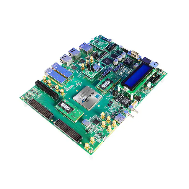
Board Overview
This section provides an overview of the Arria 10 SoC development board, including an annotated board
image and component descriptions. The figure below shows an overview of the board features.
© 2016 Altera Corporation. All rights reserved. ALTERA, ARRIA, CYCLONE, ENPIRION, MAX, MEGACORE, NIOS, QUARTUS and STRATIX words and logos are
trademarks of Altera Corporation and registered in the U.S. Patent and Trademark Office and in other countries. All other words and logos identified as
trademarks or service marks are the property of their respective holders as described at www.altera.com/common/legal.html. Altera warrants performance
of its semiconductor products to current specifications in accordance with Altera's standard warranty, but reserves the right to make changes to any
products and services at any time without notice. Altera assumes no responsibility or liability arising out of the application or use of any information,
product, or service described herein except as expressly agreed to in writing by Altera. Altera customers are advised to obtain the latest version of device
specifications before relying on any published information and before placing orders for products or services.
www.altera.com
101 Innovation Drive, San Jose, CA 95134
ISO
9001:2008
Registered
�5-2
UG-20004
2016.03.01
Board Overview
Figure 5-1: Overview of the Arria 10 SoC Development Board
FPGA_PB[0-3]
SMA EXT Refclk
PCI Express x8
SMA Ports
HPS EXT Refclk
FPGA
Ethernet
SFP + Optical Ports
HPS
Memory
Boot Memory
Daughtercard
HPS
Ethernet
SW1
Storage Memory
Daughtercard
Warm/Cold
Reset
USB
USB UART
HPS Clock Source Selection Jumper
SW3 JTAG Switch
Trace x16
FPGA HPS_DP[0-3]
USB Blaster II
FMC B Daughtercard
Port
JTAG Header
MAX V CPLD
System Controller
SW4
HPS_PB[0-3]
RS232 UART
FMC A Daughtercard
Port
FPGA_LED[0-3]
HPS_LED[0-3]
12V AC
Adapter
J42 FMCA
Voltage
J33 Clock Cleaner
Source Select
Clock Cleaner
Display Port
SDI Video
J32 FMCB
Voltage
FPGA
Memory
Linear
Dongle
Header
Trace x 4
Character LCD
Display
J30 FPGA
Power
On/Off
Switch
J58 FPGA
Power Jumper
Table 5-1: Board Components
Board Reference
Type
Description
Featured Devices
U23
FPGA
Arria 10 SoC, 10AS066N3F40E2SGE2, 1517-pin FBGA
U16
CPLD
MAX V CPLD System Controller, 5M2210ZF256, 256-pin
FBGA
U21
CPLD
IO_MUX_CPLD, 5M2210F256, 256-pin FBGA
Configuration, Status, and Setup Elements
J24
JTAG chain header
Provides access to the JTAG chain and disables the on-board
USB-Blaster II when using an external USB-Blaster cable.
SW3
JTAG chain control
DIP switch
Remove or include devices in the active JTAG chain.
Altera Corporation
Board Components
Send Feedback
�UG-20004
2016.03.01
Board Overview
Board Reference
Type
5-3
Description
SW4
MSEL DIP Switch
Controls the configuration scheme on the board. MSEL pin 0, 1
and 2 connect to the DIP switch.
J22
Mini-USB header
USB interface for FPGA programming and debugging through
the on-board USB-Blaster II JTAG via a type-B USB cable.
SW1
Function Dip switch Selects I2C Master, Controls PCIE slot power, and selects FGPA
image source.
S8
Program select push
button
Toggles the program select LEDs, which selects the program
image that loads from flash memory to the FPGA.
S7
Configure push
button
Load image from flash memory to the FPGA based on the
settings of the program select LEDs.
D18
Configuration done
LED
Illuminates when the FPGA is configured.
D19
Load LED
Illuminates when the MAX V CPLD 5M2210 System
Controller is actively configuring the FPGA.
D17
Error LED
Illuminates when the FPGA configuration from flash memory
fails.
D42
Power LED
Illuminates when 3.3-V power is present.
D13, D14
JTAG TX/RX LEDs
Indicates the transmit or receive activity of the JTAG chain.
The TX and RX LEDs flicker if the link is in use and active. The
LEDs are either off when not in use or on when in use but idle.
D20-D22
Program select LEDs Illuminates to show which flash memory image loads to the
FPGA when you press the program select push button.
D23, D24
FMC port present
LEDs
Illuminates when a daughtercard is plugged into the FMC port.
D11, D12
UART LEDs
Illuminates when UART transmitter and receiver are in use.
U42
Multi-output
oscillator
Si5338A quad-output fixed oscillator with 156.25 MHz,
100MHz, 25MHz, and 100MHz outputs.
U54
148.5-MHz
Oscillator
Programmable oscillator with a default frequency of 148.5
MHz. The frequency is programmable using the clock control
GUI running on the MAX V CPLD 5M2210 System Controller.
U51
50-MHz oscillator
50.000-MHz crystal oscillator for general purpose logic
U11
Multi-output
oscillator
Two 100 MHz outputs for PCIe application
J13, J14
Clock input SMA
connector
External clock inputs for the transceiver test port
J15
HPS SMA clock
Drives LVCMOS to HPS clock multiplexer.
U50
Multi-output
oscillator
Si5338A quad-output fixed oscillator with 125MHz, 270MHz,
100MHz, and 100MHz outputs.
Clock Circuitry
Board Components
Send Feedback
Altera Corporation
�5-4
UG-20004
2016.03.01
Board Overview
Board Reference
Type
Description
U49
Multi-output
oscillator
Si5338A quad-output fixed oscillator with four 133.33MHz
outputs.
U26
Multi-output clock
cleaner
LMK04828 Clock cleaner
General User Input/Output
D25-D32
User LEDs
Four user LEDs and four HPS LEDs. Illuminate when driven
low.
SW2
User DIP switch
User DIP switch. When the switch is ON, a logic 0 is selected.
S10
FGPA reset push
button
Reset the FPGA logic
S9
HPS External
Interrupt Push
button
HPS external interrupt
S3-S6
General user push
buttons
Four user push buttons and four HPS push buttons. Driven low
when pressed.
HPS reset push
buttons
HPS cold/warm reset push buttons
S11-S14
S1, S2
Memory Connectors
J26
HPS HILO Memory
connector
HPS memory card include DDR3 HILO memory card and
DDR4 HILO memory card
J23
Boot Flash
Connector
Boot flash card options include QSPI flash card, SD micro flash
card and NAND flash card
J27
FPGA HILO
Connector
FPGA memory card options include DDR3 HILO memory
card , and DDR4 HILO memory card
U19
FPCQ Flash
EPCQ flash for FPGA AS configuration
U45
I2C EEPROM
32-Kb I2C serial EEPROM
Communication Ports
J57
PCI Express socket
GEN3 x8 Socket
J29, J19
FMC port
J29 is a V57.1 compatible FMC connector. J19 is a FMC
connector defined by Altera 16 transceivers specification
J7, J8
SFP+ port
Two SFP+ ports
U12, J5
Gigabit Ethernet
port
RJ-45 connectors that provide HPS 10/100/1000 Ethernet
connections via a Micrel KSZ9031RN PHY.
U8, U9, J2, J3
Dual Gigabit
Ethernet port
Provide two SGMII Gigabit Ethernet ports through FPGA
transceivers
J10, U13
USB-UART Port
USB connector with USB-to-UART bridge for serial UART
interface.
J25
DB9 UART port,
DB9 RS-232 UART Port
Altera Corporation
Board Components
Send Feedback
�UG-20004
2016.03.01
Featured Device: Arria 10 SoC
Board Reference
Type
5-5
Description
J4, U22
USB OTG port
USB 2.0 On-The-Go (OTG) interface.
U5
Real-time clock
DS1339 device with built-in power sense circuit that detects
power failures and automatically switches to backup battery
supply, maintaining time keeping even when the board is not
powered.
J43
HPS Trace
connector
4-bit Trace for HPS debug
J20
FPGA Trace
FPGA 16-bit Trace
Video and Display Ports
J35
Character LCD
Connector that interfaces to the included 16 character × 2 line
LCD module along with two standoffs.
J36
Display port
connector
Display port interface
J48,J49, U29,U30 SDI Video port
HDBNC 75-Ohm SDI video interface
Power Supply
J36
DC input jack
Accepts 12-V DC power supply
SW5
Power switch
Switch to power on or off the board when power is supplied
from the DC input jack.
Featured Device: Arria 10 SoC
The Arria 10 SoC development board features an Arria 10 SoC 10AS066N3F40E2SGE2 device (U23) that
includes a hard processor system (HPS) with integrated ARM® Cortex™- A9 MPCore processor.
Table 5-2: Arria 10 SoC Features
Resources
10AS066N2F40
LE (K)
660
ALM
250, 540
Register
1,002,160
Memory (Kb)
42,660
18-bit x 18-bit Multiplier
3,356
Transceivers
48
Board Components
Send Feedback
Altera Corporation
�5-6
UG-20004
2016.03.01
MAX V CPLD 5M2210 System Controller
MAX V CPLD 5M2210 System Controller
The board utilizes the 5M2210ZF256 System Controller, an Altera MAX V CPLD, for the following
purposes:
•
•
•
•
•
•
•
•
Power sequencer
System reset controller
PCIe, FMC slot power sequencer
FPGA PS configuration controller
I2C Master controller
UART Level shifter
HPS SPI I/O expander
HPS Shared I/O
Table 5-3: MAX V CPLD System Controller Device Pin Out
I/O Bank
Board
Reference
Pin Name
Pin Type
I/O
Standar
d
Description
3
E14
P0V9Pgood
Schmitt trigger 3.3 V
input
Power good signal of 0.9
V power rail (Active high)
3
C14
HPS_Pgood
Schmitt trigger 3.3 V
input
HPS core voltage power
good signal
3
C15
PN0V95pgood
Schmitt trigger 3.3 V
input
0.95 V Power supply
power good signal (Active
high)
3
E13
1V0_Pgood
Schmitt trigger 3.3 V
input
1V0 Power supply power
good signal (Active high)
3
E12
1V8_Pgood
Schmitt trigger 3.3 V
input
1V8 Power supply power
good signal (Active high)
3
D15
2V5_Pgood
Schmitt trigger 3.3 V
input
2V5 Power supply power
good signal (Active high)
3
F14
3V3_Pgood
Schmitt trigger 3.3 V
input
3V3 Power supply power
good signal (Active high)
3
D16
PGM_LED2
OC
FPGA status LED.
3
F13
5V0_Pgood
Schmitt trigger 3.3 V
input
5V0 Power supply power
good signal (Active high)
3
E15
HILOHPS_VDDPGood
Schmitt trigger 3.3 V
input
HPS_HILO Power supply
power good signal
3
E16
HILO_VDDPGood
Schmitt trigger 3.3 V
input
HILO VDD power supply
power good signal
3
F15
HILO_VDDQPGood
Schmitt trigger 3.3 V
input
HILO VDDQ power
supply power good signal
3
G14
FMCAVADJPGood
Schmitt trigger 3.3 V
input
FMC VADJ Power supply
power good signal
Altera Corporation
3.3 V
Board Components
Send Feedback
�UG-20004
2016.03.01
MAX V CPLD 5M2210 System Controller
I/O Bank
Board
Reference
Pin Name
Pin Type
I/O
Standar
d
5-7
Description
3
F16
FMCBVADJPGood
Schmitt trigger 3.3 V
input
FMC VADJ Power supply
power good signal
3
G13
10V_Fail_n
Schmitt trigger 3.3 V
input
A10_12V input below
10.11 V (Active low)
3
G15
10V_good
Schmitt trigger 3.3 V
input
A10_12V input above
10.62 V (Active low)
3
G12
LTFAUL0
Input/Output
3.3 V
LT2977 Fault signal
3
G16
LTPWRGD
Input/Output
3.3 V
LT2977 Power good input
3
H14
FAC2MPgood
Output
3.3 V
30 ms delay after FMCA_
EN and FMCA_AUXEN
is enabled.
3
H15
FBC2MPgood
Output
3.3 V
30 ms delay after FMCB_
EN and FMCB_AUXEN
is enabled.
3
H13
FAM2CPgood
Schmitt trigger 3.3 V
input
This flag indicates the
power from FMC DC
card is good when MAX
V I/O CPLD BANK3
power uses FMC
POWER.
3
H16
TSENSE_ALERTn
Schmitt trigger 3.3 V
input
SMBUS Alert Bit when
I2C hangs
3
J13
OVERTEMPn
Schmitt trigger 3.3 V
input
Temperature is above
threshold
3
J16
FAN_EN
Output
3.3 V
FAN Enable (Active high)
3
J12
MAXV_USB_CLK
Clock input
3.3 V
Clock input from USBblaster
3
H12
NC
-
-
3
J14
NC
-
-
3
J15
A10_EN
Output
3.3 V
Arria 10 12 V input
enable (Active high)
3
K16
A10_0V9_EN
Output
3.3 V
0.9 V Power supply
enable (Active high)
3
K13
A10_0V95_EN
Output
3.3 V
0.95 V Power supply
enable (Active high)
3
K15
A10_1V0_EN
Output
3.3 V
1.0 V Power supply
enable (Active high)
3
K14
A10_1V8_EN
Output
3.3 V
1.8 V Power supply
enable (Active high)
Board Components
Send Feedback
Altera Corporation
�5-8
UG-20004
2016.03.01
MAX V CPLD 5M2210 System Controller
I/O Bank
Board
Reference
Pin Name
Pin Type
I/O
Standar
d
Description
3
L16
IO_EN
Output
3.3 V
Arria 10 I/O power enable
(Active high)
3
L11
PCIE_Auxen
Output
3.3 V
PCIE Aux power enable
(Active high)
3
L15
PCIE_EN
Output
3.3 V
PCIE 3V3 enable (Active
high)
3
L12
FMCA_AUXEN
Output
3.3 V
FMCA Aux power enable
(Active high)
3
M16
FMCA_EN
Output
3.3 V
FMCA3V3 enable (Active
high)
3
L13
FMCB_AUXEN
Output
3.3 V
FMCB Aux Power enable
(Active high)
3
M15
FMCB_EN
Output
3.3 V
FMCB3V3 enable (Active
high)
3
L14
Pmbus_Altertn
Schmitt trigger 3.3 V
input
Pmbus Alert Bit input
when I2C hangs.
3
N16
IO3V3_Discharge
Output
3.3 V
6A discharge load for
IO3V3 (Active high)
3
M13
PLL1V8_discharge
Output
3.3 V
3A discharge load for
IO3V3 (Active high)
3
N15
NC
3
N14
LTCNTRL0
Output
3.3 V
LT2977 Control 0
3
P15
LTCNTRL1
Output
3.3 V
LT2977 Control 1
3
P14
LTWDI_RESETN
Output
3.3 V
LT2977 reset
3
D13
FAPRSNT_n
Schmitt trigger 3.3 V
input
Detects signal of FMCA
DC card
3
D14
FBPRSNT_N
Schmitt trigger 3.3 V
input
Detects signal of FMCB
DC card
3
F11
USB_Vflagn
Schmitt trigger 3.3 V
input
Overcurrent flag of EXT
USB power
3
F12
NC
-
-
3
K12
NC
-
-
3
M14
NC
-
-
3
N13
NC
-
-
4
R1
A10_2L_SDA
Input/OC
3.3 V
I2C data line.
4
P4
A10_2L_SCL
OC
3.3 V
I2C clock line.
Altera Corporation
Board Components
Send Feedback
�UG-20004
2016.03.01
MAX V CPLD 5M2210 System Controller
I/O Bank
Board
Reference
Pin Name
Pin Type
I/O
Standar
d
5-9
Description
4
T2
A10I2CEN
Output
3.3 V
Enable Arria 10 HPS I2C.
(Active high)
4
P5
A10PMBUSEN
Output
3.3 V
Enable Arria 10 FPGA
I2C. (Active high)
4
R3
A10_PMBUSDIS_N
Output
3.3 V
Disables Arria 10 FPGA
PMBus access. (Active
low)
4
N5
UARTA_RX
Input
3.3 V
HPS UART RX input
from USB-UART.
4
P6
UARTA_TX
Output
3.3 V
HPS UART TX output to
USB-UART.
4
N6
PCIE_PRSNT2n
Input
3.3 V
Detects signal from PCIe
DC card.
4
R5
SFPA_LOS
Input
3.3 V
SFP+ A socket loss signal.
(Active low)
4
M6
SFPA_TXFAULT
Input
3.3 V
SFP+ A socket TX fault
signal. (Active low)
4
T5
SFPGA_TXDISABLE
Output
3.3 V
SFP+ A socket TX disable
signal. (Active low)
4
P7
SFPA_RATESEL0
Output
3.3 V
SFP+ A RX signaling rate
selection, 0
4.25 GBd
4
R6
SFPA_RATESEL1
Output
3.3 V
SFP +A TX signaling rate
selection, 0
4.25 GBd
4
N7
SFPB_TXDISABLE
Output
3.3 V
SFP+ B socket TX disable
signal. Active low
4
M7
SFPB_RATESEL0
Output
3.3 V
SFP+ B RX signaling rate
selection, 0
4.25 GBd
4
R7
SFPB_RATESEL1
Output
3.3 V
SFP +B TX signaling rate
selection, 0
4.25 GBd
4
P8
SFPB_LOS
Input
3.3 V
SFP+ A socket loss signal
(Active low)
4
T7
SFPB_TXFAULT
Input
3.3 V
SFP+ A socket tx fault
signal (Active low)
4
N8
SFPA_MOD0_PRSNTn
Input
3.3 V
Detect signal of SFP+
module in slot A (Active
low)
Board Components
Send Feedback
Altera Corporation
�5-10
UG-20004
2016.03.01
MAX V CPLD 5M2210 System Controller
I/O Bank
Board
Reference
Pin Name
Pin Type
I/O
Standar
d
Description
4
R8
SFPB_MOD0_PRSNTn
Input
3.3 V
Detect signal of SFP+
module in Slot B. (Active
low)
4
T8
NC
-
3.3 V
-
4
T9
NC
-
3.3 V
-
4
R9
Eneta_HPS_Intn
Input
3.3 V
Interrupt input from
Ethernet port 3
4
M9
Logic_resetn
Input
3.3 V
FPGA_logic reset input
4
M8
EXT_intn
Input
3.3 V
HPS External interrupt
4
M10
UART1_RX
Input
3.3 V
DB9 RS232 UART RX
4
R10
UART1_TX
Output
3.3 V
DB9 RS232 UART TX
4
N10
NC
Output
3.3 V
-
4
T11
LMK_reset
Output
3.3 V
LMK Clock cleaner reset
(Active high)
4
P10
NC
-
3.3 V
-
4
R11
NC
-
3.3 V
-
4
T12
ENET_HPS_RESETn
Output
3.3 V
Ethernet port 3 reset
(Active low)
4
N11
USB_RESET
Output
3.3 V
USB PHY reset (Active
high)
4
T13
PCIE_PERSTn
Output
3.3 V
This signal needs to be
held low if PCIE_auxEn
and PCIE_EN are not
active. 15 ms delay to set
this high after PCIE_EN is
active. PCIe RC slot reset,
active low.
4
R13
RESET_HPS_UARTA_N
Output
3.3 V
UART_RESET (Active
low)
4
R12
MAX2toMAXV0
Input/Output
3.3 V
Interbus between MAX II
and MAX V
4
P11
MAX2toMAXV1
Input/Output
3.3 V
Interbus between MAX II
and MAX V
4
N12
MAX2toMAXV2
Input/Output
3.3 V
Interbus between MAX II
and MAX V
4
R14
MAX2toMAXV3
Input/Output
3.3 V
Interbus between MAX II
and MAX V
4
P12
MAX2toMAXV4
Input/Output
3.3 V
Interbusbetween MAX II
and MAX V
Altera Corporation
Board Components
Send Feedback
�UG-20004
2016.03.01
MAX V CPLD 5M2210 System Controller
I/O Bank
Board
Reference
Pin Name
Pin Type
I/O
Standar
d
5-11
Description
4
T15
MAX2toMAXV5
Input/Output
3.3 V
Interbus between MAX II
and MAX V
4
R16
MAX2toMAXV6
Input/Output
3.3 V
Interbus between MAX II
and MAX V
4
P13
MAX2toMAXV7
Input/Output
3.3 V
Interbus between MAX II
and MAX V
4
M11
MAX2toMAXV8
Input/Output
3.3 V
Interbus between MAX II
and MAX V
4
M12
MAX2toMAXV9
Input/Output
3.3 V
Interbus between MAX II
and MAX V
4
N9
MAX2toMAXV10
Input/Output
3.3 V
Interbus between MAX II
and MAX V
4
R4
MAX2toMAXV11
Input/Output
3.3 V
Interbus between MAX II
and MAX V
4
T10
MAX2toMAXV12
Input/Output
3.3 V
Interbus between MAX II
and MAX V
4
T4
MAX2toMAXV13
Input/Output
3.3 V
Interbus between MAX II
and MAX V
2
D4
USER_LED_FPGA0
OC
2.5 V
USER FPGA LED 0
output
2
B1
USER_LED_FPGA1
OC
2.5 V
USER FPGA LED 1
output
2
C5
USER_LED_FPGA2
OC
2.5 V
USER FPGA LED 2
output
2
C4
USER_LED_FPGA3
OC
2.5 V
USER FPGA LED 3
output
2
B4
USER_LED_HPS0
OC
2.5 V
HPS LED 0 output
2
D6
USER_LED_HPS1
OC
2.5 V
HPS LED 1 output
2
E6
USER_LED_HPS2
OC
2.5 V
HPS LED 2 output
2
B5
USER_LED_HPS3
OC
2.5 V
HPS LED 3 output
2
A5
MAX_ERROR
OC
2.5 V
Board abnormal indicator
2
D7
MAX_LOAD
OC
2.5 V
FPGA status LED
2
B6
MAX_CONF_DONE
OC
2.5 V
FPGA status LED
2
E7
File_Presentn
Input
2.5 V
File flash present flag
2
C8
FACTORY_LOAD
OC
2.5 V
FPGA status LED
2
B7
PGM_LED0
OC
2.5 V
FPGA status LED
2
D8
PGM_SEL
Input
2.5 V
FPGA external trigger
Board Components
Send Feedback
Altera Corporation
�5-12
UG-20004
2016.03.01
MAX V CPLD 5M2210 System Controller
I/O Bank
Board
Reference
Pin Name
Pin Type
I/O
Standar
d
Description
2
A7
BF_Presentn
Input
2.5 V
Boot Flash present flag
2
B8
USER_DIPSW_HPS0
Input
2.5 V
User DIP HPS 0
2
A8
USER_DIPSW_HPS1
Input
2.5 V
User DIP HPS 1
2
A9
USER_DIPSW_HPS2
Input
2.5 V
User DIP HPS 2
2
E9
USER_DIPSW_HPS3
Input
2.5 V
User DIP HPS 3
2
B9
USER_DIPSW_FPGA0
Input
2.5 V
User DIP FPGA 0
2
D9
USER_DIPSW_FPGA1
Input
2.5 V
User DIP FPGA 1
2
A10
USER_DIPSW_FPGA2
Input
2.5 V
User DIP FPGA 2
2
C9
USER_DIPSW_FPGA3
Input
2.5 V
User DIP FPGA 3
2
E10
HPS_WARM_RESET1N
Input
2.5 V
Trace reset from MAX II
(Active low)
2
A11
HPS_WAM_RESETn
Input
2.5 V
Warm reset Pushbutton
(Active low)
2
B11
HPS_cold_resetn
Input
2.5 V
COLD reset Pushbuttion
(Active low)
2
A12
DC_Power_CTRL
Input
2.5 V
DC card power on/off
switch.
0 turn off DC power
1 turn on DC power
2
E11
I2C_flag
Input
2.5 V
I2C master selection, '0'
MAX V, '1' HPS
2
B12
PGM_CONFIG
Input
2.5 V
FGPA external trigger
2
C11
Security_mode
Input
2.5 V
FPGA mode bit
2
B13
PGM_LED1
OC
2.5 V
FPGA status LED
2
D12
MAXVtoMAXV4
Input/Output
2.5 V
Interbus between MAX
Vs
2
B14
MAXVtoMAXV5
Input/Output
2.5 V
Interbus between MAX
Vs
2
C13
MAXVtoMAXV6
Input/Output
2.5 V
Interbus between MAX
Vs
2
B16
MAXVtoMAXV7
Input/Output
2.5 V
Interbus between MAX
Vs
2
A13
MAXVtoMAXV8
Input/Output
2.5 V
Interbus between MAX
Vs
2
A15
MAXVtoMAXV9
Input/Output
2.5 V
Interbus between MAX
Vs
Altera Corporation
Board Components
Send Feedback
�UG-20004
2016.03.01
MAX V CPLD 5M2210 System Controller
I/O Bank
Board
Reference
Pin Name
Pin Type
I/O
Standar
d
5-13
Description
2
A2
USER_PB_HPS0
Input
2.5 V
HPS user push button 0
2
A4
USER_PB_HPS1
Input
2.5 V
HPS user push button 1
2
A6
USER_PB_HPS2
Input
2.5 V
HPS user push button 2
2
B10
USER_PB_HPS3
Input
2.5 V
HPS user push button 3
2
B3
USER_PB_FGPA0
Input
2.5 V
FPGA user push button 0
2
C10
USER_PB_FGPA1
Input
2.5 V
FPGA user push button 1
2
C12
USER_PB_FGPA2
Input
2.5 V
FPGA user push button 2
2
C6
USER_PB_FGPA3
Input
2.5 V
FPGA user push button 3
2
C7
MAXVtoMAXV3
Input/Output
2.5 V
Interbus between MAX
Vs
2
D10
MAXVtoMAXV10
Input/Output
2.5 V
Interbus between MAX
Vs
2
D11
MAXVtoMAXV11
Input/Output
2.5 V
Interbus between MAX
Vs
2
D5
MAXVtoMAXV12
Input/Output
2.5 V
Interbus between MAX
Vs
2
E8
MAXVtoMAXV13
Input/Output
2.5 V
Interbus between MAX
Vs
1
D3
MSEL0
Input
1.8 V
FPGA program mode
selection
1
C2
MSEL1
Input
1.8 V
FPGA program mode
selection
1
C3
MSEL2
Input
1.8 V
FPGA program mode
selection
1
E3
MFD0
Input/Output
1.8 V
EPCQ data0
1
D2
MFD1
Input/Output
1.8 V
EPCQ data1
1
E4
MFD2
Input/Output
1.8 V
EPCQ data2
1
D1
MFD3
Input/Output
1.8 V
EPCQ data3
1
E5
CLK_50M_MAX
Output
1.8 V
50 MHz clock to FPGA
1
F3
MFCSN
Output
1.8 V
EPCQ chip select.
1
E1
MFCLK
Output
1.8 V
EPCQ chip clock.
1
F4
HPSUARTA_TX
Input
1.8 V
HPS UART TX.
1
F2
HPSUARTA_RX
Output
1.8 V
HPS UART RX.
1
F1
SPIM1_MOSI
Input
1.8 V
SPI data input.
1
F6
SPIM1_SS0_N
Input
1.8 V
SPI chip select 0
Board Components
Send Feedback
Altera Corporation
�5-14
UG-20004
2016.03.01
MAX V CPLD 5M2210 System Controller
I/O Bank
Board
Reference
Pin Name
Pin Type
I/O
Standar
d
Description
1
G2
SPIM1_SS1_N
Input
1.8 V
SPI chip select 1
1
G3
SPIM1_MISO
Output
1.8 V
SPI data output.
1
G1
MAXVtoMAXV0
Input/Output
1.8 V
Interbus between MAX
Vs
1
G4
MAXVtoMAXV1
Input/Output
1.8 V
Interbus between MAX
Vs
1
H2
MAXVtoMAXV2
Input/Output
1.8 V
Interbus between MAX
Vs
1
G5
MAX_IO_CLK
Output
1.8 V
50Mhz Clock Output to
IO MAXV CPLD
1
H3
A10SH_GPIO0
Input/Output
1.8 V
HPS GPIO 5
1
J1
A10SH_GPIO1
Input/Output
1.8 V
HPS GPIO 13
1
H4
A10SH_GPIO2
Input/Output
1.8 V
HPS GPIO 16
1
J2
A10SH_GPIO3
Input/Output
1.8 V
HPS GPIO 17
1
H5
CLK_50M_MAX
Input
1.8 V
MAX V 50 MHz
reference clock
1
J5
SPIM1_CLK
Input
1.8 V
SPIM1_CLK input
1
J4
PS_D0
Output
1.8 V
Passive configure D0
1
K1
Nconfig
Output
1.8 V
Passive configure Nconfig
output
1
J3
DCLK
Output
1.8 V
Program Clock
1
K2
CVP_configDone
Input
1.8 V
CVP configure done
input during configura‐
tion, UART_TX after
configuration
1
K5
NSTATUS
Input
1.8 V
Status bit during FPGA
configuration
1
L1
conf_done
Input
1.8 V
Configuration done
1
L2
DEV_CLRN
Output
1.8
FPGA reset bit
1
K3
CRCerror
Output
1.8 V
CRCerror during configu‐
ration, UART_RX after
configuration
1
M1
Dedicated_tx
Input
1.8 V
Dedicated UART TX
input
1
M2
Daticated_RX
Output
1.8 V
Dedicated UART RX
Output
1
L4
FPGA_IO5
Input
1.8 V
FPGA_IO5
Altera Corporation
Board Components
Send Feedback
�UG-20004
2016.03.01
FPGA Configuration
I/O Bank
Board
Reference
Pin Name
Pin Type
I/O
Standar
d
5-15
Description
1
L3
FPGA_IO4
Output
1.8 V
FPGA_IO4
1
N1
FPGA_IO3
Output
1.8 V
FPGA_IO3
1
M4
FPGA_IO2
Output
1.8 V
FPGA_IO2
1
N2
FPGA_IO1
Input/Output
1.8 V
FPGA_IO1
1
M3
FPGA_IO0
Input/Output
1.8 V
FPGA_IO0
1
N3
PCIE1V8_PERSTn
Output
1.8 V
15 ms delay PCIE-PHY
0_Reset after PCIE_En is
activated if I/O MAX V
function is disabled.
1
P2
PCIE1V8_PERST1n
Output
1.8 V
PCIE_PHY1 reset must
be connected to the I/O
MAX V bit R16
(FBLAP33) via interbus if
the I/O MAX V function
is disabled.
1
E2
BQSPI_RESETN
Input/Output
1.8 V
Boot flash reset
1
F5
HPS_NPOR
Output
1.8 V
NPOR output of HPS
1
H1
HPS_NRST
Output
1.8 V
NRST output of HPS
1
K4
FILE_RESETN
Output
1.8 V
File flash reset
1
L5
Dedicated_OE
Input
1.8 V
Dedicated UART Enable
input
1
P3
M5_JTAG_TCK
Input
1.8 V
JTAG clock
1
L6
M5_JTAG_TDI
Input
1.8 V
JTAG data in
1
M5
M5_JTAG_TDO
Output
1.8 V
JTAG data out
1
N4
M5_JTAG_TMS
Input
1.8 V
JTAG_TMS
FPGA Configuration
This section describes the FPGA, I/O MUX CPLD, and MAX V CPLD 5M2210 System Controller device
programming methods supported by the Arria 10 SoC development board.
The Arria 10 SoC development board supports the following configuration methods using JTAG:
• On-board USB-Blaster II is the default method for configuring the FPGA using the Quartus Prime
Programmer in JTAG mode with the supplied USB cable.
• External Mictor connector for configuring the HPS using the ARM DS-5 Altera Edition software and
DSTREAM or JTAG debug and trace tools such as Lauterbach TRACE32.
• External USB-Blaster for configuring the FPGA when you connect the external USB-Blaster to the
JTAG header (J24).
Board Components
Send Feedback
Altera Corporation
�5-16
UG-20004
2016.03.01
System Controller Configuration
System Controller Configuration
J58 is used to turn off the FPGA power. The following table lists the status of each J58 configuration.
Table 5-4: J58 Jumper Settings
Board Reference
Description
J58
• OPEN: Normal application
• SHORT: No power to FPGA
Caution: The MAX V system controller controls the power sequence. The wrong configuration file may
damage the board.
The following procedure must be followed to program the system controller MAX V:
1. Short J58
2. Set SW3 Bits to:
Table 5-5: SW3 System Configuration Mode for System Controller MAX V Programming
Bit1
Bit2
Bit3
Bit4
Bit5
Bit6
Bit7
Bit8
ON
ON
ON
ON
ON
OFF
OFF
ON
Bit7
Bit8
3.
4.
5.
6.
7.
8.
9.
Turn on the power; the red LED will be flashing
Connect the USB cable to the on-board USB-Blaster II
Use “autodetect” in Quartus Prime to detect MAX V
Load the MAX V .pof file into Quartus Prime
Program the MAX V device
Turn off the power and remove J58
Set SW3 to normal operation mode
Refer to #iga1438035477237/table_hx1_jyz_zs for SW3 configuration.
10.Turn on the power; the red LED will always be on
FPGA Programming over On-Board USB-Blaster II
Table 5-6: SW3 Configuration for On-Board USB-Blaster II Mode
Bit1
OFF
Bit2
OFF
Bit3
ON
Bit4
ON
Bit5
ON
Bit6
OFF
OFF
OFF
This configuration method implements a mini-USB connector (J22), a USB 2.0 PHY device (U18), and an
Altera MAX II CPLD EPM1270M256C4N (U17) to allow FPGA configuration using a USB cable. This
USB cable connects directly between the USB connector on the board and a USB port on a PC running
the Quartus Prime software.
The on-board USB-Blaster II in the MAX II CPLD EPM1270M256C4N normally masters the JTAG
chain. The on-board USB-Blaster II shares the pins with the external header and is automatically disabled
when you connect an external USB-Blaster to the JTAG chain through the JTAG header (J24). In addition
to the JTAG interface, the on-board USB Blaster II has trace capabilities for HPS debug purposes. The
trace interface from the HPS routes to the on-board USB-Blaster II connection pins through the FPGA.
Altera Corporation
Board Components
Send Feedback
�UG-20004
2016.03.01
FPGA Programming over On-Board USB-Blaster II
5-17
Figure 5-2: JTAG Chain
TRST
TRST
TRST
FPGA Trace
HPS Trace
TCK
TMS
TDI
TDO
TCK
TMS
TDI
TDO
10-Pin
JTAG Header
TCK
TMS
TDI
TDO
Disable
TCK
TMS
TDI
TDO
Cypress On-Board
USB-Blaser II
MAX II JTAG Switch
TCK
TMS
TDI
TDO
TRST
A10 HPS/FPGA
TCK
TMS PCIE
TDI
TDO
TCK
TMS
TDI
TDO
FMC Port A
FMC Port B
TCK
TMS
TDI
TDO
IO_MUX
CPLD
TCK
TMS MAX V CPLD 5M2210
TDI System Controller
TDO
Flash
Memory
Note: If an external USB-Blaster (I/II) cable is plugged into the EXTERNAL JTAG HEADER, the MAX II
automatically uses it as the master despite any DIP switch setting.
The MAX II CPLD (EPM1270M256C4N) is dedicated to the on-board USB-Blaster II functionality only,
connecting to the USB 2.0 PHY device on one side and driving JTAG signals out the other side on the
GPIO pins. This device's own dedicated JTAG interface is routed to a small surface-mount header only
intended for debugging of first article prototypes.
Board Components
Send Feedback
Altera Corporation
�5-18
UG-20004
2016.03.01
FPGA Programming by HPS
FPGA Programming by HPS
The default method is to use the factory design—Golden Hardware Reference Design (GHRD).
Table 5-7: HPS FPGA Configuration
Configuration
Switch Position
SW4.4:OFF(Down)=MSEL2 is 0
HPS FPGA
SW4.3:OFF(Down)=MSEL1 is 0
SW4.2:OFF(Down)=MSEL0 is 0
Table 5-8: AS Configuration
Configuration
Switch Position
SW4.4:OFF(Down)=MSEL2 is 0
Active Serial (AS)
SW4.3:ON(Up)=MSEL1 is 1
SW4.2:ON(Up)=MSEL0 is 1
On power-up or by pressing the warm/cold reset push button, the HPS downloads the GHRD design
from boot flash to configure the FGPA. The D17 (Error LED) is turned off and D18 (Configuration done
LED) is turned on after the FPGA is configured.
By default the FPGA is configured by the HPS.
Refer to the GSRD User Manual for more information.
FPGA Programming by EPCQ Device
An EPCQ device is used for FPGA configuration in Active Serial (AS) mode on power up. The EPCQ
device with non-volatile memory features a simple six-pin interface and a small form factor. The EPCQ
supports AS x1 and x4 modes.
FPGA Programming over External USB-Blaster
The JTAG chain header provides another method for configuring the FPGA using an external USBBlaster device with the Quartus Prime Programmer running on a PC. To prevent contention between the
JTAG masters, the on-board USB-Blaster is automatically disabled when you connect an external USBBlaster to the JTAG chain through the JTAG chain header.
Altera Corporation
Board Components
Send Feedback
�UG-20004
2016.03.01
Status Elements
5-19
Status Elements
The development board includes status LEDs. This section describes the status elements.
Table 5-9: Board Specific LEDs
Board Reference
Type
Description
D18
Configuration done
LED
Illuminates when the FPGA is configured.
D19
Load LED
Illuminates when the MAX V CPLD 5M2210 System
Controller is actively configuring the FPGA.
D17
Error LED
Red LED illuminates when the FPGA configuration from flash
memory fails.
D42
Power LED
Illuminates when 3.3-V power is present.
D13, D14
JTAG TX/RX LEDs
Indicate the transmit or receive activity of the JTAG chain. The
TX and RX LEDs flicker if the link is in use and active. The
LEDs are either off when not in use or on when in use but idle.
D20-D22
Program select LEDs Illuminates to show which flash memory image loads to the
FPGA when you press the program select push button.
D23, D24
FMC port present
LEDs
Illuminates when a daughtercard is plugged into the FMC port.
D11, D12
UART LEDs
Illuminates when the UART transmitter and receiver are in use.
Setup Elements
The development board includes several different kinds of setup elements. This section describes the
following setup elements:
•
•
•
•
•
•
•
•
Board settings DIP switch
JTAG chain control DIP switch
FPGA configuration mode DIP switch
HPS jumpers
CPU reset push button
Logic reset push button
Program configuration push button
Program select push button
Board Settings DIP Switch
The board settings DIP switches (SW1 and SW4) control various features specific to the board and the
MAX V CPLD 5M2210 System Controller logic design. Refer to the "Defulat Switch and Jumper Settings"
section for more information on SW1 and SW4.
Related Information
Default Switch and Jumper Settings on page 3-2
Board Components
Send Feedback
Altera Corporation
�5-20
UG-20004
2016.03.01
JTAG Chain Control DIP Switch
JTAG Chain Control DIP Switch
The JTAG chain control DIP switch (SW3) either removes or includes devices in the active JTAG chain.
The SW3 switch select controls the JTAG master/slave select. The DIP switch MSTR switches control the
master select. The other 5 pins are bypass pins for the various available JTAG slaves. The following slaves
are available and can be bypassed by moving the corresponding bypass switch to the 'ON' position.
Table 5-10: JTAG Configuration Modes
Switch 3 Bit
Board Label
1
Arria 10
Function
ON- Arria10 JTAG Bypass
OFF- Arria10 JTAG Enable
2
I/O MAX V
ON- MAXV JTAG Bypass
OFF- MAXV JTAG Enable
3
FMCA
ON- FMCA JTAG Bypass
OFF- FMCA JTAG Enable
4
FMCB
ON- FMCB JTAG Bypass
OFF- FMCB JTAG Enable
5
PCIe
ON- PCIe JTAG Bypass
OFF- PCIe JTAG Enable
6
MSTR[0]
Refer to Table 5-11
7
MSTR[1]
Refer to Table 5-11
8
MSTR[2]
Refer to Table 5-11
The MSTR switch settings and their meanings can be seen in the table below.
Table 5-11: Modes for Master Switches
MSTR2
MSTR1
MSTR0
Modes
ON
ON
ON
BOOT
OFF
ON
ON
FMCA JTAG Master
ON
OFF
ON
FMCB JTAG Master
ON
ON
OFF
FTRACE JTAG Master
OFF
OFF
OFF
On-Board USB-Blaster II JTAG
Master
ON
OFF
OFF
System Configuration Mode
OFF
ON
OFF
GUI Test Mode
OFF
OFF
ON
Reserved
Altera Corporation
Board Components
Send Feedback
�UG-20004
2016.03.01
JTAG Chain Control DIP Switch
5-21
The bypass switch settings dictate which slaves are in/out of the chain, but see below for the order if all
were enabled in the chain.
1.
2.
3.
4.
5.
Arria 10
IO_MAXV
PCIe
FMCA
FMCB
Board Components
Send Feedback
Altera Corporation
�5-22
UG-20004
2016.03.01
Reference Clock Source Selection
Reference Clock Source Selection
The HPS jumpers define the bootstrap options for the HPS—boot source, mode, HPS clocks settings,
power-on-reset (POR) mode and peripherals selection.
Table 5-12: HPS Jumpers
Board Reference
J17, J16
Schematic Signal Name
OSC2_CLK_SEL [1:0]
Description
Selects the source of OSC2 clock:
00—Select 25 MHz clock source
01—Select external source via SMA
connector
10—Select 33 MHz on-board oscillator
J30
HPS voltage selection
Short—HPS core voltage is 0.95V
Open—HPS core voltage is 0.9V
CPU Reset Push Button
Table 5-13: CPU Reset Push Buttons
Push Button
Description
S1
HPS_WARM_RESET push button.
S2
HPS_COLD_RESET push button.
The HPS_NRST input is driven by HPS_WARM_RESET. The HPS_NPOR input is driven by HPS_COLD_RESET.
Logic Reset Push Button
The logic reset push button (S10) is an input to the MAX V CPLD 5M2210 System Controller. This push
button is the default reset for the CPLD logic and FPGA.
General User Input/Output
All user-defined push buttons, DIP switches and LEDs are connected to the MAX V System Controller.
The IO_MUX CPLD maps user-defined signals to FPGA I/Os as defined in the GHRD. The following
section describes the mapping table.
Character LCD
The development board includes a single 10-pin 0.1" pitch single-row header that interfaces to a 2 line ×
16 character Lumex character LCD using a standard I2C interface connected to the HPS.
For more information such as timing, character maps, interface guidelines, and other related documenta‐
tion, visit http://www.newhavendisplay.com.
Altera Corporation
Board Components
Send Feedback
�UG-20004
2016.03.01
Clock Circuitry
5-23
Clock Circuitry
This section describes the board's clock inputs and outputs.
On-Board Oscillators
Figure 5-3: FPGA I/O Bank Clock Connection
Match the colors in the above figure to match the FPGA I/O banks with its corresponding clock sources.
Board Components
Send Feedback
Altera Corporation
�5-24
UG-20004
2016.03.01
Components and Interfaces
Components and Interfaces
This section describes the development board's communication ports and interface cards relative to the
Arria 10 SoC device. The development board supports the following communication ports:
•
•
•
•
•
•
•
•
PCI Express Gen3 root complex and end point
10/100/1000 Ethernet (HPS)
10/100/1000 Ethernet (FPGA)
FMC
RS-232 UART (HPS)
Real-Time Clock
SFP+
I2C interface
PCI Express
The PCIe RC interface on the development board supports auto-negotiating channel width from x1 to x8
as well as the connection speed of Gen3 at 8 Gbps/lane.
The PCI express end point interface is connected to the FMCB slot. A special PCIE-FMC cable
(HDR-181157-01-PCIEC) made by SAMTEC must be plugged into the FMCB slot for the PCIe EP
application.
For the PCIe RC application, the PCIE_REFCLK_P/N signal is a 100-MHz differential input that is driven to
the daughtercard through the PCIe edge connector. This signal connects directly to a Arria 10 SoC
REFCLK input pin pair using DC coupling. The I/O standard is High-Speed Current Steering Logic
(HCSL).
Figure 5-4: PCI Express Reference Clock Levels
Vmax = 1.15 V
REFCLK VCROSS MAX = 550 mV
VCROSS MIN = 250 mV
REFCLK +
VMIN = -0.30 V
The PCI Express edge connector also has a presence detect feature for the motherboard to determine if a
card is installed.
Altera Corporation
Board Components
Send Feedback
�UG-20004
2016.03.01
PCI Express
5-25
Table 5-14: PCI Express FPGA Pin Assignments
Arria 10 SoC Pin Name
Schematic Signal Name
Direction
Description
Y38
PCIE_TX_N7
Output
PCIe RC Channel 7 Transmitter
Y39
PCIE_TX_P7
Output
PCIe RC Channel 7 Transmitter
Y34
PCIE_RX_N7
Input
PCIe RC Channel 7 Receiver
Y35
PCIE_RX_P7
Input
PCIe RC Channel 7 Receiver
AA36
PCIE_TX_N6
Output
PCIe RC Channel 6 Transmitter
AA37
PCIE_TX_P6
Output
PCIe RC Channel 6 Transmitter
AA32
PCIE_RX_N6
Input
PCIe RC Channel 6 Receiver
AA33
PCIE_RX_P6
Input
PCIe RC Channel 6 Receiver
AB38
PCIE_TX_N5
Output
PCIe RC Channel 5 Transmitter
AB39
PCIE_TX_P5
Output
PCIe RC Channel 5 Transmitter
AB34
PCIE_RX_N5
Input
PCIe RC Channel 5 Receiver
AB35
PCIE_RX_P5
Input
PCIe RC Channel 5 Receiver
AC36
PCIE_TX_N4
Output
PCIe RC Channel 4 Transmitter
AC37
PCIE_TX_P4
Output
PCIe RC Channel 4 Transmitter
AB30
PCIE_RX_N4
Input
PCIe RC Channel 4 Receiver
AB31
PCIE_RX_P4
Input
PCIe RC Channel 4 Receiver
AD38
PCIE_TX_N3
Output
PCIe RC Channel 3 Transmitter
AD39
PCIE_TX_P3
Output
PCIe RC Channel 3 Transmitter
AC32
PCIE_RX_N3
Input
PCIe RC Channel 3 Receiver
AC33
PCIE_RX_P3
Input
PCIe RC Channel 3 Receiver
AE36
PCIE_TX_N2
Output
PCIe RC Channel 2 Transmitter
AE37
PCIE_TX_P2
Output
PCIe RC Channel 2 Transmitter
AD34
PCIE_RX_N2
Input
PCIe RC Channel 2 Receiver
AD35
PCIE_RX_P2
Input
PCIe RC Channel 2 Receiver
AE28
-
Input
Pull down to Ground, no use
AE29
-
Input
Pull down to Ground, no use
Board Components
Send Feedback
Altera Corporation
�5-26
UG-20004
2016.03.01
10/100/1000 Ethernet (HPS)
10/100/1000 Ethernet (HPS)
The development board supports an RJ-45 10/100/1000 base-T Ethernet using an external Micrel
KSZ9031RN PHY and the HPS EMAC function. The PHY-to-MAC interface employs RGMII connection
using four data lines at 250 Mbps each for a connection speed of 1 Gbps.
The PHY interfaces to an RJ-45 model with internal magnetics that can be used for driving copper lines
with Ethernet traffic.
Figure 5-5: RGMII Interface between HPS (MAC) and PHY
RGMII
MAC
Single-Port RGMII
Micrel KSZ9031RN
RJ-45
Table 5-15: Ethernet (HPS) Pin Assignments
FPGA Pin Number
Shared I/O Bit
Schematic Signal Name
Description
H18
GPIO0_IO12
ENET_HPS_GTX_CLK
EMAC0 RGMII TX Clock
H19
GPIO0_IO13
ENET_HPS_TX_EN
EMAC0 RGMII enable
F18
GPIO0_IO14
ENET_HPS_RX_CLK
EMAC0 RGMII RX Clock
G17
GPIO0_IO15
ENET_HPS_RX_DV
EMAC0 RGMII RX DV flag
E20
GPIO0_IO16
ENET_HPS_TXD0
EMAC0 RGMII TXD0
F20
GPIO0_IO17
ENET_HPS_TXD1
EMAC0 RGMII TXD1
G20
GPIO0_IO18
ENET_HPS_RXD0
EMAC0 RGMII RXD0
G21
GPIO0_IO19
ENET_HPS_RXD1
EMAC0 RGMII RXD1
F19
GPIO0_IO20
ENET_HPS_TXD2
EMAC0 RGMII TXD2
G19
GPIO0_IO21
ENET_HPS_TXD3
EMAC0 RGMII TXD3
F22
GPIO0_IO22
ENET_HPS_RXD2
EMAC0 RGMII RXD2
G22
GPIO0_IO23
ENET_HPS_RXD3
EMAC0 RGMII RXD3
H23
GPIO1_IO8
ENETB_MDIO
EMAC2 MDIO
J23
GPIO1_IO9
ENETB_MDC
EMAC2 MDIO
K21
GPIO1_IO10
ENET_HPS_MDIO
EMAC2 MDIO
K20
GPIO1_IO11
ENET_HPS_MDC
EMAC2 MDIO
The Micrel KSZ9031RN PHY uses a multi-level POR bootstrap encoding scheme to allow a small set of
I/O pins (7) to set up a very large number of default settings within the device. The related I/O pins have
integrated pull-up or pull-down resistors to configure the device.
Altera Corporation
Board Components
Send Feedback
�UG-20004
2016.03.01
10/100/1000 Ethernet (HPS)
5-27
Table 5-16: Ethernet PHY (HPS) Bootstrap Encoding Scheme
Board Reference (U12)
Schematic Signal Name
Description
Strapping Option
17
ENET_HPS_LED1_LINK
PHY address bit 0
Pulled high
15
ENET_HPS_LED2_LINK
PHY address bit 1
Pulled high
32
ENET_HPS_RXD0
Mode 0
Pulled high
31
ENET_HPS_RXD1
Mode 1
Pulled high
28
ENET_HPS_RXD2
Mode 2
Pulled high
27
ENET_HPS_RXD3
Mode 3
Pulled high
35
ENET_HPS_RX_CLK
PHY address bit 2
Pulled high
33
ENET_HPS_RX_DV
Clock enable
Pulled low
41
CLK125_NDO_LED_MODE
Single LED mode
Pulled high
Board Components
Send Feedback
Altera Corporation
�5-28
UG-20004
2016.03.01
10/100/1000 Ethernet (FPGA)
10/100/1000 Ethernet (FPGA)
The development board supports two RJ45 10/100/1000 base-T Ethernet using Marvell 88E1111. SGMII
AC coupling interface is used between PHY and FGPA transceiver.
Figure 5-6: MII Interface between FPGA (MAC) and PHY
(1E,0)
MARVELL
88E1111 SGMII
PHY
RJ-45
FPGA SGMII
MAC
(1E,1)
MARVELL
88E1111 SGMII
PHY
RJ-45
Table 5-17: Ethernet (FPGA) Pin Assignments
FPGA Pin Assignment
Schematic Signal Name
Direction
Description
AK38
ENETA_TX_N
Output
Ethernet Port A Transmitter
AK39
ENETA_TX_P
Output
Ethernet Port A Transmitter
AG32
ENETA_RX_N
Input
Ethernet Port A Receiver
AG33
ENETA_RX_P
Input
Ethernet Port A Receiver
AL36
ENETB_TX_N
Output
Ethernet Port B Transmitter
AL37
ENETB_TX_P
Output
Ethernet Port B Transmitter
AH34
ENETB_RX_N
Input
Ethernet Port B Receiver
AH35
ENETB_RX_P
Input
Ethernet Port B Receiver
AG29
CLK_ENET_FPGA_P
Input
125MHz Reference clock from
Clock Synthesizer
AG28
CLK_ENET_FPGA_N
Input
125MHz Reference clock from
Clock Synthesizer
Altera Corporation
Board Components
Send Feedback
�UG-20004
2016.03.01
FMC
5-29
FMC
The FMCA slot is compliant with the V57.1 spec. All FMC V57.1 1.8V daughtercards can be plugged into
the FMCA slot. The FMCB slot is designed based on the Altera 16-transceiver FMCB specification.
Note: Check the signal connections if your FMC card must be put in the FMCB slot.
Table 5-18: FMC Port A Transceiver Pin Assignments
FPGA Pin Assignment
Schematic Signal Name
Direction
Description
E36
FAD9C2MN
Output
FMCA Slot Channel 9
transmitter
E37
FAD9C2MP
Output
FMCA Slot Channel 9
transmitter
K30
FAD9M2CN
Input
FMCA Slot Channel 9
receiver
K31
FAD9M2CP
Input
FMCA Slot Channel 9
receiver
F34
FAD8C2MN
Output
FMCA Slot Channel 8
transmitter
F35
FAD8C2MP
Output
FMCA Slot Channel 8
transmitter
K34
FAD8M2CN
Input
FMCA Slot Channel 8
receiver
K35
FAD8M2CP
Input
FMCA Slot Channel 8
receiver
F38
FAD7C2MN
Output
FMCA Slot Channel 7
transmitter
F39
FAD7C2MP
Output
FMCA Slot Channel 7
transmitter
L32
FAD7M2CN
Input
FMCA Slot Channel 7
receiver
L33
FAD7M2CP
Input
FMCA Slot Channel 7
receiver
G36
FAD6C2MN
Output
FMCA Slot Channel 6
transmitter
G37
FAD6C2MP
Output
FMCA Slot Channel 6
transmitter
M30
FAD6M2CN
Input
FMCA Slot Channel 6
receiver
M31
FAD6M2CP
Input
FMCA Slot Channel 6
receiver
L29
LMK_FMCCLK_P
input
FMCA reference clock
from Clock cleaner
Board Components
Send Feedback
Altera Corporation
�5-30
UG-20004
2016.03.01
FMC
FPGA Pin Assignment
Schematic Signal Name
Direction
Description
L28
LMK_FMCCLK_N
input
FMCA reference clock
from Clock cleaner
N29
FAGBTCLK0M2CP
input
FMCA SLOT reference
Clock 0
N28
FAGBTCLK0M2CN
input
FMCA SLOT reference
Clock 0
H38
FAD5C2MN
Output
FMCA Slot Channel 5
transmitter
H39
FAD5C2MP
Output
FMCA Slot Channel 5
transmitter
M34
FAD5M2CN
Input
FMCA Slot Channel 5
receiver
M35
FAD5M2CP
Input
FMCA Slot Channel 5
receiver
J36
FAD4C2MN
Output
FMCA Slot Channel 4
transmitter
J37
FAD4C2MP
Output
FMCA Slot Channel 4
transmitter
N32
FAD4M2CN
Input
FMCA Slot Channel 4
receiver
N33
FAD4M2CP
Input
FMCA Slot Channel 4
receiver
K38
FAD3C2MN
Output
FMCA Slot Channel 3
transmitter
K39
FAD3C2MP
Output
FMCA Slot Channel 3
transmitter
P30
FAD3M2CN
Input
FMCA Slot Channel 3
receiver
P31
FAD3M2CP
Input
FMCA Slot Channel 3
receiver
L36
FAD2C2MN
Output
FMCA Slot Channel 2
transmitter
L37
FAD2C2MP
Output
FMCA Slot Channel 2
transmitter
P34
FAD2M2CN
Input
FMCA Slot Channel 2
receiver
P35
FAD2M2CP
Input
FMCA Slot Channel 2
receiver
M38
FAD1C2MN
Output
FMCA Slot Channel 1
transmitter
Altera Corporation
Board Components
Send Feedback
�UG-20004
2016.03.01
FMC
FPGA Pin Assignment
Schematic Signal Name
Direction
5-31
Description
M39
FAD1C2MP
Output
FMCA Slot Channel 1
transmitter
R32
FAD1M2CN
Input
FMCA Slot Channel 1
receiver
R33
FAD1M2CP
Input
FMCA Slot Channel 1
receiver
N36
FAD0C2MN
Output
FMCA Slot Channel 0
transmitter
N37
FAD0C2MP
Output
FMCA Slot Channel 0
transmitter
T30
FAD0M2CN
Input
FMCA Slot Channel 0
receiver
T31
FAD0M2CP
Input
FMCA Slot Channel 0
receiver
R29
FAGBTCLK1M2CP
input
FMCA SLOT reference
Clock 1
R28
FAGBTCLK1M2CN
input
FMCA SLOT reference
Clock 1
Table 5-19: FMC Port B Transceiver Pin Assignments
FPGA Pin Assignment
Schematic Signal Name
Direction
Description
U29
REFCLK1_FMCB_P
input
FMCB Reference Clock
1 from Clock
synthesizer
U28
REFCLK1_FMCB_N
input
FMCB Reference Clock
1 from Clock
synthesizer
P38
FBD15C2MN
Output
FMCB Slot Channel 15
transmitter
P39
FBD15C2MP
Output
FMCB Slot Channel 15
transmitter
T34
FBD15M2CN
Input
FMCB Slot Channel 15
receiver
T35
FBD15M2CP
Input
FMCB Slot Channel 15
receiver
R36
FBD14C2MN
Output
FMCB Slot Channel 14
transmitter
R37
FBD14C2MP
Output
FMCB Slot Channel 14
transmitter
U32
FBD14M2CN
Input
FMCB Slot Channel 14
receiver
Board Components
Send Feedback
Altera Corporation
�5-32
UG-20004
2016.03.01
FMC
FPGA Pin Assignment
Schematic Signal Name
Direction
Description
U33
FBD14M2CP
Input
FMCB Slot Channel 14
receiver
T38
FBD13C2MN
Output
FMCB Slot Channel 13
transmitter
T39
FBD13C2MP
Output
FMCB Slot Channel 13
transmitter
V30
FBD13M2CN
Input
FMCB Slot Channel 13
receiver
V31
FBD13M2CP
Input
FMCB Slot Channel 13
receiver
U36
FBD12C2MN
Output
FMCB Slot Channel 12
transmitter
U37
FBD12C2MP
Output
FMCB Slot Channel 12
transmitter
V34
FBD12M2CN
Input
FMCB Slot Channel 12
receiver
V35
FBD12M2CP
Input
FMCB Slot Channel 12
receiver
V38
FBD11C2MN
Output
FMCB Slot Channel 11
transmitter
V39
FBD11C2MP
Output
FMCB Slot Channel 11
transmitter
W32
FBD11M2CN
Input
FMCB Slot Channel 11
receiver
W33
FBD11M2CP
Input
FMCB Slot Channel 11
receiver
W36
FBD10C2MN
Output
FMCB Slot Channel 10
transmitter
W37
FBD10C2MP
Output
FMCB Slot Channel 10
transmitter
Y30
FBD10M2CN
Input
FMCB Slot Channel 10
receiver
Y31
FBD10M2CP
Input
FMCB Slot Channel 10
receiver
W29
FBGBTCLK1M2CP
input
Reference Clock from
FMCB slot channel 1
W28
FBGBTCLK1M2CN
input
Reference Clock from
FMCB slot channel 1
AM38
FBD7C2MN
Output
FMCB Slot Channel 7
transmitter or PCIE EP
Channel 7 transmitter
Altera Corporation
Board Components
Send Feedback
�UG-20004
2016.03.01
FMC
FPGA Pin Assignment
Schematic Signal Name
Direction
5-33
Description
AM39
FBD7C2MP
Output
FMCB Slot Channel 7
transmitter or PCIE EP
Channel 7 transmitter
AH30
FBD7M2CN
Input
FMCB Slot Channel 7
receiver or PCIE EP
Channel 7 receiver
AH31
FBD7M2CP
Input
FMCB Slot Channel 7
receiver or PCIE EP
Channel 7 receiver
AN36
FBD6C2MN
Output
FMCB Slot Channel 6
transmitter or PCIE EP
Channel 6 transmitter
AN37
FBD6C2MP
Output
FMCB Slot Channel 6
transmitter or PCIE EP
Channel 6 transmitter
AJ32
FBD6M2CN
Input
FMCB Slot Channel 6
receiver or PCIE EP
Channel 6 receiver
AJ33
FBD6M2CP
Input
FMCB Slot Channel 6
receiver or PCIE EP
Channel 6 receiver
AP38
FBD5C2MN
Output
FMCB Slot Channel 5
transmitter or PCIE EP
Channel 5 transmitter
AP39
FBD5C2MP
Output
FMCB Slot Channel 5
transmitter or PCIE EP
Channel 5 transmitter
AK34
FBD5M2CN
Input
FMCB Slot Channel 5
receiver or PCIE EP
Channel 5 receiver
AK35
FBD5M2CP
Input
FMCB Slot Channel 5
receiver or PCIE EP
Channel 5 receiver
AP34
FBD4C2MN
Output
FMCB Slot Channel 4
transmitter or PCIE EP
Channel 4 transmitter
AP35
FBD4C2MP
Output
FMCB Slot Channel 4
transmitter or PCIE EP
Channel 4 transmitter
AK30
FBD4M2CN
Input
FMCB Slot Channel 4
receiver or PCIE EP
Channel 4 receiver
Board Components
Send Feedback
Altera Corporation
�5-34
UG-20004
2016.03.01
FMC
FPGA Pin Assignment
Schematic Signal Name
Direction
Description
AK31
FBD4M2CP
Input
FMCB Slot Channel 4
receiver or PCIE EP
Channel 4 receiver
AR36
FBD3C2MN
Output
FMCB Slot Channel 3
transmitter or PCIE EP
Channel 3 transmitter
AR37
FBD3C2MP
Output
FMCB Slot Channel 3
transmitter or PCIE EP
Channel 3 transmitter
AL32
FBD3M2CN
Input
FMCB Slot Channel 3
receiver or PCIE EP
Channel 3 receiver
AL33
FBD3M2CP
Input
FMCB Slot Channel 3
receiver or PCIE EP
Channel 3 receiver
AT38
FBD2C2MN
Output
FMCB Slot Channel 2
transmitter or PCIE EP
Channel 2 transmitter
AT39
FBD2C2MP
Output
FMCB Slot Channel 2
transmitter or PCIE EP
Channel 2 transmitter
AM34
FBD2M2CN
Input
FMCB Slot Channel 2
receiver or PCIE EP
Channel 2 receiver
AM35
FBD2M2CP
Input
FMCB Slot Channel 2
receiver or PCIE EP
Channel 2 receiver
AL29
REFCLK0_FMCB_P
Input
FMCB Reference Clock
0 from Clock
synthesizer
AL28
REFCLK0_FMCB_N
Input
FMCB Reference Clock
0 from Clock
synthesizer
AN29
FBGBTCLK0M2CP
Input
FMCB slot reference
clock channel 0 or
PCIE EP reference
clock
AN28
FBGBTCLK0M2CN
Input
FMCB slot reference
clock channel 0 or
PCIE EP reference
clock
AT34
FBD1C2MN
Output
FMCB Slot Channel 1
transmitter or PCIE EP
Channel 1 transmitter
Altera Corporation
Board Components
Send Feedback
�UG-20004
2016.03.01
FMC
FPGA Pin Assignment
Schematic Signal Name
Direction
5-35
Description
AT35
FBD1C2MP
Output
FMCB Slot Channel 1
transmitter or PCIE EP
Channel 1 transmitter
AM30
FBD1M2CN
Input
FMCB Slot Channel 1
receiver or PCIE EP
Channel 1 receiver
AM31
FBD1M2CP
Input
FMCB Slot Channel 1
receiver or PCIE EP
Channel 1 receiver
AU36
FBD0C2MN
Output
FMCB Slot Channel 0
transmitter or PCIE EP
Channel 0 transmitter
AU37
FBD0C2MP
Output
FMCB Slot Channel 0
transmitter or PCIE EP
Channel 0 transmitter
AN32
FBD0M2CN
Input
FMCB Slot Channel 0
receiver or PCIE EP
Channel 0 receiver
AN33
FBD0M2CP
Input
FMCB Slot Channel 0
receiver or PCIE EP
Channel 0 receiver
AV38
FBD9C2MN
Output
FMCB Slot Channel 9
transmitter
AV39
FBD9C2MP
Output
FMCB Slot Channel 9
transmitter
AP30
FBD9M2CN
Input
FMCB Slot Channel 9
receiver
AP31
FBD9M2CP
Input
FMCB Slot Channel 9
receiver
AV34
FBD8C2MN
Output
FMCB Slot Channel 8
transmitter
AV35
FBD8C2MP
Output
FMCB Slot Channel 8
transmitter
AR32
FBD8M2CN
Input
FMCB Slot Channel 8
receiver
AR33
FBD2M2CP
Input
FMCB Slot Channel 8
receiver
The FMCA slot is designed to be compatible with the requirements of FMC V57.1. This slot can be used
to support an external FMC memory card (DDR3 or DDR4).
Board Components
Send Feedback
Altera Corporation
�5-36
UG-20004
2016.03.01
FMC
Table 5-20: FMCA LVDS Signal I/O Assignment
BANK
Pin Number
Schematic Signal
Name
DDR3 Interface
(optional)
DDR4 Interface
(optional)
3H
P15
FAHAN0
DDR3 DQ4
DDR4 DQ4
3H
P14
FAHAP0
DDR3 DM0
DDR4 LDM_n0
3H
N14
FAHAN1
DDR3 DQ5
DDR4 DQ5
3H
M14
FAHAP1
DDR3 DQ6
DDR4 DQ6
3H
J14
FAHAN2
DDR3 DQ1
DDR4 DQ1
3H
J13
FAHAP2
DDR3 DQ0
DDR4 DQ0
3H
L15
FAHAN3
DDR3 DQS 0n
DDR4 DQSL_n0
3H
L14
FAHAP3
DDR3 DQS 0p
DDR4 DQSL_p0
3H
L13
FAHAN4
DDR3 DQ2
DDR4 DQ2
3H
L12
FAHAP4
DDR3 DQ3
DDR4 DQ3
3H
K13
FAHAN5
DDR3 DQ7
DDR4 DQ7
3H
K12
FAHAP5
3H
H14
FALAN0
DDR3 DQ9
DDR4 DQ9
3H
G14
FALAP0
DDR3 DQ8
DDR4 DQ8
3H
D14
FALAN3
DDR3 DQ11
DDR4 DQ11
3H
C14
FALAP3
DDR3 DQ10
DDR4 DQ10
3H
D13
FALAN2
DDR3 DQ14
DDR4 DQ14
3H
C13
FALAP2
DDR3 DQ12
DDR4 DQ12
3H
E13
FA_LA_DEVCLK_
N
DDR3 DQS1n
DDR4 DQSU0n
3H
E12
FA_LA_DEVCLK_P DDQ3 DQS1p
DDQ4 DQSU0p
3H
H13
FALAN4
DDR3 DQ13
DDQ4 DQ13
3H
H12
FALAP4
240-Ohm reference
resistor
240-Ohm
reference resistor
3H
F14
FA_LA_SYSREF_N
DDR3 DQ15
DDR4 DQ15
3H
F13
FA_LA_SYSREF_P
DDR3 DM1
DDR4 UDM_n0
3H
C12
FAHAN6
DDR3 DQ20
DDR4 DQ20
3H
C11
FAHAP6
DDR3 DQ22
DDR4 DQ22
3H
E11
FAHAN7
DDR3 DQ17
DDR4 DQ17
3H
D11
FAHAP7
DDR3 DQ18
DDR4 DQ18
3H
G12
FAHAN8
DDR3 DQ19
DDR4 DQ19
3H
F12
FAHAP8
DDR3 DQ16
DDR4 DQ16
Altera Corporation
Board Components
Send Feedback
�UG-20004
2016.03.01
FMC
BANK
Pin Number
Schematic Signal
Name
DDR3 Interface
(optional)
5-37
DDR4 Interface
(optional)
3H
G10
FAHAN9
DDR3 DQSn2
DDR4 DQSL1n
3H
F10
FAHAP9
DDR3 DQSp2
DDR4 DQSl1p
3H
E10
FAHAN10
DDR3 DM2
DDR4 LDM_n1
3H
D10
FAHAP10
DDR3 DQ21
DDR4 DQ21
3H
H11
FAHAN11
DDR3DQ23
DDR4DQ23
3H
G11
FAHAP11
3H
B10
FALAN6
DDR3 DMA3
DDR4 UDM_n1
3H
A10
FALAP6
DDR3 DQ31
DDR4 DQ31
3H
B9
FALAN7
DDR3 DQ30
DDR4 DQ30
3H
A9
FALAP7
3H
B12
FALAN8
DDR3 DQ29
DDR4 DQ29
3H
B11
FALAP8
DDR3 DQ28
DDR4 DQ28
3H
A13
FALAN9
DDR3 DQSn3
DDR4 DQSU1n
3H
A12
FALAP9
DDR3 DQSp3
DDR4 DQSU1p
3H
A8
FALAN10
DDR3 DQ25
DDR4 DQ25
3H
A7
FALAP10
DDR3 DQ26
DDR4 DQ26
3H
D9
FALAN11
DDR3 DQ24
DDR4 DQ24
3H
C9
FALAP11
DDR3 DQ27
DDR4 DQ27
3G
F8
FAHAN12
DQ of DDR3 Byte 8
DQ of DDR4
Byte 8
3G
E8
FAHAP12
DQ of DDR3 Byte 8
DQ of DDR4
Byte 8
3G
C7
FAHAN13
DM of DDR3 Byte 8 DM of DDR4
Byte 8
3G
B7
FAHAP13
DQ of DDR3 Byte 8
DQ of DDR4
Byte 8
3G
D8
FAHAN14
DQ of DDR3 Byte 8
DQ of DDR4
Byte 8
3G
C8
FAHAP14
DQ of DDR3 Byte 8
DQ of DDR4
Byte 8
3G
C6
FAHAN15
DQS of DDR3 byte 8 DQS of DDR4
byte 8
3G
B6
FAHAP15
DQS of DDR3 byte 8 DQS of DDR4
byte 8
3G
B5
FAHAN16
DQ of DDR3 Byte 8
Board Components
Send Feedback
DQ of DDR4
Byte 8
Altera Corporation
�5-38
UG-20004
2016.03.01
FMC
BANK
Pin Number
Schematic Signal
Name
DDR3 Interface
(optional)
DDR4 Interface
(optional)
3G
A5
FAHAP16
DQ of DDR3 Byte 8
DQ of DDR4
Byte 8
3G
B4
FAHAN17
DQ of DDR3 Byte 8
DQ of DDR4
Byte 8
3G
A4
FAHAP17
No use
DDR4 Alertn
3G
C4
FALAN12
BA2 of DDR3 Bnak
Address line
BG0 of DDR4
Group line
3G
C3
FALAP12
BA1 of DDR3 Bank
address line
BA1 of DDR4
BANK address
line
3G
D3
FALAN13
BA0 of DDR3 BANK BA0 of DDR4
address line
BANK address
line
3G
C2
FALAP13
CASn of DDR3
Control line
A17 of DDR4
address line
3G
F7
FALAN14
RASn of DDR3
Control line
A16 of DDR4
address line
3G
E7
FALAP14
A15 of DDR3
Address line
A15 of DDR4
Address line
3G
D5
FALAN15
A14 of DDR3
Address line
A14 of DDR4
Address line
3G
D4
FALAP15
A13 of DDR3
Address line
A13 of DDR4
Address line
3G
E6
FALAN16
A12 of DDR3
Address line
A12 of DDR4
Address line
3G
D6
FALAP16
240-Ohm reference
resistor
240-Ohm
reference resistor
3G
F5
FA_EMI_CLKN
133Mhz DDR
reference clock
133Mhz DDR
reference clock
3G
E5
FA_EMI_CLKP
133Mhz DDR
reference clock
133Mhz DDR
reference clock
3G
H9
FALAN17
A11 of DDR3
Address line
A11 of DDR4
Address line
3G
H8
FALAP17
A10 of DDR3
Address line
A10 of DDR4
Address line
3G
G9
FAHAN18
A9 of DDR3 Address A9 of DDR4
line
Address line
3G
F9
FAHAP18
A8 of DDR3 Address A8 of DDR4
line
Address line
Altera Corporation
Board Components
Send Feedback
�UG-20004
2016.03.01
FMC
BANK
Pin Number
Schematic Signal
Name
DDR3 Interface
(optional)
5-39
DDR4 Interface
(optional)
3G
K8
FPGA_RCLK_3Gn
A7 of DDR3 Address A7 of DDR4
line
Address line
3G
J8
FPGA_RCLK_3Gp
A6 of DDR3 Address A6 of DDR4
line
Address line
3G
G6
FAHAN19
A5 of DDR3 Address A5 of DDR4
line
Address line
3G
G5
FAHAP19
A4 of DDR3 Address A4 of DDR4
line
Address line
3G
H7
FAHAN20
A3 of DDR3 Address A3 of DDR4
line
Address line
3G
G7
FAHAP20
A2 ofDDR3 Address A2 ofDDR4
line
Address line
3G
J6
FAHAN21
A1 of DDR3 Address A1 of DDR4
line
Address line
3G
H6
FAHAP21
A0 of DDR3 Address A0 of DDR4
line
Address line
3G
L10
FAHAN22
No use
DDR4 PAR
3G
K10
FAHAP22
No use
CSN1 of DDR4
control line
3G
K11
FAHAN23
DDR3 interface
clock
DDR4 interface
clock
3G
J11
FAHAP23
DDR3 interface
clock
DDR4 interface
clock
3G
N13
FALAN18
DDR3 ClKe1
DDR4 CKe1
3G
M12
FALAP18
DDR3 CKe0
DDR4 CKe0
3G
N11
FALAN19
DDR3 ODT1
DDR4 ODT1
3G
M10
FALAP19
DDR3 ODT0
DDR4 ODT0
3G
J10
FALAN20
DDR3 CSn1
DDR4 ACTn
3G
J9
FALAP20
DDR3 CSn0
DDR4 CSn0
3G
N12
FALAN21
DDR3 Resetn
DDR4 Resetn
3G
M11
FALAP21
DDR3 Wen
DDR4 BG1
3F
G4
FALAN22
DDR3 DQ4
DDR4 DQ4
3F
F4
FALAP22
DDR3 DM0
DDR4 LDM_n0
3F
D1
FALAN23
DDR3 DQ5
DDR4 DQ5
3F
C1
FALAP23
DDR3 DQ6
DDR4 DQ6
3F
E2
FALAN24
DDR3 DQ1
DDR4 DQ1
3F
E1
FALAP24
DDR3 DQ0
DDR4 DQ0
Board Components
Send Feedback
Altera Corporation
�5-40
UG-20004
2016.03.01
FMC
BANK
Pin Number
Schematic Signal
Name
DDR3 Interface
(optional)
DDR4 Interface
(optional)
3F
F3
FALAN25
DDR3 DQS 0n
DDR4 DQSL_n0
3F
E3
FALAP25
DDR3 DQS 0p
DDR4 DQSL_p0
3F
G2
FALAN26
DDR3 DQ2
DDR4 DQ2
3F
F2
FALAP26
DDR3 DQ3
DDR4 DQ3
3F
H2
FALAN27
DDR3 DQ7
DDR4 DQ7
3F
G1
FALAP27
3F
J5
FAHBN0
DDR3 DQ9
DDR4 DQ9
3F
J4
FAHBP0
DDR3 DQ8
DDR4 DQ8
3F
J1
FAHBN1
DDR3 DQ11
DDR4 DQ11
3F
H1
FAHBP1
DDR3 DQ10
DDR4 DQ10
3F
H4
FAHBN2
DDR3 DQ14
DDR4 DQ14
3F
H3
FAHBP2
DDR3 DQ12
DDR4 DQ12
3F
K2
FAHBN3
DDR3 DQS1n
DDR4 DQSU0n
3F
K1
FAHBP3
DDQ3 DQS1p
DDQ4 DQSU0p
3F
L3
FAHBN4
DDR3 DQ13
DDQ4 DQ13
3F
L2
FAHBP4
240-Ohm reference
resistor
240-Ohm
reference resistor
3F
K3
FAHBN5
DDR3 DQ15
DDR4 DQ15
3F
J3
FAHBP5
DDR3 DM1
DDR4 UDM_n0
3F
N7
FAHBN6
DDR3 DQ20
DDR4 DQ20
3F
N6
FAHBP6
DDR3 DQ22
DDR4 DQ22
3F
K6
FAHBN7
DDR3 DQ17
DDR4 DQ17
3F
K5
FAHBP7
DDR3 DQ18
DDR4 DQ18
3F
L7
FAHBN8
DDR3 DQ19
DDR4 DQ19
3F
K7
FAHBP8
DDR3 DQ16
DDR4 DQ16
3F
M7
FAHBN9
DDR3 DQSn2
DDR4 DQSL1n
3F
M6
FAHBP9
DDR3 DQSp2
DDR4 DQSl1p
3F
M4
FAHBN10
DDR3 DM2
DDR4 LDM_n1
3F
L4
FAHBP10
DDR3 DQ21
DDR4 DQ21
3F
M5
FALAN28
DDR3DQ23
DDR4DQ23
3F
L5
FALAP28
3F
P10
FALAN29
DDR3 DMA3
DDR4 UDM_n1
3F
N9
FALAP29
DDR3 DQ31
DDR4 DQ31
Altera Corporation
Board Components
Send Feedback
�UG-20004
2016.03.01
FMC
BANK
Pin Number
Schematic Signal
Name
3F
M9
FAHBN13
3F
N8
FAHBP13
3F
R10
3F
DDR3 Interface
(optional)
5-41
DDR4 Interface
(optional)
DDR3 DQ30
DDR4 DQ30
FALAN30
DDR3 DQ29
DDR4 DQ29
P9
FALAP30
DDR3 DQ28
DDR4 DQ28
3F
R8
FALAN31
DDR3 DQSn3
DDR4 DQSU1n
3F
P8
FALAP31
DDR3 DQSp3
DDR4 DQSU1p
3F
R11
FALAN33
DDR3 DQ25
DDR4 DQ25
3F
P11
FALAP33
DDR3 DQ26
DDR4 DQ26
3F
L9
FALAN32
DDR3 DQ24
DDR4 DQ24
3F
L8
FALAP32
DDR3 DQ27
DDR4 DQ27
Table 5-21: FMCB LVDS signal IO assignment
BANK
Pin Number
Schematic Signal Name
3E
U7
FBHA_N6
3E
T7
FBHA_P6
3E
U6
FPGA_Refsys_3En
3E
U5
FPGA_Refsys_3Ep
3E
V7
FBHA_P17
3E
V6
FBHA_N17
3E
W6
Refclk_3En
3E
W5
Refclk_3Ep
3E
U4
FBLAN20
3E
T4
FBLAP20
3E
T3
FBLAN21
3E
T2
FBLAP21
3E
U2
FBLAN22
3E
U1
FBLAP22
3E
V2
FBLAN23
3E
V1
FBLAP23
3E
W4
FBLAN24
3E
W3
FBLAP24
3E
V4
FBLAN25
3E
V3
FBLAP25
Board Components
Send Feedback
Altera Corporation
�5-42
UG-20004
2016.03.01
FMC
BANK
Pin Number
Schematic Signal Name
3E
U10
FBLAN26
3E
U9
FBLAP26
3E
V9
FBLAN27
3E
V8
FBLAP27
3E
T9
FBHA_N23
3E
T8
FBHA_P23
3E
W10
FBHA_N20
3E
W9
FBHA_P20
3E
V11
FBHA_N21
3E
U11
FBHA_P21
3E
R7
FBHA_N22
3E
R6
FBHA_P22
3A
AU7
FBLAN0
3A
AV7
FBLAP0
3A
AT8
FB_LA_DEVCLK_N
3A
AT7
FB_LA_DEVCLK_P
3A
AT10
FBLAN2
3A
AT9
FBLAP2
3A
AV8
FBLAN3
3A
AW8
FBLAP3
3A
AU9
FBLAN4
3A
AV9
FBLAP4
3A
AW10
FB_LA_SYSREF_N
3A
AW9
FB_LA_SYSREF_P
3A
AP8
FBLAN6
3A
AR8
FBLAP6
3A
AU11
FBLAN7
3A
AU10
FBLAP7
3A
AN9
FBLAN8
3A
AP9
FBLAP8
3A
AP10
FBLAN9
3A
AR10
FBLAP9
3A
AR12
FBLAN10
3A
AT12
FBLAP10
Altera Corporation
Board Components
Send Feedback
�UG-20004
2016.03.01
FMC
BANK
Pin Number
Schematic Signal Name
3A
AP11
FBCLK0M2CN
3A
AR11
FBCLK0M2CP
3A
AL10
Refclk_3An
3A
AM10
Refclk_3Ap
3A
AK12
FBLAN11
3A
AK11
FBLAP11
3A
AL12
FBLAN12
3A
AM12
FBLAP12
3A
AM11
FBLAN13
3A
AN11
FBLAP13
3A
AL14
FBLAN14
3A
AL13
FBLAP14
3A
AN13
FBLAN15
3A
AN12
FBLAP15
3A
AJ15
FBLAN16
3A
AK15
FBLAP16
3A
AH13
FBLAN17
3A
AH12
FBLAP17
3A
AJ13
FBLAN18
3A
AK13
FBLAP18
3A
AF14
FBLAN19
3A
AG14
FBLAP19
3A
AH14
FMB_SYNC_AB
3A
AJ14
FMB_SYNC_CD
3A
AF15
FMB_SYNCN
3A
AG15
FMB_SYNCP
Board Components
Send Feedback
5-43
Altera Corporation
�5-44
UG-20004
2016.03.01
HPS Shared I/O
HPS Shared I/O
Table 5-22: HPS Shared I/O
Pin Number
Shared I/O Bit
Schematic Signal Name
Description
D18
GPIO0_IO0
USB_CLK
USB2.0 Clock
E18
GPIO0_IO1
USB_STP
USB2.0 Stop bit
C19
GPIO0_IO2
USB_DIR
USB2.0 direction bit
D19
GPIO0_IO3
USB_DATA0
USB2.0 data line 0
E17
GPIO0_IO4
USB_DATA1
USB2.0 data line 1
F17
GPIO0_IO5
USB_NXT
USB2.0 NXT flag
C17
GPIO0_IO6
USB_DATA2
USB2.0 data line 2
C18
GPIO0_IO7
USB_DATA3
USB2.0 data line 3
D21
GPIO0_IO8
USB_DATA4
USB2.0 data line 4
D20
GPIO0_IO9
USB_DATA5
USB2.0 data line 5
E21
GPIO0_IO10
USB_DATA6
USB2.0 data line 6
E22
GPIO0_IO11
USB_DATA7
USB2.0 data line 7
H18
GPIO0_IO12
ENET_HPS_GTX_CLK
EMAC0 RGMII TX
Clock
H19
GPIO0_IO13
ENET_HPS_TX_EN
EMAC0 RGMII
F18
GPIO0_IO14
ENET_HPS_RX_CLK
EMAC0 RGMII RX
Clock
G17
GPIO0_IO15
ENET_HPS_RX_DV
EMAC0 RGMII RX
DV flag
E20
GPIO0_IO16
ENET_HPS_TXD0
EMAC0 RGMII TXD0
F20
GPIO0_IO17
ENET_HPS_TXD1
EMAC0 RGMII TXD1
G20
GPIO0_IO18
ENET_HPS_RXD0
EMAC0 RGMII RXD0
G21
GPIO0_IO19
ENET_HPS_RXD1
EMAC0 RGMII RXD1
F19
GPIO0_IO20
ENET_HPS_TXD2
EMAC0 RGMII TXD2
G19
GPIO0_IO21
ENET_HPS_TXD3
EMAC0 RGMII TXD3
F22
GPIO0_IO22
ENET_HPS_RXD2
EMAC0 RGMII RXD2
G22
GPIO0_IO23
ENET_HPS_RXD3
EMAC0 RGMII RXD3
K18
GPIO1_IO0
SPIM1_CLK
MAXV IO SPI Clock
L19
GPIO1_IO1
SPIM1_MOSI
MAXV IO SPI Master
Output/Slave input
H22
GPIO1_IO2
SPIM1_MISO
MAXV IO SPI Slave
Input/Master output
Altera Corporation
Board Components
Send Feedback
�UG-20004
2016.03.01
HPS Shared I/O
Pin Number
Shared I/O Bit
Schematic Signal Name
Description
H21
GPIO1_IO3
SPIM1_SS0_N
MAXV IO SPI chip
select 0
J21
GPIO1_IO4
SPIM1_SS1_N
MAXV IO SPI Chip
Select 1
J20
GPIO1_IO5
A10SH_GPIO0
MAXV_GPIO0
J18
GPIO1_IO6
UARTA_TX
UART port 1 TX
J19
GPIO1_IO7
UARTA_RX
UART PORT 1 RX
H23
GPIO1_IO8
ENETB_MDIO
EMAC2 MDIO
J23
GPIO1_IO9
ENETB_MDC
EMAC2 MDIC
K21
GPIO1_IO10
ENET_HPS_MDIO
EMAC0 MDIO
K20
GPIO1_IO11
ENET_HPS_MDC
EMAC0 MDIC
L20
GPIO1_IO12
SH_SDA
I2C Port 1 SDA
M20
GPIO1_IO13
SH_SCL
I2C Port 1 SCL
N20
GPIO1_IO14
A10SH_GPIO1
MAXV_GPIO1
P20
GPIO1_IO15
TRACE_ClK
TRACE Clock
K23
GPIO1_IO16
A10SH_GPIO2
MAXV_GPIO2
L23
GPIO1_IO17
A10SH_GPIO3
MAXV_GPIO3
N23
GPIO1_IO18
ENETA_MDIO
EMAC1 MDIO
N22
GPIO1_IO19
ENETA_MDC
EMAC1 MDIC
K22
GPIO1_IO20
TRACE_D0
TRACE D0
L22
GPIO1_IO21
TRACE_D1
TRACE D1
M22
GPIO1_IO22
TRACE_D2
TRACE D2
M21
GPIO1_IO23
TRACE_D3
TRACE D3
Board Components
Send Feedback
5-45
Altera Corporation
�5-46
UG-20004
2016.03.01
USB 2.0 Port (HPS)
USB 2.0 Port (HPS)
The development supports one USB2.0 interface. The HPS USB interface is connected to a USB3320 PHY
that is connected to a micro-USB connector (J4).
Table 5-23: USB 2.0 FPGA Signal Names and Functions
FPGA Pin Assignment
Shared I/O Bit
Schematic Signal Name
Description
D18
GPIO0_IO0
USB_CLK
USB2.0 Clock
E18
GPIO0_IO1
USB_STP
USB2.0 Stop bit
C19
GPIO0_IO2
USB_DIR
USB2.0 direction bit
D19
GPIO0_IO3
USB_DATA0
USB2.0 data line 0
E17
GPIO0_IO4
USB_DATA1
USB2.0 data line 1
F17
GPIO0_IO5
USB_NXT
USB2.0 NXT flag
C17
GPIO0_IO6
USB_DATA2
USB2.0 data line 2
C18
GPIO0_IO7
USB_DATA3
USB2.0 data line 3
D21
GPIO0_IO8
USB_DATA4
USB2.0 data line 4
D20
GPIO0_IO9
USB_DATA5
USB2.0 data line 5
E21
GPIO0_IO10
USB_DATA6
USB2.0 data line 6
E22
GPIO0_IO11
USB_DATA7
USB2.0 data line 7
RS-232 UART (HPS)
The development board supports two UART interfaces, the HPS debug UART and the FPGA debug
UART interface. The HPS debug UART is connected to a mini-USB connector (J10) using a FT232RQREEL USB-to-UART bridge. The maximum supported rate for this interface is 1 Mbps. The FGPA debug
UART is connected to the DB9 connector (J25) using a MAX3221 UART PHY. Board reference D11 and
D12 are the HPS debug UART LEDs that illuminate to indicate TX and RX activity.
Table 5-24: UART FPGA Signal Names and Functions
FPGA Pin Assignment
Shared I/O Bit
Schematic Signal Name
Description
J18
GPIO1_IO6
UARTA_TX
HPS debug UART port 1 TX
J19
GPIO1_IO7
UARTA_RX
HPS debug UART PORT 1 RX
AV22
-
CVP_CONFDONE
AU21
-
CRCERROR
Altera Corporation
HPS UART0 TX after FPGA
configuration
HPS UART0 RX after FPGA
configuration
Board Components
Send Feedback
�UG-20004
2016.03.01
Real-Time Clock (HPS)
5-47
Real-Time Clock (HPS)
The HPS system has a battery-backed real-time clock (RTC) connected through the I2C interface. The
RTC is implemented using a DS1339 device from Maxim Semiconductor. The device has a built-in power
sense circuit that detects power failures and automatically switches to the backup battery supply,
maintaining time. The device uses a CR1225 lithium coin battery with a nominal voltage of 3 V.
Note: A battery for the RTC is not shipped with the development kit.
SFP+
The development board include two SFP+ ports that use two transceiver channels from the FPGA. These
ports take in serial data from the FPGA and transforms it into optical signals. Both SFP+ ports are active
and include the SFP+ cage assembly.
Table 5-25: SFP+ FPGA Transceiver Pin Assignments
FPGA Pin Assignment
Schematic Signal Name
Direction
Description
AW36
SFPB_TX_N
Output
SFP+ B Transmitter
AW37
SFPB_TX_P
Output
SFP+ B Transmitter
AT30
SFPB_RX_N
Input
SFP+ B Receiver
AT31
SFPB_RX_P
Input
SFP+ B Receiver
AW32
SFPA_TX_N
Output
SFP+ A Transmitter
AW33
SFPA_TX_P
Output
SFP+ A Transmitter
AU32
SFPA_RX_N
Input
SFP+ A Receiver
AU33
SFPA_RX_P
Input
SFP+ A Receiver
AR29
LMK_SFPCLK_P
Input
SFP+ clock reference from clock
cleaner
AR28
LMK_SFPCLK_N
Input
SFP+ clock reference from clock
cleaner
Board Components
Send Feedback
Altera Corporation
�5-48
UG-20004
2016.03.01
I2C Interface
I2C Interface
There is an I2C buffer connected to I2C port 1. The enable pin of the I2C buffer is controlled by the MAX
V A10I2CEN. The HPS must set A10I2CEN to logic 1 before accessing the I2C devices shown in Table 5-26.
Figure 5-7: I2C Bus Connection
ADC
LTC2497
(Current of DC)
LTBUS
Address =
b’0010100
A10_HPS_I2C1
SEEPROM
24LC32A
I2C1
Address =
b’0010110
BUS 1
Address =
b’1010001
Level
Shift
FXMA2102
UMX
SFP+ A
SFP+ B
A10I2CEN
EXTA BUS
MAX V
Level
Shift
FXMA2102
UMX
BUS 1
Clock
SI5338
2V5 I2C
BUS
Address =
b’1110001
PMBUS
Power
Management
LTC2977
Address =
b’1011100
A10_PMBUSDIS_N
BUS 1
PCIE Slot
EXTA BUS
TEMP
MAX1619
Address =
b’1001100
EXTA BUS
Address =
b’???
FMCA Slot
Address =
b’???
FMCB Slot
Address =
b’???
Address =
b’1010000
Level
Shift
FXMA2102
UMX
RTC
DS1339C
Address =
b’1101000
Address =
b’1010000
A10_2U2C
ADC
LTC2497
Current of Core, C2
Clock BUS
Clock
SI5338
XCVR
Clock BUS
Address =
b’1110000
PMBUS
LTM4677
0.9 V
Output
Address =
b’1000010
Clock
SI5338
EMI Clock
MAX V
A10PMBUSEN
Address =
b’1110011
PMBUS
LTM4676A
3.3 V
Output
Address =
b’1001110
PMBUS
PMBUS
CON
PMBUS
Level
Shift
FXMA2102
UMX
VID
A10_VID
MAX V
5V0 I2C
BUS
Level
Shift
FXMA2102
UMX
LCD BUS
LCD
Address =
b’0101000
Altera Corporation
Board Components
Send Feedback
�UG-20004
2016.03.01
FPGA-I/O MAX V Interface
5-49
Table 5-26: I2C Device Address
Address
Device
0x14, 0x16
LT2497 ADC
0x51
24LC32A EEPROM
0x68
DS1339C Real time clock circuit
0x4C
MAX1619 Temp monitor
0x71, 0x70, 0x73
Si5338 clock generators
0x5C
LTC2977 power management
0x42
0.9V LTM4677 power controller
0x0E
3.3VLTM4676A power controller
0x28
LCD
FPGA-I/O MAX V Interface
Thirteen FPGA IO pairs (FPGAIO_NP signals) are connected to FPGA-IO MAXV CPLD for supporting
FMC, Display port and SDI applications.
Table 5-27: I/O Assignments of FPGA I/O Pairs
Bank
Pin Number
Schematic Signal Name
3E
M2
FPGAIO9_N
3E
M1
FPGAIO9_P
3E
N4
FPGAIO8_N
3E
N3
FPGAIO8_P
3E
R3
FPGAIO7_N
3E
R2
FPGAIO7_P
3E
N2
FPGAIO6_N
3E
N1
FPGAIO6_P
3E
R1
FPGAIO5_N
3E
P1
FPGAIO5_P
3E
P4
FPGAIO4_N
3E
P3
FPGAIO4_P
3E
P6
FPGAIO3_N
3E
P5
FPGAIO3_P
3E
T5
FPGAIO2_N
3E
R5
FPGAIO2_P
2I
AR22
FPGAIO_N
Board Components
Send Feedback
Altera Corporation
�5-50
UG-20004
2016.03.01
FPGA-I/O MAX V Interface
Bank
Pin Number
Schematic Signal Name
2I
AR23
FPGAIO_P
2I
AL22
FPGAIO12_N
2I
AM22
FPGAIO12_P
2I
AP21
FPGAIO11_N
2I
AR21
FPGAIO11_P
2I
AN22
FPGAIO10_N
2I
AN21
FPGAIO10_P
2I
AL20
FPGAIO1_N
2I
AM21
FPGAIO1_P
The figure below illustrates the signal connections between two MAX Vs and FPGA.
Figure 5-8: Control Signal Connection
DP_HOT_PLUG
DP_ON
enetb_intn
eneta_intn
enetb_reset
eneta_reset
Sfpb_los
Sfpa_los
user_dipsw_fpga3
user_dipsw_fpga2
user_pb_fpga3
user_dipsw_fpga1
user_pb_fpga2
user_dipsw_fpga0
user_pb_fpga1
user_led_fpga3
user_led_fpga2
user_pb_fpga0
user_led_fpga1
user_led_fpga0
A10PMBUSEN
Pmbus_altern
user_dipsw_hps3
MAXVtoMAXV13
MAXVtoMAXV12
MAX2toMAXV13
MAXVtoMAXV11
MAXVtoMAXV10
MAXVtoMAXV9
MAXVtoMAXV8
MAXVtoMAXV7
MAXV
(System)
MAXII
MAXV
(IO)
MAXVtoMAXV6
MAXVtoMAXV5
MAXVtoMAXV4
MAXVtoMAXV3
MAXVtoMAXV2
MAXVtoMAXV1
MAXVtoMAXV0
FPGAIO12_N
FPGAIO12_P
FPGAIO10_N
FPGAIO11_N
FPGAIO11_P
FPGAIO10_P
FPGAIO9_N
FPGAIO8_N
FPGAIO8_P
FPGAIO9_P
FPGAIO6_N
FPGAIO7_P
FPGAIO7_N
FPGAIO6_P
FPGAIO5_N
FPGAIO4_N
FPGAIO5_P
FPGAIO3_N
FPGAIO4_P
FPGAIO2_N
FPGAIO3_P
FPGAIO2_P
FPGAIO1_P
FPGAIO1_N
FPGAIO0_P
FPGAIO0_N
FPGA_IO5
FPGA_IO4
FPGA
Altera Corporation
Board Components
Send Feedback
�UG-20004
2016.03.01
LMK04828 Controller
5-51
LMK04828 Controller
The TI interface uses the USB interface to access the LMK04828 clock cleaner. The LMK04828 controller
passes the FT245RQ signals to the SPI interface of LMK04828 clock cleaner chip.
Figure 5-9: LMK04828 Controller
MAX V
FT245RQ
USB_MAXV_RXFn
USB_MAXV_TXEn
USB_MAXV_WR
USB_MAXV_RDn
USB_MAXV_RESET
USB_MAXV_RXFn
USB_MAXV_TXEn
USB_MAXV_WR
USB_MAXV_RDn
USB_MAXV_RESET
USB_MAXV_D0
USB_MAXV_D1
USB_MAXV_D2
USB_MAXV_D3
USB_MAXV_D4
USB_MAXV_D5
USB_MAXV_D6
USB_MAXV_D7
USB_MAXV_D0
USB_MAXV_D1
USB_MAXV_D2
USB_MAXV_D3
USB_MAXV_D4
USB_MAXV_D5
USB_MAXV_D6
USB_MAXV_D7
LMK04828
LMK_RESET
SPI_SDIO
SPI_CLK
SPI_CSn
RESET
SDIO
SCK
CS
J33 is used to select reference clock sources.
Table 5-28: J33 Reference Clock sources
Description
Clock source of Clock Cleaner
OPEN
VCXO
SHORT
EXT_CLOCK
HPS SPIO Interface
The HPS can monitor and control the following functional signals through the SPI interface:
•
•
•
•
•
•
•
•
•
HPS LED signals
HPS Push button and DIP switch signals
Power good and present signals
Reset signals
FMCA/B PCIE power enable signals
SFP+ control signals
I2C master indication signal
HPS warm reset signals
PMBUS control signals
Board Components
Send Feedback
Altera Corporation
�5-52
UG-20004
2016.03.01
HPS SPIO Interface
Table 5-29: SPI Interface Pin Definition
Pin
Description
Function
nCS
Chip Select
Active low signal that enables the
slave device to receive or transfer
data from the master device
SCK
Serial Clock
The clock signal produced from
the master device to synchronize
the data transfer
MOSI
Serial Data Input
Receive data serially at the
positive SCK clock.
MISO
Serial Data output
Transmit data serially at the
negative SCK clock edge.
The HPS SPI controller is the SPI master, and the MAX V works as a slave SPI I/O expander. The SPI
interface uses 8-bit frame size. For MOSI, the first byte is used as an instruction byte. Bit [7:1] is the
register address. Bit [0] is the operation flag where logic '1' is read flag and logic '0' is the write flag. The
second byte is the data byte. For MISO, the first byte are zero byte (pad), second byte is the data byte.
Figure 5-10: HPS SPI Controller Write Timing Diagram
Write Instruction
1
2
3
4
5
6
7
8
10
9
11
12
13
14
15
16
SCK
CSn
MOSI
MSB
0
LSB
Register#
Data to store in Register#
Instruction
MISO
0
0
0
0
0
0
0
0
0
zeros
zeros
Figure 5-11: HPS SPI Write Timing (Write/Write)
Write followed by Write
In transaction 1 a write instruction (I1) is sent with accompanying data and the read data from a prior instruction is returned.
In transaction 2 a write instruction (I2) is sent with accompanying data and the read data from a prior instruction is returned.
Altera Corporation
I1(write)
WD1
I2(write)
WD2
0
0
0
0
Board Components
Send Feedback
�UG-20004
2016.03.01
HPS SPIO Interface
5-53
Figure 5-12: HPS SPI Read Timing Diagram
Read Instruction
1
2
3
4
5
6
7
8
9
10
11
12
13
14
15 16
SCK
CSn
MOSI
1
MSB
0
0
Register#
MISO
0
0
0
0
0
0
0
0
0
0
0
Zeros (Dummy Read)
0
0
0
LSB
Data from this register read instruction
zero
Figure 5-13: HPS SPI Read Timing (Read/Write)
Read followed by Write
In transaction 1 a read instruction (I1) is sent and the read data from a prior instruction is returned.
In transaction 2, a 0 is written and the read data from I1 is returned. Since the 0 is a write, the read register is not updated.
In transaction 3, a write instruction (I2) is sent with accompanying data and the read data from I1 is returned.
I1(read)
0
I2(write)
WD2
0
RD1
0
0
Figure 5-14: HPS SPI Read Timing (Read/Read)
Read followed by Read
In transaction 1 a read instruction (I1) is sent. The data from the last read is returned.
On transaction 2, the read data from I1 is returned. Since a 0 is a write so the read data register is not updated for the 3rd transaction.
In transaction 3, a read instruction (I2) is sent.
On transaction 4, the read data from I2 is returned. 0 is sent in 2nd byte.
I1(read)
0
I2(read)
0
0
RD1
0
RD2
16 8-bit registers are implemented. For MOSI, the first byte is used as an instruction byte. Bit [7:1] is the
register address. Bit [0] is the operation flag: Logic one is read flag. Logic zero is write flag. Second byte is
data byte. For MISO, the first byte are zero byte (pad), second byte is data byte.
Board Components
Send Feedback
Altera Corporation
�5-54
UG-20004
2016.03.01
HPS SPIO Interface
Table 5-30: SPI I/O Expander Register Definition
Instruction (8bits)
00000001
Instruction Description
CPLD Revision Value
Register Data Description
Register 0: Read-only Register
Read value is the CPLD revision
value
00000010
Write HPS LED Registers
Register 1:
Bit[7:4] - USER_LED_HPS[3:0],
Active low, default value is “0xF”
Bit[3:0] - Reserved, default is
“0x0”
00000011
Read HPS LED Registers
Register 1:
Bit[7:4] - USER_LED_HPS[3:0]
Bit[3:0] - Reserved
Default value is “0xF0”
00000101
Read HPS Push Button and DIP
switch registers
Register 2:
Current Status of USER_PB_
HPS and USER_DIPSW_HPS
Bit[7:4] - USER_PB_HPS [3:0]
Bit[3:0] - USER_DIPSW_HPS
[3:0]
00000110
Write HPS Push Button IRQ flag
clear registers
Register 3:
Bit[7] - Write logic one to clear
bit 7 flag in register 2, write logic
zero to reset this bit after the flag
is cleared
Bit[6] - Write logic one to clear
bit 6 flag in register 2, write logic
zero to reset this bit after the flag
is cleared
Bit[5] - Write logic one to clear
bit 5 flag in register 2 , write logic
zero to reset this bit after the flag
is cleared
Bit[4] - Write logic one to clear
bit 4 flag in register 2 , write logic
zero to reset this bit after the flag
is cleared
Altera Corporation
Board Components
Send Feedback
�UG-20004
2016.03.01
HPS SPIO Interface
Instruction (8bits)
00000111
Instruction Description
Read HPS Push Button IRQ flag
Registers
5-55
Register Data Description
Register 3: Read-only Register
Bit[7:4] - USER_PB_HPS hold
registers bits
Bit 7: USER_PB_HPS3 IRQ Flag,
active low, clear flag by register 3
bit 7.
Bit 6: USER_PB_HPS2 IRQ Flag,
active low, clear flag by register3
bit 6.
Bit 5: USER_PB_HPS1 IRQ Flag,
active low, clear flag by register3
bit 5.
Bit 4: USER_PB_HPS0 IRQ Flag,
active low, clear flag by register3
bit 4.
Bit[3:0] - reserved
If one of the push buttons is
pressed, the corresponding PB’s
IRQ register bit is set and A10_
SH_GPIO0 is configured to ‘0’.
The A10_SH_GPIO0 returns to
'1' after the HPS clears the
associated bit (even if the PB is
still held down).
If the second push button is
pressed while the HPS is
handling the first push button
interrupt, the second PB’s IRQ
register bit remains as a '0' until
HPS clears the interrupt. A10_
SH_GPIO0 stays low until the
HPS clears the second PB’s IRQ
register bit.
Board Components
Send Feedback
Altera Corporation
�5-56
UG-20004
2016.03.01
HPS SPIO Interface
Instruction (8bits)
00001001
Instruction Description
Read Power good1 Registers
Register Data Description
Register 4: Read-only register
Bit[7] - operation_flag. ‘1’:
Power on finished. ‘0’: The
system is in Power down cycle
Bit[6] - 1V8_Pgood. ‘1’:1.8V
power rail output is normal. ‘0’:
1.8V power rail output is
abnormal.
Bit[5] - 2V5_Pgood. ‘1’:2.5V
power rail output is normal. ‘0’:
2.5V power rail output is
abnormal.
Bit[4] - 3V3_Pgood. ‘1’:3.3V
power rail output is normal. ‘0’:
3.3V power rail output is
abnormal.
Bit[3] - 5V0_Pgood. ‘1’:5V
power rail output is normal. ‘0’:
5V power rail output is
abnormal.
Bit[2] - 0V9_Pgood. ‘1’:0.9V
power rail output is normal. ‘0’:
0.9V power rail output is
abnormal.
Bit[1] - 0V95_Pgood. ‘1’:0.95V
power rail output is normal. ‘0’:
0.95V power rail output is
abnormal.
Bit[0] - 1V0_Pgood. ‘1’:1.0V
power rail output is normal. ‘0’:
1.0V power rail output is
abnormal.
Altera Corporation
Board Components
Send Feedback
�UG-20004
2016.03.01
HPS SPIO Interface
Instruction (8bits)
00001011
Instruction Description
Read Power good2 Registers
5-57
Register Data Description
Register 5: Read-only register
Bit[7] - HPS_Pgood. ‘1’: HPS
core power rail output is normal.
‘0’: HPS core power rail output is
abnormal.
Bit[6] - HILOHPS_VDDPgood.
‘1’:HPS memory power rail
output is normal. ‘0’: HPS
memory power rail output is
abnormal.
Bit[5] - HILO_VDDPgood.
‘1’:FPGA memory VDD power
rail output is normal. ‘0’: FPGA
memory VDD power rail output
is abnormal.
Bit[4] - HILO_VDDQPgood .
‘1’: FPGA memory VDDQ
power rail output is normal. ‘0’:
FPGA memory VDDQ power
rail output is abnormal.
Bit[3] - FMCAVADJPGood.
‘1’:FMCAVADJ power rail
output is normal. ‘0’:
FMCAVADJ power rail output is
abnormal.
Bit[2] - FMCBVADJPGood.
1’:FMCBVADJ power rail output
is normal. ‘0’: FMCBVADJ
power rail output is abnormal.
Bit[1] - FAC2MPgood. 1’:FMCA
slot powers are normal. ‘0’:
FMCA slot powers are
abnormal.
Bit[0] - FBC2MPgood. 1’:FMCB
slot powers are normal. ‘0’:
FMCB slot powers are abnormal.
Board Components
Send Feedback
Altera Corporation
�5-58
UG-20004
2016.03.01
HPS SPIO Interface
Instruction (8bits)
00001101
Instruction Description
Read Power good3 & present
Registers
Register Data Description
Register 6: Read-only Register
Bit[7] - FAM2CPgood.
‘1’:FMCA slot DC power outputs
are normal. ‘0’: FMCA slot DC
power outputs are abnormal.
Bit[6] - 10V_Fail_n. ‘1’: Input
voltage is above 10V. ‘0’: Input
voltage is below 10V.
Bit[5] - BF_PRESENTn. ‘1’: no
boot flash card. ‘0’: boot flash
present
Bit[4] - FILE_PRESENTn. ‘1’: no
file flash card. ‘0’: file flash
present
Bit[3] - FMCA_PRESENTn. ‘1’:
no FMCA card. ‘0’: FMCA card
present
Bit[2] - FMCB_PRESENTn . ‘1’:
no FMCB card. ‘0’: FMCB
present
Bit[1] - PCIE_PRESENTn. ‘1’:
no PCIE card. ‘0’: PCIE card
present
Bit[0] - Reserved
00001110
Write FMCA/B PCIE Power enable
Registers
Register 7
Bit[7] - PCIE_EN. '1': Enable
PCIE RC slot power. '0': Disable
PCIE RC slot power.
Bit[6] - PCIE_AUXEN. '1':
Enable PCIE RC slot auxiliary
power. '0': Disable PCIE RC
auxiliary power.
Bit[5:0] - Reserved
00001111
Altera Corporation
Read FMCA/B PCIE Power enable
Registers
Register 7
Read the status of power enable
register.
Board Components
Send Feedback
�UG-20004
2016.03.01
HPS SPIO Interface
Instruction (8bits)
00010000
Instruction Description
Write HPS Resets Registers
5-59
Register Data Description
Register 8
Bit[7] - Reserved
Bit[6] - Reserved
Bit[5] - Reserved
Bit[4] - Reserved
Bit[3] - Reserved
Bit[2] - Reserved
Bit[1] - ENET_HPS_RESETn.
Active low to reset the HPS
Ethernet port
Bit[0] - Reserved
00010001
Read HPS Reset Registers
Register 8
Bit[7] - HPS_UARTA_RESETn.
Read-only bit. Always ‘1’
Bit[6] - HPS_WARM_RESETn.
Read-only bit. ‘0’: WARM_Reset
push button is pressed. ‘1’ No
action
Bit[5] - HPS_WARM_RESET1n.
Read - only bit. ‘0’: Trace reset is
detected. ‘1’ No action
Bit[4] - HPS_COLD_RESETn.
Read-only bit ‘0’: Cold_Reset
push button is pressed. ‘1’ No
action
Bit[3] - HPS_NPOR. Read-only,
NPOR for HPS, active low
Bit[2] - HPS_NRST. Read-only,
NRST for HPS, active low
Bit[1] - ENET_HPS_RESETn.
Read the status of ENET_HPS_
RESETn
Bit[0] - ENET_HPS_INTn.
ENET_HPS_INTn current
status.
Board Components
Send Feedback
Altera Corporation
�5-60
UG-20004
2016.03.01
HPS SPIO Interface
Instruction (8bits)
00010010
Instruction Description
Register Data Description
Write USB & BQSPI& FILE & PCIE Register 9
Resets Registers
Bit[7] - USB_RESET. Active
high to reset the HPS USB.
Bit[6] - BQSPI_RESETn. Active
low to reset the boot flash.
Bit[5] - FILE_RESETn. Active
low to reset the FILE flash.
Bit[4] - PCIE_PERSTn. Active
low to reset the PCIE slot.
Bit[3:0] - Reserved
00010011
Read USB & BQSPI& FILE & PCIE
Resets Registers
Register 9
Read the status of USB &
BQSPI& FILE & PCIE Resets
Bit[7] - USB_RESET
Bit[6] - BQSPI_RESETn
Bit[5] - FILE_RESETn
Bit[4] - PCIE_RESETn
Bit[3:0] - Reserved
00010100
Write SFPA Control Registers
Register 10
Bit[7] - SFPA_TXDISABLE. '1':
Disable SFPA TX.'0': Enable
SFPA TX.
Bit[6:5] - SFPA_
RATESEL[1:0].SFPA RX rate
selection 0:
4.25GBd
Bit[4:0] - Reserved
Altera Corporation
Board Components
Send Feedback
�UG-20004
2016.03.01
HPS SPIO Interface
Instruction (8bits)
00010101
Instruction Description
Read SFPA Control Registers
5-61
Register Data Description
Register 10
Bit[7] - SFPA_TXDISABLE. '1':
Disable SFPA TX.'0': Enable
SFPA TX.
Bit[6:5] - SFPA_
RATESEL[1:0].SFPA RX rate
selection 0:
4.25GBd
Bit[4] - SFPA_LOS. Loss signal
of SFPA. ‘1’:LOS, ‘0’:normal.
Bit[3] - SFPA_FAULT. Tx fault
signal of SFPA. ‘1’:fault,
‘0’:normal.
Bit[2] - SFPA_
PRESENTn .Detect signal of SFP
module in slot A . ‘1’: no SFP
module. ‘0’: SFP module present.
Bit[1:0] - Reserved
00010110
Write SFPB Control Registers
Register 11
Bit[7] - SFPB_TXDISABLE. '1':
Disable SFPB TX.'0': Enable
SFPB TX.
Bit[6:5] - SFPA_
RATESEL[1:0].SFPA RX rate
selection 0:
4.25GBd
Bit[4:0] - Reserved
Board Components
Send Feedback
Altera Corporation
�5-62
UG-20004
2016.03.01
HPS SPIO Interface
Instruction (8bits)
00010111
Instruction Description
Read SFPB Control Registers
Register Data Description
Register 11
Bit[7] - SFPB_TXDISABLE.
Read the status of SFPB
TXDISABLE.
Bit[6:5] - SFPB_
RATESEL[1:0] .Read the status
of SFPB rate selection.
Bit[4] - SFPB_LOS. Read the Los
signal of SFPB.'1': Loss '0':
Normal.
Bit[3] - SFPB_FAULT. Read the
Tx Fault signal of SFPB.'1': Fault
'0': Normal.
Bit[2] - SFPB_
PRESENTn.Detect signal of SFP
module in slot B. ‘1’: no SFP
module. ‘0’: SFP module present
Bit[1:0] - Reserved
00011001
Read I2C master Register
Register 12
Bit[7] - I2C master indication.
‘1’ :HPS is the I2C master,’0’
MAXV is the I2C master
Bit[6:0] - Reserved
00011010
Write HPS Warm reset Register
Register 13
Bit[7:6] - “00”
Bit[5] - HPS_SPI_WARM_
RESETn. Active low to warm
reset HPS; MAX V automatically
clears this bit 1us after it
becomes active.
Bit[4:0] - “00000”
00011011
Read HPS Warm reset Register
Register 13
Bit[7:6] - “00”
Bit[5] - HPS_SPI_WARM_
RESETn. Read the status of HPS
SPI warm reset.
Bit[4:0] - “00000”
Altera Corporation
Board Components
Send Feedback
�UG-20004
2016.03.01
HPS SPIO Interface
Instruction (8bits)
00011100
Instruction Description
Write HPS Warm Reset Key
Register
5-63
Register Data Description
Register 14
Bit[7:0] - key register of HPS
warm reset. Value of 0xA8
allows bit5 in register13 to be
recognized.
Software must write a different
value to this register after a valid
write to bit5 in Register13.
00011101
Read HPS Warm Reset Key Register Register 14
Value currently in HPS Warm
Reset Key register.
00011110
Write PM Bus Control Register
Register 15
Bit[7] - A10PMBUSEN. '1':
Enable the Arria 10 FPGA
PMBUS. '0': Disable the Arria 10
FPGA PMBUS.
Bit[6] - A10_PMBUSDIS_N. '1':
Enable the System MAX5/HPS
PMBus.'0': Disable the System
MAX5/HPS PMBus.
Bit[5:0] - Reserved
00011111
Read PM Bus Control Register
Register 15
Bit[7] - A10PMBUSEN. '1': The
Arria 10 FPGA PMBUS is
enabled. '0: The Arria 10 FPGA
PMBUS is disabled.
Bit[6] - A10_PMBUSDIS_N. '1':
The System MAXV/HPS PMBus
is enabled.'0': The System
MAXV/HPS PMBus is disabled.
Bit[5] - Pmbus_Altertn. '1': I2C is
normal.'0' : I2C Hangs
Bit[4:0] - Reserved
Board Components
Send Feedback
Altera Corporation
�5-64
Memory
UG-20004
2016.03.01
Memory
This section describes the development board’s memory interface support and also the signal names,
types, and connectivity relative to the Arria 10 SoC. The development board has the following memory
interfaces:
• DDR3/DDR4 (FPGA)
• DDR3/DDR4/QDRIV/RLDRAM3 (HPS)
• Boot Flash:
• QSPI
• Micro SD flash
• NAND
• I2C EEPROM
Related Information
• Timing Analysis
• DDR, DDR2, and DDR3 SDRAM Design Tutorials
Altera Corporation
Board Components
Send Feedback
�UG-20004
2016.03.01
FPGA External Memory
5-65
FPGA External Memory
One 72-bit memory interface connected to a HILO memory card is assigned into three I/O banks (3B, 3C
and 3D). A hard memory core is assigned to this interface. The table below lists the memory interface pin
assignment of DDR3, DDR4, RLDRAM3 and QDRIV interfaces.
Table 5-31: FPGA External Memory Interface Pin Assignment
BANK
Pin Number
DDR3
DDR4
RLDRAM3
QDRIV
3D
W8
DDR3 DQ36
DDR4 DQ36
RLDRAM3
DQ23
QDRIV
DQB4
3D
Y8
DDR3 DQ32
DDR4 DQ32
RLDRAM3
DQ19
QDRIV
DQB0
3D
Y10
DDR3 DQ37
DDR4 DQ37
RLDRAM3
DQ24
QDRIV
DQB5
3D
AA9
DDR3 DQ38
DDR4 DQ38
RLDRAM3
DQ25
QDRIV
DQB6
3D
AB11
DDR3 DQ39
DDR4 DQ39
RLDRAM3
DQ26
QDRIV
QKB_N0
3D
AA10
DDR3 DM4
DDR4 LDM_n2
RLDRAM3
DQ18
QDRIV
DINVB0
3D
AA8
DDr3 DQSn4
DQSL_n2
RLDRAM3
QK2n
QDRIV
DQB17
3D
AA7
DDR3 DQSp4
DQSL_p2
RLDRAM3
QK2p
QDRIV
DQB16
3D
AB10
DDR3 DQB34
DDR4 DQ34
RLDRAM3
DQ21
QDRIV
DQB2
3D
AB9
DDR3 DQ35
DDR4 DQ35
RLDRAM3
DQ22
QDRIV
DQB3
3D
AB7
DDR3 DQ39
DDR4 DQ39
RLDRAM3
DQ26
QDRIV
QKB_N0
3D
AC7
3D
Y7
DDR3 DQ41
DDR4 DQ41
QDRIV
DQB8
3D
Y6
DDR3 DQ40
DDR4 DQ40
QDRIV
DQB7
3D
Y5
DDR3 DQ43
DDR4 DQ43
QDRIV
DQB10
3D
AA5
DDR3 DQ42
DDR4 DQ42
QDRIV
DQB9
3D
AD5
DDR3 DQ46
DDR4 DQ46
QDRIV
DQB13
Board Components
Send Feedback
QDRIV
QKB_P0
Altera Corporation
�5-66
UG-20004
2016.03.01
FPGA External Memory
BANK
Pin Number
DDR3
DDR4
RLDRAM3
QDRIV
3D
AD4
DDR3 DQ44
DDR4 DQ44
QDRIV
DQB11
3D
AE6
DDR3 DQS_n5
DDR4 DQSU_n2 RLDRAM3
DK0n
QDRIV
DKB_n0
3D
AE5
DDR3 DQs_p5
DDR4 DQSU_p2 RLDRAM3
DK0p
QDRIV
DKB_p0
3D
AC6
DDR3 DQ45
DDR4 DQB45
QDRIV
DQB12
3D
AD6
3D
AB6
DDR3 DQ47
DDR4 DQ47
QDRIV
DQB14
3D
AB5
DDR3 DM5
DDR4 UDM_n2
QDRIV
QVLDB0
3D
Y3
DDR3 DQ52
DDR4 DQ52
RLDRAM3 DQ5 QDRIV
DQB22
3D
Y2
DDR3 DQ54
DDR4 DQ54
RLDRAM3 DQ7 QDRIV
DQB24
3D
W1
DDR3 DQ49
DDR4 DQ49
RLDRAM3 DQ2 QDRIV
DQB19
3D
Y1
DDR3 DQ50
DDR4 DQ50
RLDRAM3 DQ3 QDRIV
DQB20
3D
AA4
DDR3 DQ51
DDR4 DQ51
RLDRAM3 DQ4 QDRIV
DQB21
3D
AB4
DDR3 DQ48
DDR4 DQ48
RLDRAM3 DQ1 QDRIV
DQB18
3D
AA3
DDR3 DQS_n6
DDR4 DQSL_n3 RLDRAM3
QK0n
3D
AA2
DDR3 DQS_p6
DDR4 DQSL_p3 RLDRAM3 QK0 QDRIV
DQB34
3D
AB2
DDR3 DM6
DDR4 LDM_n3
RLDRAM3 DQ0 QDRIV
DINVB1
3D
AB1
DDR3 DQ53
DDR4 DQ53
RLDRAM3 DQ6 QDRIV
DQB23
3D
AC4
DDR3 DQ55
DDR4 DQ55
RLDRAM3 DQ8 QDRIV
QKB_N1
3D
AC3
3D
AC1
Altera Corporation
QDRIV
DQB15
QDRIV
DQB35
RLDRAM3 DM0 QDRIV
QKB_P1
DDR3 DM7
DDR4 UDM_n3
QDRIV
QVLDB1
Board Components
Send Feedback
�UG-20004
2016.03.01
FPGA External Memory
BANK
Pin Number
DDR3
DDR4
RLDRAM3
5-67
QDRIV
3D
AD1
DDR3 DQ63
DDR4 DQ63
QDRIV
DQB32
3D
AD3
DDR3 DQ62
DDR4 DQ62
QDRIV
DQB31
3D
AC2
3D
AF2
DDR3 DQ61
DDR4 DQ61
QDRIV
DQB29
3D
AG2
DDR3 DQ60
DDR4 DQ60
QDRIV
DQB28
3D
AG1
DDR3 DQSn7
DDR4 DQSU_n3
DKB_n1
3D
AH1
DDR3 DQSp7
DDR4 DQSU_p3
DKB_P1
3D
AE2
DDR3 DQ57
DDR4 DQ57
QDRIV
DQB26
3D
AE1
DDR3 DQ58
DDR4 DQ58
QDRIV
DQB27
3D
AE3
DDR3 DQ56
DDR4 DQ56
QDRIV
DQB24
3D
AF3
DDR3 DQ59
DDR4 DQ59
QDRIV
DQB28
3C
AC9
DDR3 DQ67
DDR4 DQ67
3C
AC8
DDR3 DQ66
DDR4 DQ66
3C
AE11
DDR3 DM8
DDR4 LDM_n4
3C
AE10
DDR3 DQ65
DDR4 DQ65
3C
AD9
DDR3 DQ64
DDR4 DQ64
3C
AD8
DDR3 DQ68
DDR4 DQ68
3C
AE8
DDR3_DQS8_n
DDR4 DQSL_n4
3C
AF8
DDR3_DQS8_p
DDR4_DQSL_
P4
3C
AC11
DDR3 DQ69
DQ69
3C
AD10
DDR3 DQ70
DQ70
3C
AF10
DDR3 DQ71
DQ71
3C
AF9
3C
AG4
3C
QDRIV
DQB33
DDR4 ALERTn
RLDRAM3 Csn3 QDRIV A22
DDR3 BA2
DDR4 BG0
RLDRAM3 BA2
QDRIV A21
AH4
DDR3 BA1
DDR4 BA1
RLDRAM3 BA1
QDRIV A20
3C
AF5
DDR3 BA0
DDR4 BA0
RLDRAM3 BA0
QDRIV A19
3C
AF4
CASn
DDr4 A17
RLDRAM3 A17
QDRIV A18
Board Components
Send Feedback
Altera Corporation
�5-68
UG-20004
2016.03.01
FPGA External Memory
BANK
Pin Number
DDR3
DDR4
RLDRAM3
QDRIV
3C
AE7
RASn
DDR4 A16
RLDRAM3 A18
QDRIV A17
3C
AF7
DDR3 A15
DDR4 A15
RLDRAM3 A15
QDRIV A16
3C
AH3
DDR3 A14
DDR4 A14
RLDRAM3 A14
QDRIV A15
3C
AJ3
DDR3 A13
DDR4 A13
RLDRAM3 A13
QDRIV A14
3C
AG7
DDR3 A12
DDR4 A12
RLDRAM3 A12
QDRIV A13
3C
AH7
240-Ohm
Reference
resistor
3C
AG6
133MHz
Reference clock
3C
AG5
133MHz
Reference clock
3C
AH6
DDR3 A11
DDR4 A11
RLDRAM3 A11
QDRIV A12
3C
AJ5
DDR3 A10
DDR4 A10
RLDRAM3 A10
QDRIV A11
3C
AJ4
DDR3 A9
DDR4 A9
RLDRAM3 A9
QDRIV A10
3C
AK3
DDR3 A8
DDR4 A8
RLDRAM3 A8
QDRIV A9
3C
AJ6
DDR3 A7
DDR4 A7
RLDRAM3 A7
QDRIV A8
3C
AK6
DDR3 A6
DDR4 A6
RLDRAM3 A6
QDRIV A7
3C
AK5
DDR3 A5
DDR4 A5
RLDRAM3 A5
QDRIV A6
3C
AL5
DDR3 A4
DDR4 A4
RLDRAM3 A4
QDRIV A5
3C
AL4
DDR3 A3
DDR4 A3
RLDRAM3 A3
QDRIV A4
3C
AL3
DDR3 A2
DDR4 A2
RLDRAM3 A2
QDRIV A3
3C
AM4
DDR3 A1
DDR4 A1
RLDRAM3 A1
QDRIV A2
3C
AN3
DDR3 A0
DDR4 A0
RLDRAM3 A0
QDRIV A1
3C
AH2
DDR4 PAR
RLDRAM3
REFn
QDRIV A0
3C
AJ1
DDR4 Csn1
RLDRAM3 Csn2 QDRIV
AINV
3C
AK2
DDR3 CLKn
DDR4 CLKn
RLDRAM3
CLKn
3C
AK1
DDR3 CLKp
DDR4 CLKp
RLDRAM3 CLkp QDRIV
CLKp
3C
AN1
DDR3 CKE1
DDR4 CKE1
RLDRAM3 Wen QDRIV
RWBn
3C
AM1
DDR3 CKE0
DDR4 CKE0
RLDRAM3 A20
Altera Corporation
QDRIV
CLKn
QDRIV
RWAn
Board Components
Send Feedback
�UG-20004
2016.03.01
FPGA External Memory
BANK
Pin Number
DDR3
DDR4
RLDRAM3
QDRIV
3C
AR2
DDR3 ODT1
DDR4 ODT1
RLDRAM3 A19
QDRIV
LDBn
3C
AR1
DDR3 ODT0
DDR4 ODT0
RLDRAM3 A18
QDRIV
LDAn
3C
AL2
DDR3 Csn1
DDR4 Actn
RLDRAM3 CSn1 QDRIV
LBK1n
3C
AM2
DDR3 Csn0
DDR4 Csn0
RLDRAM3 CSn0 QDRIV
LDBn
3C
AN2
DDR3 resetn
DDR4 resetn
RLDRAM3
resetn
QDRIV
resetn
3C
AP1
DDR3 Wen
DDR4 BG1
RLDRAM3 BA3
QDRIV
CFGn
3B
AH8
DDR3 DM0
DDR4 LDM-N0
QDRIV
DINVA0
3B
AJ8
DDR3 DQ6
DDR4 DQ6
QDRIV
DQA6
3B
AH9
DDR3 DQ2
DDR4 DQ2
QDRIV
DQA2
3B
AJ9
DDR3 DQ1
DDR4 DQ1
QDRIV
DQA1
3B
AF12
DDR3 DQ3
DDR4 DQ3
QDRIV
DQA3
3B
AG12
DDR3 DQ0
DDR4 DQ0
QDRIV
DQA0
3B
AG10
DDR3 DQSn0
DDR4 DQSn0
QDRIV
DQA17
3B
AG9
DDR3 DQSp0
DDR4 DQSp0
QDRIV
DQA16
3B
AG11
DDR3 DQ5
DDR4 DQ5
QDRIV
DQA5
3B
AH11
DDR3 DQ4
DDR4 DQ4
QDRIV
DQA4
3B
AJ11
DDR3 DQ7
DDR4 DQ7
QDRIV
QKA_N0
3B
AJ10
3B
AK7
DDR3 DQ13
DDR4 DQ13
RLDRAM3
DQ14
QDRIV
DQA12
3B
AL7
DDR3 DQ15
DDR4 DQ15
RLDRAM3
DQ16
QDRIV
DQA14
Board Components
Send Feedback
5-69
QDRIV
QKA_P0
Altera Corporation
�5-70
UG-20004
2016.03.01
FPGA External Memory
BANK
Pin Number
DDR3
DDR4
RLDRAM3
QDRIV
3B
AM6
DDR3 DM1
DDR4 UDM_n0
3B
AN6
DDR3 DQ12
DDR4 DQ12
RLDRAM3
DQ13
3B
AK8
DDR3 DQ8
DDR4 DQ8
RLDRAM3 DQ9 QDRIV
DQA8
3B
AL8
DDR3 DQ9
DDR4 DQ9
RLDRAM3
DQ10
QDRIV
DQA9
3B
AM7
DDR3 DQS_n1
DDR4 DQSU_n0 RLDRAM3
QK1n
DKAn0
3B
AN7
DDR3 DQS_p1
DDR4 DQSU_p0 RLDRAM3
QK1p
DKAP0
3B
AM9
DDR3 DQ14
DDR4 DQ14
RLDRAM3
DQ15
QDRIV
DQA13
3B
AN8
RLDRAM3
DQ17
QDRIV
DQA15
3B
AK10
DDR3 DQ10
DDR4 DQ10
RLDRAM3
DQ11
QDRIV
DQA9
3B
AL9
DDR3 DQ11
DDR4 DQ11
RLDRAM3
DQ12
QDRIV
DQA110
3B
AM5
DDR3 DM2
DDR4 LDM_n1
RLDRAM3
DQ13
QDRIV
DINVA1
3B
AN4
DDR3 DQ20
DDR4 DQ20
3B
W8
DDR3 DQ19
DDR4 DQ19
3B
Y8
DDR3 DQ16
DDR4 DQ16
QDRIV
DQA18
3B
Y10
DDR3 DQ22
DDR4 DQ22
QDRIV
DQA24
3B
AA9
DDR3 DQ18
DDR4 DQ18
QDRIV
DQA20
3B
AB11
DDR3 DQSn2
DDR4 DQSLn1
RLDRAM3
DK1n
QDRIV
DQA35
3B
AA10
DDR3 DQSp2
DDR4 DQSLp1
RLDRAM3
DK1p
QDRIV
DQA34
3B
AA8
DDR3 DQ17
DDR4 DQ17
QDRIV
DQA19
3B
AA7
DDR3 DQ21
DDR4 DQ21
QDRIV
DQA23
Altera Corporation
QDRIV
QVLDA0
QDRIV
DQA11
QDRIV
DQA22
RLDRAM3
QVLD1
QDRIV
DQA21
Board Components
Send Feedback
�UG-20004
2016.03.01
FPGA External Memory
BANK
Pin Number
DDR3
RLDRAM3
AB10
3B
AB9
3B
AB7
DDR3 DQ31
DDR4 DQ31
3B
AC7
DDR3 DM3
DDR4 UDM_n1
3B
Y7
DDR3 DQ30
DDR4 DQ30
RLDRAM3
DQ33
QDRIV
DQA31
3B
Y6
DDR3 DQ29
DDR4 DQ29
RLDRAM3
DQ32
QDRIV
DQA30
3B
Y5
DDR3 DQ24
DDR4 DQ24
RLDRAM3
DQ27
QDRIV
DQA25
3B
AA5
DDR3 DQ27
DDR4 DQ27
RLDRAM3
DQ30
QDRIV
DQA28
3B
AD5
DDR3 DQS3n
DDR4 DQSU_n1 RLDRAM3
QK3n
QDRIV
DKA_n1
3B
AD4
DDR3 DQS3p
DDR4 DQSU_p1 RLDRAM3
QK3n
QDRIV
DKA_p1
3B
AE6
3B
AE5
DDR3 DQ26
3B
AC6
3B
AD6
Send Feedback
DDR4 DQ23
QDRIV
3B
Board Components
DDR3 DQ23
DDR4
5-71
QDRIV
QKA_n1
QDRIV
QKA_p1
RLDRAM3
DQ34
QDRIV
DQA32
QDRIV
QVLDA1
RLDRAM3
DQ35
QDRIV
DQA33
DDR4 DQ26
RLDRAM3
DQ29
QDRIV
DQA27
DDR3 DQ25
DDR4 DQ25
RLDRAM3
DQ28
QDRIV
DQA26
DDR3 DQ28
DDR4 DQ28
RLDRAM3
DQ31
QDRIV
DQA29
Altera Corporation
�5-72
UG-20004
2016.03.01
HPS External Memory
HPS External Memory
A 40-bit HPS DDR3/4 memory interface (32-bit data and 8-bit ECC data) assigned to FPGA 2K and 2J
I/O banks is connected to a HILO memory daughtercard.
Table 5-32: Bank 2K and 2J I/O Pin Assignments for DDR3 and DDR4 Interface
BANK
Pin Number
DDR3 Interface
DDR4 Interface
2K
P25
DM4
DM4
2K
N25
DQ4 bit
DQ4 bit
2K
L26
DQ4 bit
DQ4 bit
2K
K26
DQ4 bit
DQ bit
2K
M25
DQ4 bit
DQ bit
2K
L25
DQ4 bit
DQ bit
2K
L24
DQS4_n
DQS4_n
2K
K25
DQS4_p
DQS4_P
2K
N24
DQ4 bit
DQ bit
2K
M24
DQ4 bit
DQ bit
2K
J25
DQ4 bit
DQ bit
2K
J26
2K
J24
BA2
BG0
2K
H24
BA1
BA1
2K
E25
BA0
BA0
2K
D25
CASn
A17
2K
F23
RASn
A16
2K
F24
A15
A15
2K
G25
A14
A14
2K
G26
A13
A13
2K
F26
A12
A12
2K
E26
240-Ohm reference
resistor
240-Ohm reference
resistor
2K
G24
133MHz DDR reference
clock
133MHz DDR
reference clock
2K
F25
133MHz DDR reference
clock
133MHz DDR
reference clock
2K
D24
A11
A11
2K
C24
A10
A10
2K
E23
A9
A9
Altera Corporation
Board Components
Send Feedback
�UG-20004
2016.03.01
HPS External Memory
BANK
Pin Number
DDR3 Interface
5-73
DDR4 Interface
2K
D23
A8
A8
2K
C23
A7
A7
2K
B22
A6
A6
2K
B24
A5
A5
2K
C25
A4
A4
2K
C21
A3
A3
2K
C22
A2
A2
2K
C26
A1
A1
2K
B26
A0
A0
2K
A18
No use
PAR
2K
A17
No use
CSN1
2K
B19
DDR3 interface clock
DDR4 interface clock
2K
B20
DDR3 interface clock
DDR4 interface clock
2K
A23
ClKe1
CKe1
2K
A24
CKe0
CKe0
2K
A25
ODT1
ODT1
2K
A26
ODT0
ODT0
2K
B21
CSn1
ACTn
2K
A22
CSn0
CSn0
2K
A19
Resetn
Resetn
2K
A20
Wen
BG1
2J
AV26
DM3
DM3
2J
AV27
DQ3 bit
DQ3 bit
2J
AU27
DQ3 bit
DQ3 bit
2J
AU28
DQ3 bit
DQ3 bit
2J
AV28
DQ3 bit
DQ3 bit
2J
AW28
DQ3 bit
DQ3 bit
2J
AW25
DQS 3n
DQS_n3
2J
AW26
DQS 3p
DQS_p3
2J
AV24
DQ3 bit
DQ3 bit
2J
AW24
DQ3 bit
DQ3 bit
2J
AV23
DQ3 bit
DQ3 bit
2J
AW23
2J
AU25
DM2
DM2
Board Components
Send Feedback
Altera Corporation
�5-74
UG-20004
2016.03.01
HPS External Memory
BANK
Pin Number
DDR3 Interface
DDR4 Interface
2J
AU26
DQ2 bit
DQ2 bit
2J
AR26
DQ2 bit
DQ2 bit
2J
AT26
DQ2 bit
DQ2 bit
2J
AT23
DQ2 bit
DQ2 bit
2J
AU24
DQ2 bit
DQ2 bit
2J
AT24
DQS2n
DQS_n2
2J
AT25
DQS2p
DQS_p2
2J
AP25
DQ2 bit
DQ2 bit
2J
AR25
DQ2 bit
DQ2 bit
2J
AP23
DQ2 bit
DQ2 bit
2J
AP24
2J
AN26
DM1
DM1
2J
AP26
DQ1 bit
DQ1 bit
2J
AN23
DQ1 bit
DQ1 bit
2J
AN24
DQ1 bit
DQ1 bit
2J
AK26
DQ1 bit
DQ1 bit
2J
AL26
DQ1 bit
DQ1 bit
2J
AL25
DQSn1
DQS1n
2J
AM25
DQSp1
DQS1p
2J
AK23
DQ1 bit
DQ1 bit
2J
AL23
DQ1 bit
DQ1 bit
2J
AM24
DQ1 bit
DQ1 bit
2J
AL24
2J
AH25
DM0
DM0
2J
AJ26
DQ0 bit
DQ0 bit
2J
AH23
DQ0 bit
DQ0 bit
2J
AH24
DQ0 bit
DQ0 bit
2J
AJ23
DQ0 bit
DQ0 bit
2J
AJ24
DQ0 bit
DQ0 bit
2J
AJ25
DQSn0
DQS0n
2J
AK25
DQSp0
DQS0p
2J
AF25
DQ0 bit
DQ0 bit
2J
AG25
DQ0 bit
DQ0 bit
2J
AF24
DQ0 bit
DQ0 bit
Altera Corporation
Board Components
Send Feedback
�UG-20004
2016.03.01
HPS External Memory
BANK
2J
Board Components
Send Feedback
Pin Number
AG24
DDR3 Interface
No use
5-75
DDR4 Interface
Alertn
Altera Corporation
�5-76
UG-20004
2016.03.01
HPS Boot Flash Interface
HPS Boot Flash Interface
The HPS includes dedicated I/O. The dedicated I/O [17:4] are used to connect the following boot flash
daughtercards:
• NAND Flash (x8) card: 128MB
• QSPI Flash card: 128MB
• SD Micro flash card: 4GB
Table 5-33: Dedicated I/O Pin Assignments
BANK
Pin Number
NF1.0 Interface
QSPI Interface
SDMMC Interface
Dedicated
E16
NAND_ADQ0
QSPI_CLK
SDMMC_
DATA0
Dedicated
H16
NAND_ADQ1
QSPI_ID0
SDMMC_CMD
Dedicated
K16
NAND_Wen
QSPI_SS0
SDMMC_CCLK
Dedicated
G16
NAND_REn
QSPI_IO1
SDMMC_
DATA1
Dedicated
H17
NAND ADQ2
QSPI_IO2_WPn
SDMMC_
DATA2
Dedicated
F15
NAND ADQ3
QSPI_IO3_HOLD
SDMMC_
DATA3
Dedicated
L17
NAND_CLE
No use
SDMMC_PWR
Dedicated
N19
NAND_ALE
No use
No use
Dedicated
M19
NAND_RB
No use
SDMMC_
DATA4
Dedicated
E15
NAND_Cen
No use
SDMMC_
DATA5
Dedicated
J16
NAND AD4
No use
SDMMC_
DATA6
Dedicated
L18
NAND AD5
No use
SDMMC_
DATA7
Dedicated
M17
NAND AD6
No use
No use
Dedicated
K17
NAND AD7
No use
No use
The flash mode is selected by the BOOTSEL bits defined in the flash daughtercard. BOOTSEL values are 0x02,
0x04 and 0x06.
I2C EEPROM
This board includes a 32 Kb EEPROM device. This device has a 2-wire I2C serial interface bus and is
organized as four blocks of 4K x 8-bit memory. The main function of the device is for EtherCAT IP usage,
but it can be used for other storage purposes as well.
Altera Corporation
Board Components
Send Feedback
�UG-20004
2016.03.01
Daughtercards
5-77
Daughtercards
Altera Corporation and its partners offer a variety of application-specific daughtercards. You can use
these daughtercards to expand the functionality of the Arria 10 SoC development board. Reference
designs and application-specific software accompany many of the daughtercards, further facilitating the
design process. All daughtercards are available for purchase on Altera.com.
Table 5-34: Arria 10 SoC Development Board Daughtercards
Daughtercard
Daughtercard Image
Memory Component
Part Number
Boot Flash Daughtercards
Micro SD Boot
Flash Card
Kingston
QSPI Boot Flash
Card
Micron
NAND Boot
Flash Card
Micron
QSHDC-MSD-A
MBLY10G2/4GB
QSHDC-QSPI-A
MT25QU01GBBA8E120SIT
QSHDC-NAND-A
MT29F1G08ABBEAH4
HILO memory Daughtercards
RLDRAM3
Micron
HLDC-RLDRAM3-A
MT44K16M36RB-093E
DDR3
Micron
HLDC-DDR3-A
MT41K512M16TNA-107:E
DDR4
Micron
HLDC-DDR4-A
EDY4016AABG-DR-F
Board Components
Send Feedback
Altera Corporation
�5-78
UG-20004
2016.03.01
Board Power Supply
Daughtercard
Daughtercard Image
QDRIV
Memory Component
Cypress
Part Number
HLDC-QDRIV-A
CY7C4142KV13-106FCXC
Related Information
All Daughtercards
Board Power Supply
This section describes the Arria 10 SoC development board’s power supply. A laptop style DC power
supply is provided with the development kit. Use only the supplied power supply. The power supply has
an auto-sensing input voltage range of 100 ~ 240 VAC and outputs 12 VDC power at 16 A to the develop‐
ment board. The 12 VDC input power is then stepped down to various power rails used by the board
components.
An on-board multi-channel analog-to-digital converter (ADC) measures both the voltage and current for
several specific board rails. The power utilization is displayed on a graphical user interface (GUI) that can
graph power consumption versus time.
Altera Corporation
Board Components
Send Feedback
�UG-20004
2016.03.01
5-79
Power Distribution System
Power Distribution System
The following figure below shows the power distribution system on the A10 SoC development board.
Figure 5-15: Arria 10 SoC Development Kit Power Distribution Network Diagram
Slew rate < 3V/ms
PCIE_12V
MAX V
Power Squencer
FMCA_12V
Slew rate < 3V/ms
FMCB_12V
12V_Power_Adapter
Input
A10_12V
Main_12V
3.3V
PA40A
ET4040
PO5V0
2A
EN2342QI
Slew rate < 1V/ms
PAED8101
Controller
0.9V
PL40A
ET4040
10V
threshold
PLED8101
Controller
PCIE_3V3
3V3
PD2.5V
3A
EN6337QI
Slew rate < 1V/ms
PC1.8V
12A
EN63A0QI
HILO VDD
PG8A
EN6360QI
LT_3V3
FMB_3V3
FMCA_3V3
FMB_3V3
FMA_3V3
HILO_VDD
1V8
A10_main_
1V8
IO_2V5
3.3V_IO
_Dicharg
e
IO_3V3
0V9
A10_Main_3V3
FMCB Vadj
PK8A
EN6360QI
FMCA Vadj
PJ8A
EN6360QI
PGHILO-HPS
VDD
PI 8A
EN6360QI
HILO VDDQ
PH8A
EN6360QI
Slew rate < 1V/ms
FMCAVADJ
HILO_VDDQ
PN0.95V
3A
EN6337QI
PE0.95V
8A
EN6360QI
0V95
0V9/0V95
PLL1V8
Discharge
HILOHPS_VDD
PMCBVADJ
PF1V
12A
EN63A0QI
PLL_1 V8
IO_1 V8
VCC
VCCP
VCCL_HPS
VCCERAM
VCCT_GXBL
VCCR_GXBL
VCCPT
VCCH_GXBL
VCCPLL_HPS
VCCA_PLL
VCCIOREF_HPS
VCCBAT
VCCPGM
VCCIOHPS
VCCIO2I
VCCIO2A
VCCIO2L
VCCIO3E
VCCIO2J
VCCIO2K
VCCIO3C
VCCIO3B
VCCIO3D
VCCIO3H
VCCIO3F
VCCIO3G
VCCIO3A
A10SOC
A10SOC
Power Measurement
You can insert a DC1613A Linear Dongle into the J28 connector to collect voltage, current, and wattage.
24-bit differential ADC devices are used to measure the on-board power voltage, current, and wattage.
Precision sense resistors split the ADC devices and rails from the primary supply plane for the ADC to
measure voltage and current. An I2C bus connects these ADC devices to the MAX V CPLD EPM2210
System Controller as well as the Arria 10 Soc FPGA.
Board Components
Send Feedback
Altera Corporation
�Additional Information
A
2016.03.01
UG-20004
Subscribe
Send Feedback
Board & User Guide Revision History
Table A-1: Arria 10 SoC Development Kit User Guide Revision History
Date
Version
Changes
March 2016
2016.03.01
Updated "Daughtercards" section.
February 2016
2016.02.05
RevB release.
Updates:
•
•
•
•
•
•
•
•
October 2015
2015.10.
Figure: Overview of the Development Board Features
Figure: Default Switch and Jumper Settings
Table: SW1 Factory Default Settings
(New) Table: SW4 DIP Switch Settings
Table: SW1 GUI Mode
FMC section: Added schematic signal names to all tables
BTS images updated
FPGA-I/O MAX V Interface section and sub sections
Sections updated:
• Preparing the Board
September 2015
2015.09.04
Early access RevA.
August 2015
2015.08.14
Preliminary draft.
© 2016 Altera Corporation. All rights reserved. ALTERA, ARRIA, CYCLONE, ENPIRION, MAX, MEGACORE, NIOS, QUARTUS and STRATIX words and logos are
trademarks of Altera Corporation and registered in the U.S. Patent and Trademark Office and in other countries. All other words and logos identified as
trademarks or service marks are the property of their respective holders as described at www.altera.com/common/legal.html. Altera warrants performance
of its semiconductor products to current specifications in accordance with Altera's standard warranty, but reserves the right to make changes to any
products and services at any time without notice. Altera assumes no responsibility or liability arising out of the application or use of any information,
product, or service described herein except as expressly agreed to in writing by Altera. Altera customers are advised to obtain the latest version of device
specifications before relying on any published information and before placing orders for products or services.
www.altera.com
101 Innovation Drive, San Jose, CA 95134
ISO
9001:2008
Registered
�A-2
Compliance and Conformity Statements
UG-20004
2016.03.01
Compliance and Conformity Statements
CE EMI Conformity Caution
This board is delivered conforming to relevant standards mandated by Directive 2004/108/EC. Because of
the nature of programmable logic devices, it is possible for the user to modify the kit in such a way as to
generate electromagnetic interference (EMI) that exceeds the limits established for this equipment. Any
EMI caused as the result of modifications to the delivered material is the responsibility of the user.
Altera Corporation
Additional Information
Send Feedback
�