DataSheeT – enpirion® power solutions
EN5395QI 9A PowerSoC
Step-Down DC-DC Switching Converter with Integrated Inductor
DESCRIPTION
NOT RECOMMENDED FOR NEW DESIGN
The EN5395QI is a Power System on a Chip
(PowerSoC) DC-DC converter. It is specifically
designed to meet the precise voltage and fast
transient requirements of present and future highperformance, low-power processor, DSP, FPGA, ASIC,
memory boards, and system level applications in
distributed power architecture. Advanced circuit
techniques, ultra-high switching frequency, and
innovative, high-density, integrated circuit and
proprietary inductor technology deliver high-quality,
ultra-compact, non-isolated DC-DC conversion.
Operating this converter requires as few as five
external components that include small value input
and output ceramic capacitors and a soft-start
capacitor.
Intel Enpirion solution significantly helps in system
design and productivity by offering greatly simplified
board
design,
layout
and
manufacturing
requirements. In addition, a reduction in the number
of vendors required for the complete power solution
helps to enable an overall system cost savings.
All Enpirion products are RoHS compliant and leadfree manufacturing environment compatible.
VIN
2 x 47µF
1
PVIN
VS0
AVIN
VS1
VS2
POK
VID Output
Voltage Select
VOUT
AGND
PGND
15nF
10mm
12mm
•
•
•
•
•
•
•
•
•
•
•
•
•
•
Integrated Inductor Technology: Integrated
Inductor, MOSFETS, Controller in a 10 x 12 x
1.85mm package
Low Part Count: only 5 MLC Capacitors.
Up to 30W continuous output power.
Low output impedance optimized for ≤ 90 nm
Master/slave configuration for paralleling.
5MHz operating frequency.
High efficiency, up to 93%.
Wide input voltage range of 2.375V to 5.5V.
3-Pin VID output voltage select to choose one of
7 pre-programmed output voltages.
Output Enable pin and Power OK signal.
Programmable soft-start time.
Adjustable over-current protection.
Thermal shutdown, short circuit, over-voltage
and under-voltage protection.
RoHS compliant, MSL level 3, 260C reflow.
APPLICATIONS
VSENSE
SS
FEATURES
VOUT
2 x 47µF
Figure 1: Simplified Applications Circuit
•
•
•
Area constrained applications
Noise sensitive applications
Low voltage, distributed power architectures with
2.5V, 3.3V or 5V rails
Computing
Enterprise Storage
Broadband, networking, LAN/WAN, optical
•
DSL, STB, DVR, DTV, Industrial PC
•
•
•
Page 1
02392
December 18, 2018
Rev H
�Data Sheet | Intel Enpirion Power Solutions: EN5395QI
ORDERING INFORMATION
Part Number
Package Markings
TJ Rating
Package Description
EN5395QI
EN5395QI
-40°C to +125°C
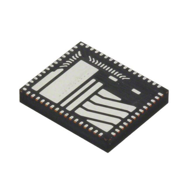
56-pin (10mm x 12mm x 1.85mm) QFN
EVB-EN5395QI
EN5395QI
QFN Evaluation Board
Packing and Marking Information: https://www.altera.com/support/quality-and-reliability/packing.html
PIN FUNCTIONS
Figure 2: Pin Diagram (Top View)
NOTE A: NC pins are not to be electrically connected to each other or to any external signal, ground or voltage. However,
they must be soldered to the PCB. Failure to follow this guideline may result in part malfunction or damage.
Page 2
02392
December 18, 2018
Rev H
�Data Sheet | Intel Enpirion Power Solutions: EN5395QI
PIN DESCRIPTIONS
PIN
1-3
NAME
NC
TYPE
FUNCTION
-
NO CONNECT – This pin should not be electrically connected to any
external signal, voltage, or ground. This pin may be connected internally.
However, this pin must be soldered to the PCB.
4-5
NC(SW)
-
NO CONNECT – These pins are internally connected to the common drain
output of the internal MOSFETs. NC(SW) pins are not to be electrically
connected to any external signal, ground, or voltage. However, they must
be soldered to the PCB. Failure to follow this guideline may result in part
malfunction or damage.
6-13
NC
-
NO CONNECT – This pin should not be electrically connected to any
external signal, voltage, or ground. This pin may be connected internally.
However, this pin must be soldered to the PCB.
14-20
VOUT
Power
Regulated converter output. Connect these pins to the load and place
output capacitor from these pins the PGND pins 24-26.
21-22
NC(SW)
-
NO CONNECT – These pins are internally connected to the common drain
output of the internal MOSFETs. NC(SW) pins are not to be electrically
connected to any external signal, ground, or voltage. However, they must
be soldered to the PCB. Failure to follow this guideline may result in part
malfunction or damage.
23
NC
-
NO CONNECT – This pin should not be electrically connected to any
external signal, voltage, or ground. This pin may be connected internally.
However, this pin must be soldered to the PCB.
24-29
PGND
Power
Output power ground. Refer to layout guideline section.
30-35
PVIN
Power
Input power supply. Connect to input power supply. Decouple with input
capacitor to PGND.
36-37
NC
-
NO CONNECT – This pin should not be electrically connected to any
external signal, voltage, or ground. This pin may be connected internally.
However, this pin must be soldered to the PCB.
38
ROCP
Analog
Optional Over Current Protection adjust pin. Place ROCP resistor
between this pin and AGND (pin 40) to adjust the over current trip point.
39
AVIN
Power
Analog voltage input for the controller circuits. Connect this pin to the
input power supply.
40
AGND
Power
Analog ground for the controller circuits.
41-42
NC
-
NO CONNECT – This pin should not be electrically connected to any
external signal, voltage, or ground. This pin may be connected internally.
However, this pin must be soldered to the PCB.
43
VS2
Analog
Voltage select line 2 input. See Table 1.
44
VS1
Analog
Voltage select line 1 input. See Table 1.
45
VS0
Analog
Voltage select line 0 input. See Table 1.
46
POK
Digital
Power OK is an open drain transistor for power system state indication.
POK is a logic high when VOUT is with -10% to +20% of VOUT nominal.
Page 3
02392
December 18, 2018
Rev H
�Data Sheet | Intel Enpirion Power Solutions: EN5395QI
PIN
NAME
TYPE
FUNCTION
47
VSENSE
Analog
Remote voltage sense input. Connect this pin to the load voltage at the
point to be regulated.
48
SS
Analog
Soft-Start node. The soft-start capacitor is connected between this pin
and AGND. The value of this capacitor determines the startup timing.
49
EAIN
Analog
Optional Error Amplifier input. Allows for customization of the control
loop.
50
EAOUT
Analog
Optional Error Amplifier output. Allows for customization of the control
loop.
51
COMP
Analog
Output of the buffer leading to the error amplifier. Used for external
modifications of the compensation network.
52
ENABLE
Analog
Input Enable. Applying a logic high, enables the output and initiates a
soft-start. Applying a logic low disables the output.
Analog
PWM input/output. Used for optional master/slave configuration. When
M/S pin is asserted “low”, PWM will output the gate-drive PWM
waveform. When the M/S pin is asserted “high”, the PWM pin is
configured as an input for PWM signal from the “master” device. PWM
pin can drive up to 3 slave devices.
-
NO CONNECT – This pin should not be electrically connected to any
external signal, voltage, or ground. This pin may be connected internally.
However, this pin must be soldered to the PCB.
53
54
PMW
NC
55
M/S
Analog
Optional Master/Slave select pin. Asserting pin “low” places device in
Master Mode for current sharing. PWM pin (53) will output PWM drive
signal. Asserting pin “high” will place the device in Slave Mode. PWM pin
(53) will be configured to input (receive) PWM drive signal from “Master”
device.
56-58
NC
-
NO CONNECT – Do not electrically connect these pins to each other or to
PCB. CAUTION! May be internally connected.
Page 4
02392
December 18, 2018
Rev H
�Data Sheet | Intel Enpirion Power Solutions: EN5395QI
ABSOLUTE MAXIMUM RATINGS
CAUTION: Absolute Maximum ratings are stress ratings only. Functional operation beyond the recommended
operating conditions is not implied. Stress beyond the absolute maximum ratings may impair device
life. Exposure to absolute maximum rated conditions for extended periods may affect device reliability.
Absolute Maximum Pin Ratings
PARAMETER
SYMBOL
MIN
MAX
UNITS
PVIN
-0.5
7.0
V
ENABLE, VSENSE, VS0-VS2, M/S
-0.5
VIN
V
EAIN, EAOUT, COMP
-0.5
2.5
V
SS, PWM
-0.5
3.0
V
POK
-0.5
VIN +0.3
V
MIN
MAX
UNITS
+150
°C
+150
°C
+260
°C
MAX
UNITS
Absolute Maximum Thermal Ratings
PARAMETER
CONDITION
Maximum Operating Junction
Temperature
Storage Temperature Range
Reflow Peak Body Temperature
-65
(10 Sec) MSL3 JEDEC J-STD020A
Absolute Maximum ESD Ratings
PARAMETER
CONDITION
MIN
HBM (Human Body Model)
±2000
V
CDM (Charged Device Model)
±500
V
RECOMMENDED OPERATING CONDITIONS
PARAMETER
SYMBOL
MIN
MAX
UNITS
VIN
2.375
5.5
V
Output Voltage Range
VOUT
0.75
VIN – VDO (1)
V
Output Current Range
IOUT
0
Operating Ambient Temperature Range
TA
Operating Junction Temperature
TJ
Input Voltage Range
(2)
9
A
-40
+85
°C
-40
+125
°C
Page 5
02392
December 18, 2018
Rev H
�Data Sheet | Intel Enpirion Power Solutions: EN5395QI
THERMAL CHARACTERISTICS
PARAMETER
SYMBOL
TYPICAL
UNITS
TSD
150
°C
TSDHYS
20
°C
Thermal Resistance: Junction to Ambient (0 LFM) (3)
θJA
18
°C/W
Thermal Resistance: Junction to Case (0 LFM)
θJC
1.5
°C/W
Thermal Overload Trip Point
Thermal Overload Trip Point Hysteresis
(1) VDO (dropout voltage) is defined as (ILOAD x Droput Resistance). Please refer to Electrical Characteristics Table.
(2) Reference figures 5 and 6 fir the Output Current Derating Curves.
(3) Based on four layer board and proper thermal design in line with JEDEC EIJ/JESD 51 standards.
ELECTRICAL CHARACTERISTICS
NOTE: VIN = 5.5V, Minimum and Maximum values are over operating ambient temperature range unless
otherwise noted. Typical values are at TA = 25°C.
PARAMETER
SYMBOL
TEST CONDITIONS
MIN
TYP
MAX
UNITS
TA = 25C, 2.375V ≤ VIN ≤ 5.5V
ILOAD = 1A; TA = 25°C
VOUT Initial Accuracy
∆VOUT_INIT
%
VID Output Voltage Setting (V):
1.2, 1.25, 1.5, 1.8, 2.5, 3.3
-2
+2
0.8
-3
+3
2.4V ≤ VIN ≤ 5.5V
-40°C ≤ TA ≤ +85°C
Overall VOUT Accuracy
(Line, Load, and
Temperature
combined)
∆VOUT_ALL
Transient Response
Peak Deviation
∆VOUT
0A ≤ ILOAD ≤ 9A
%
VID Output Voltage Setting (V):
1.2, 1.25, 1.5, 1.8, 2.5, 3.3
-3
+3
0.8
-4
+4
(IOUT = 0% to 100% or 100% to
0% or rated load)
VIN = 5V, 1.2V ≤ VOUT ≤ 3.3V
5
%
COUT = 2 x 47 μF
Under Voltage Lock
out threshold
VUVLO
VIN Increasing
2.2
VIN Decreasing
2.1
V
Page 6
02392
December 18, 2018
Rev H
�Data Sheet | Intel Enpirion Power Solutions: EN5395QI
PARAMETER
Switching Frequency
SYMBOL
TEST CONDITIONS
MIN
FSWITCH
TYP
MAX
5
UNITS
MHz
2.375V ≤ VIN ≤ 5.5V
Continuous Output
Current
0.603


 工商网监
湘ICP备2023018690号
工商网监
湘ICP备2023018690号
