Enpirion® Power Evaluation Board User Guide
EN5364QI PowerSoC
Enpirion EN5364QI 6A DCDC Converter
w/Integrated Inductor Evaluation Board
Introduction
Thank you for choosing Altera Enpirion power products!
This user guide should be used together with the latest device datasheet.
•
•
The EN5364QI features integrated inductor, power MOSFETS, Controller,
bulk of the compensation Network, and protection circuitry against system
faults. This level of integration delivers a substantial reduction in footprint
and part count over competing solutions. However, the evaluation board is
not optimized for minimum footprint; rather for engineering ease of
evaluation through programming options, clip leads, test points etc.
The EN5364QI device is feature rich and supports the following additional
functions:
o Margining – The output voltage can be changed by ±2.5%, ±5% or
±10% about the nominal, under digital control using ternary pins
MAR[1:2] Margining is highly valued for system robustness
verification and reliability studies. Note: POK automatically scales
with margining.
o Phase Lock - The internal switching frequency can be phase
locked to an external clock source (or another EN5364QI) by
connecting such a clock source to pin S_IN. This feature is highly
valued to keep beat frequencies (between a system sampling clock
and the DC/DC converter switching frequency) out of the desired
signal band.
o Delay - A delayed version of the internal switching clock (or the
PWM signal) is available at pin S_OUT. This may be input to
another EN5364QI device.
o The delay is programmable by means of a single resistor
connected between pin S_delay and AGND. This feature allows the
control of input ripple when multiple EN5364QI devices are used on
a system board.
o Pre-bias operation – When the device pre-bias is enabled (jumper
provided), the device will monotonically ramp-up its output voltage
from a pre-bias voltage level to the programmed output voltage
level under control of Enable signal. The pre-bias (Back-feed)
voltage may be coupled to the output via a diode. This diode (D2) is
populated on the board. Back-feed voltage may be applied at
BF_IN (TP18)
Page 1 of 11
www.altera.com/enpirion
�Enpirion® Power Evaluation Board User Guide
EN5364QI PowerSoC
•
•
•
•
•
o Parallel Mode operation – Up to 4 EN5364QI devices may be
operated in parallel when load currents greater than 6A is desired.
In parallel mode, one device is designated the Master and up to 3
devices operate in slave mode, controlled by the Master. The PWM
output of the Master is routed to slave devices. By daisy chaining
the Slave devices even more devices can be operated in parallel
but practical considerations, such as board layout would limit the
number of slave devices to three.
o Soft-Start – A 15nF (C11) soft-start capacitor is populated on the
evaluation board for an output voltage ramp time of ~1ms. This may
be swapped for a different value capacitor if a different ramp time is
desired. To limit the inrush current this capacitor value should be
greater than 4.7nF. The output voltage rise time is ~65k*CSS.
The EN5364QI features a customer programmable output voltage by
means of a resistor divider. The resistor divider allows the user to set the
VOUT to any value within the range 0.6V to approximately (VIN-0.5V).
`Referring to Figure 1, the evaluation board, as shipped is populated with
a single RA, a single CA, and four possible RB resistors. A jumper selects
one of the 4 RB resistors to produce a voltage of 0.804, 0.998, 1.2 or
1.8Volts. You can populate more than one RB jumper position to get even
higher output voltages. See “VOUT Programming” section in the
evaluation board schematic (Figure 7).
The EN5364QI includes the bulk of the compensation network internally.
However, an external phase-lead (zero) capacitor is required as part of the
feedback. This network is shown in Figure -1. Appropriate component
values allow for optimum compensation for a given Input voltage and
choice of loop bandwidth. The equations in Figure 1 provide the details to
calculate component values.
MAR1 and MAR2 are ternary input signals. The pins are allowed to be in a
low state (tied to GND), a high state (tied to VIN), or a float state. Table-1
shows the margining truth table. Accordingly, the output voltage can be
nominal or ±2.5%, ±5% or ±10% about the nominal. 7 out of 9 possible
states of MAR[1:2] are used for margining. The other two states are
reserved for diagnostics. If tying MAR[1,2] to VIN, a series resistor is
recommended to reduce the pin input current (see Figure 2).
A footprint is provided for a SMC connector (not populated) for S_IN. A
clock source (3.6 to 4.4MHz) may be applied to S_IN to synchronize the
device switching frequency to the external source. S_OUT will output a
clock signal synchronous with the switching frequency, with a phase
delay. S_OUT of one EN5364QI may be connected to S_IN of another
EN5364QI device in different modes of operation.
The phase delay is set by connecting a resistor from S_delay to AGND.
The delay is approximately:
Delay (nsec) = 2*[S_delay resistance in kΩ.]
Page 2 of 11
www.altera.com/enpirion
�Enpirion® Power Evaluation Board User Guide
EN5364QI PowerSoC
•
•
•
A 49.9kΩ (populated on Evaluation board) resistor value delays the clock
signal by ~100nsec.
EN5364QI supports pre-bias mode operation. To use this option set the
EN_PB jumper to pre-bias enable position with device powered down.
When the device is subsequently powered and enabled, the output
voltage will ramp monotonically from its pre-bias value to the programmed
value. Pre-bias voltage may be applied to clip lead BF_IN on the
evaluation board. A diode D2 is populated on the board between BF_IN
and VOUT.
Jumpers are provided for ease of logical high/low programming of the
following signals:
o Enable
o Pre-bias Enable
o MAR1 and MAR2 Margining ternary inputs
o Master/Slave ternary input
Enable may also be controlled using an external switching source by
removing the jumper and applying the enable signal to the middle pin and
ground.
o Jumpers are also provided for selecting one of 4 possible output
voltages.
The board comes with input decoupling and reverse polarity protection to
guard the device against common setup mishaps.
VOUT
RA
RB
CA
VFB
RA = 30,000 × Vin (value in Ω)
4.72 × 10 −6
CA =
RA
(C A in Farads,
RA in Ω)
RB =
VFB × RA
(VOUT − VFB )
Figure - 1 : Output voltage programming and loop compensation. RA and CA
correspond R17 & C20 on the board. RB corresponds to a combination of
R13, R14, R16, or R18 on the board, depending on which jumpers are
populated on J13.
Page 3 of 11
www.altera.com/enpirion
�Enpirion® Power Evaluation Board User Guide
EN5364QI PowerSoC
2.5V
R1
100k
Rext
To Gates
250
VIN
D1
R2
100k
Vf ~ 2V
R3
3k
AGND
IC Package
Figure 2: Equivalent circuit of a ternary pin
(MAR1, MAR2, or M/S) input buffer. To get a
logic High on a ternary input, pull the pin to VIN
through an external resistor REXT. The board is
populated with a 10kΩ REXT for all three ternary
pins.
Quick Start Guide
GND
SIDE
VIN
SIDE
Figure – 3 : J1 Mode Selection Jumpers
In Figure 3, the jumper on ENA pin as shown is in disable mode. For all the J1
positions, when the jumper is between the middle and right pins the signal pin is
connected to ground or logic low. When the jumper is between the left and
middle pins, the signal pin is connected to VIN or logic High. When there is no
jumper, MAR1, MAR2 and M_S pins will be in Float mode, however ENA and
EN_PB are internally pulled low.
WARNING: complete steps 1 through 4 before applying power to the EN5364QI
evaluation board.
STEP 1: Set the “ENA” and “ENA_PB” jumper to the Disable Position. Select
MAR1, MAR2, and M/S to float (no jumper).
STEP 2: Set the output voltage select jumper for the desired setting as shown
below:
Figure – 4 : J13 Voltage Selection Jumpers
Page 4 of 11
www.altera.com/enpirion
�Enpirion® Power Evaluation Board User Guide
EN5364QI PowerSoC
In Figure 4, output Voltages, from left to right, are 0.804V, 0.998V, 1.2V
and 1.0V.Jumper as shown, selects 1.2V output. Higher output voltages
can be achieved by populating multiple J13 jumper positions. See Figures
1 and 7.
CAUTION: Except for ENA, NONE of the J1 & J13 jumpers can be
changed while the EN5364QI is enabled. Doing so could damage the part.
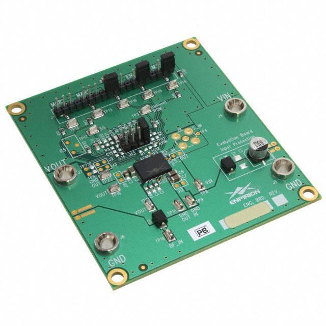
STEP 3: Connect Power Supply to the input power connectors, VIN (+) and
GND (−) as indicated in Figure - 5 and set the power supply to the desired
voltage. The compensation components for the board have been optimized for
an input voltage of 5V (see Figures 1 & 7). To optimize the board for another
input voltage, calculate new values RA, CA, and RB using the equations in Figure
1. The caption in Figure 1, states which components on the PCB correspond to
RA , CA , & RB .
CAUTION: be mindful of the polarity. Even though the evaluation board
comes with reverse polarity protection diodes, it is rarely a good idea to
reverse the input polarity.
STEP 4: Connect the load to the output connectors VOUT (+) and GND (−), as
indicated in Figure -5.
STEP 5: Power up the board and move the ENA jumper to the enabled position.
The EN5364QI is now powered up and generating the desired output. You are
free to make Efficiency, Ripple, Line/Load Regulation, Load transient, Power OK,
over current limit and temperature related measurements. You may also view the
delayed switching clock at S_OUT. However, you do not have a reference to
measure the delay against!
STEP 5A: Power Up/Down Behavior – Remove ENA jumper and connect a
pulse generator (output disabled) signal to the middle pin of ENA and Ground.
Set the pulse amplitude to swing from 0 to 2.5 volts. Set the pulse period to
10msec., duty cycle to 50% and fast transition (