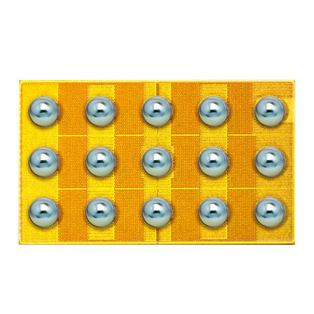
EPC2049 – Enhancement-Mode Power Transistor
Preliminary Specification Sheet
Status: Engineering
Features:
• VDS, 40 V
• Maximum RDS(on), 5 mΩ
• ID, 16 A
Applications:
• Point of Load Converters
• Envelope Tracking Power Supplies
• LiDAR/Pulsed Power Applications
• Class D Audio
• Low Inductance Motor Drive
EPC2049 eGaN® FETs are supplied in
passivated die form with solder bumps.
Die Size: 2.5 mm x 1.5 mm
Maximum Ratings
Drain-to-Source Voltage (Continuous)
40
Drain-to-Source Voltage (up to 10,000 5ms pulses at 150˚C)
48
ID
Continuous (TA = 25˚C, RθJA= 8 ˚C/W)
Pulsed (25˚C, TPULSE = 300 µs)
16
175
A
VGS
Gate-to-Source Voltage
Gate-to-Source Voltage
6
-4
V
TJ
TSTG
Operating Temperature
Storage Temperature
-40 to 150
-40 to 150
˚C
VDS
V
Static Characteristics (TJ= 25˚C unless otherwise stated)
PARAMETER
TEST CONDITIONS
BVDSS
Drain-to-Source Voltage
VGS = 0 V, ID = 0.5 mA
IDSS
Drain Source Leakage
VDS = 32 V, VGS = 0 V
MIN
TYP
MAX
UNIT
0.1
0.4
mA
mA
mA
40
V
Gate-to-Source Forward Leakage
VGS = 5 V
0.5
5.5
Gate-to-Source Reverse Leakage
VGS = -4 V
0.1
0.4
VGS(TH)
Gate Threshold Voltage
VDS = VGS, ID = 6 mA
1.4
2.5
V
RDS(on)
VSD
Drain-Source On Resistance
Source-Drain Forward Voltage
VGS = 5 V, ID = 15 A
IS = 0.5 A, VGS = 0 V
4.3
2
5
mΩ
IGSS
0.8
V
Thermal Characteristics
TYP
UNIT
RθJC
Thermal Resistance, Junction to Case
1.4
˚C/W
RθJB
Thermal Resistance, Junction to Board
8.5
˚C/W
RθJA
Thermal Resistance, Junction to Ambient (Note 1)
64
˚C/W
Note 1: RθJA is determined with the device mounted on one square inch of copper pad, single layer 2 oz copper on FR4 board.
See http://epc-co.com/epc/documents/product-training/Appnote_Thermal_Performance_of_eGaN_FETs.pdf for details.
Subject to Change without Notice
www.epc-co.com
COPYRIGHT 2017
Page 1
�EPC2049 – Enhancement-Mode Power Transistor
Preliminary Specification Sheet
Dynamic Characteristics (TJ= 25˚C unless otherwise stated)
PARAMETER
TEST CONDITIONS
MIN
TYP
MAX
670
805
CISS
Input Capacitance
CRSS
Reverse Transfer Capacitance
COSS
Output Capacitance
350
COSS(ER)
Effective Output Capacitance,
Energy Related (note 2)
551
COSS(TR)
Effective Output Capacitance,
Time Related (note 3)
RG
Gate Resistance
QG
Total Gate Charge
QGS
Gate-to-Source Charge
QGD
Gate-to-Drain Charge
QG(TH)
12
VDS = 20 V, VGS = 0 V
VDS = 0 to 20 V, VGS = 0 V
Output Charge
QRR
Source-Drain Recovery Charge
525
pF
623
0.6
VDS = 20 V, VGS = 5 V, ID=15 A
6.1
Ω
7.6
2.1
1.1
VDS = 20 V, ID = 15 A
Gate Charge at Threshold
QOSS
UNIT
nC
1.5
VDS = 20 V, VGS = 0 V
13
20
0
Note 2: COSS(ER) is a fixed capacitance that gives the same stored energy as COSS while VDS is rising from 0 to 50% BVDSS.
Note 3: COSS(TR) is a fixed capacitance that gives the same charging time as COSS while VDS is rising from 0 to 50% BVDS.
Figure 1: Typical Output Characteristics at 25°C
Subject to Change without Notice
www.epc-co.com
Figure 2: Transfer Characteristics
COPYRIGHT 2017
Page 2
�EPC2049 – Enhancement-Mode Power Transistor
Preliminary Specification Sheet
Figure 3: RDS(on) vs VGS for Various Drain Currents
Figure 4: RDS(on) vs VGS for Various Temperatures
Figure 5a: Capacitance (Linear Scale)
Figure 5b: Capacitance (Log Scale)
Figure 5c: Output Charge and COSS Stored Energy
Figure 6: Gate Charge
Subject to Change without Notice
www.epc-co.com
COPYRIGHT 2017
Page 3
�EPC2049 – Enhancement-Mode Power Transistor
Preliminary Specification Sheet
Figure 7: Reverse Drain-Source Characteristics
Figure 8: Normalized On-State Resistance vs Temperature
Figure 9: Normalized Threshold Voltage vs Temperature
Figure 10: Safe Operating Area
Subject to Change without Notice
www.epc-co.com
COPYRIGHT 2017
Page 4
�EPC2049 – Enhancement-Mode Power Transistor
Preliminary Specification Sheet
Figure 11a: Transient Thermal Response Curves (Junction-to-Case)
Notes:
Duty Factor: D = t1/t2
Peak TJ = PDM x ZθJC x RθJC + TC
Figure 11b: Transient Thermal Response Curves (Junction-to-Board)
Notes:
Duty Factor: D = t1/t2
Peak TJ = PDM x ZθJB x RθJB + TB
Subject to Change without Notice
www.epc-co.com
COPYRIGHT 2017
Page 5
�EPC2049 – Enhancement-Mode Power Transistor
Preliminary Specification Sheet
DIE MARKINGS
EPC2045 (note 1)
DIE OUTLINE
Solder Bar View
DIM
MICROMETERS
MIN
Nominal
MAX
A
2470
2500
2530
B
1470
1500
1530
c
450
d
500
e
238
264
290
Side View
Subject to Change without Notice
www.epc-co.com
COPYRIGHT 2017
Page 6
�EPC2049 – Enhancement-Mode Power Transistor
Preliminary Specification Sheet
RECOMMENDED LAND PATTERN
(measurements in µm)
The land pattern is solder mask defined
Solder mask is 10μm smaller per side than bump
DIM
MICROMETERS
A
2500
B
1500
c
450
d
500
f
230
RECOMMENDED STENCIL DRAWING
(measurements in µm)
g
7
10
13
2
5
8
11
14
3
6
9
12
15
B
4
c
1
h
A
DIM
MICROMETERS
A
2500
B
1500
c
450
d
500
g
300
h
250
Recommended stencil should be 4mil (100µm)
thick, must be laser cut, openings per drawing.
The corner has a radius of R60
Intended for use with SAC305 Type 4
solder, reference 88.5% metals content.
Additional assembly resources available at epcco.com/epc/DesignSupport/AssemblyBasics.aspx
d
Efficient Power Conversion Corporation (EPC) reserves the right to make changes without further notice to any products herein. Engineering devices, designated with an
ENG* suffix at point of purchase, are first article products that EPC is preparing for production release. Specifications may change on final production release of the
device. If you have questions please contact us. EPC does not assume any liability arising out of the application or use of any product or circuit described herein; neither
does it convey any license under its patent rights, nor the rights of other.
eGaN® is a registered trademark of Efficient Power Conversion Corporation.
EPC Patents: http://epc-co.com/epc/AboutEPC/Patents.aspx
Subject to Change without Notice
www.epc-co.com
Revised January 2019
COPYRIGHT 2017
Page 7
�
很抱歉,暂时无法提供与“EPC2049ENGRT”相匹配的价格&库存,您可以联系我们找货
免费人工找货