Development Board
EPC9003C
Quick Start Guide
200 V Half-bridge with Gate Drive, Using EPC2010C
Revision 4.1
�QUICK START GUIDE
EPC9003C
DESCRIPTION
The EPC9003C development board is a 200 V maximum device voltage,
22 A maximum output current, half bridge with onboard gate drives,
featuring the EPC2010C GaN field effect transistor (FET). The purpose
of this development board is to simplify the evaluation process of the
EPC2010C by including all the critical components on a single board that
can be easily connected into the majority of existing converter topologies.
The EPC9003C development board measures 2” x 2” and contains two
EPC2010C GaN FETs in a half bridge configuration with the On-Semi
NCP51820 gate driver. The board also contains all critical components
and the layout supports optimal switching performance. There are also
various probe points to facilitate simple waveform measurement and
efficiency calculation. A block diagram of the circuit is given in figure 1.
For more information on EPC2010C please refer to the datasheet
available from EPC at www.epc-co.com. The datasheet should be read in
conjunction with this quick start guide.
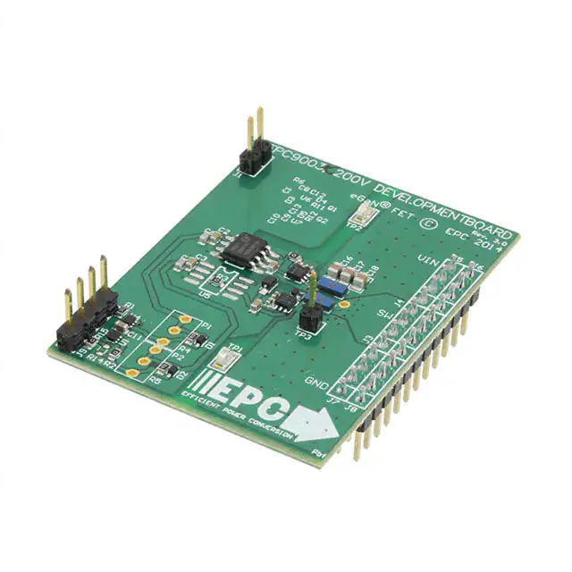
Front view
Table 1: Performance Summary (TA = 25°C) EPC9003C
Symbol
Parameter
VDD
Gate Drive Input
Supply Range
Conditions
10
IOUT
Bus Input Voltage
Range(1)
Switch Node Output
Current (2)
VPWM
PWM Logic Input
Voltage Threshold (3)
VIN
Min Nominal Max Units
Minimum ‘High’ State
Input Pulse Width
Minimum ‘Low’ State
Input Pulse Width (4)
12
V
160
Input ‘High’
3.5
Input ‘Low’
0
VPWM rise and
50
fall time < 10ns
VPWM rise and
200
fall time < 10ns
5
A
5.5
1.5
V
ns
(1) Maximum input voltage depends on inductive loading, maximum switch node ringing
must be kept under 200 V for EPC2010C.
(2) Maximum current depends on die temperature – actual maximum current is affected by
switching frequency, bus voltage and thermal cooling.
(3) When using the on board logic buffers, refer to the NCP51820 datasheet when bypassing the logic buffers.
(4) Limited by time needed to ‘refresh’ high side bootstrap supply voltage.
EPC9003C development board
Back view
DBTST
VDD
Q1
Gate drive
regulator
LDO
EN
PWM
LDO
Logic and
dead-time
adjust
Hin
Lin
DT
Logic
GND
VIN
CBypass
LDO
L1
Level
shift
DC Output
Q2
LDO
Level
shift
Cout
PGND
Gate driver
Figure 1: Block diagram of EPC9003C development board
EPC – POWER CONVERSION TECHNOLOGY LEADER | EPC-CO.COM | ©2022 |
| 2
�QUICK START GUIDE
EPC9003C
QUICK START PROCEDURE
The EPC9003C development board is easy to set up as a buck or boost
converter to evaluate the performance of two EPC2010C eGaN FETs.
In addition to the deadtime features of the NCP51820 gate driver, this board
includes a dead-time generating circuit that adds a delay from when the
gate signal of one FET is commanded to turn off, to when the gate signal
of the other FET is commanded to turn on. In the default configuration, the
NCP51820 gate driver is set mode D (no-dead time, no-cross conduction
protection - refer to datasheet for NCP51820) and the on-board dead time
circuit provides the necessary dead time and ensures that both the high and
low side FETS will not be turned on at the same time thus preventing a shoot
through condition.
Single input
Dual input
Dual-mode dead time settings
Top-side
Bottom-side
Enable
PWM1
(a)
PWM2
(b)
(c)
Figure 2: Input mode selection on J630
Single/dual PWM signal input settings
Note: In dual mode there is no shoot-through protection as both gate
signals can be set high at the same time. 2. The NCP51820 has an on-chip
deadtime generator with several modes of operation. The EPC9003C
disables the on-chip deadtime to maximize end user flexibility, but it
makes the on-chip deadtime modes accessible through P1, R11, and R12.
Refer to the NCP51820 datasheet for details on setting the dead time using
P1, R11 and R12.
Output Capacitor
Buck Inductor
EPC9003C
Rev. 4.1
VDD supply
(Note polarity)
VMain
supply
(Note
polarity)
+
To select dual input mode, the zero-ohm resistor in position R5 needs to be
removed and installed in position R6 as shown in figure 2(b).
12 VDC
+
PWM1 and PWM2. Both input ports are used as inputs in dual-input mode
where PWM1 connects to the upper FET and PWM2 connects to the lower
FET. The PWM1 input port is used as the input in single-input mode where
the circuit will generate the required complementary PWM with preset dead
time for the FETs as shown in figure 2(a). This is the default configuration.
160 VDCmax
PWM1
(default)
+
Switch-node
output
Buck converter configuration
DC load
To operate the board as a buck converter, either a single or dual PWM input
can be chosen. Figure 3(a) shows the connection setup for single PWM
input mode and figure 3(b) for the dual PWM input mode.
(a)
12 VDC
Note: It is important to provide the correct PWM signals that includes
dead-time and polarity when operating in dual PWM input mode and not
making use of the gate driver dead time function.
+
Once the input source and dead-time settings have be chosen and set,
then the board can be operated.
Output Capacitor
Buck Inductor
EPC9003C
Rev. 4.1
VDD supply
(Note polarity)
VMain
supply
(Note
polarity)
2. With power off, connect the switch node (SW) of the half bridge to your
circuit as required (half bridge configuration). Or use the provided pads
for inductor (L1) and output capacitors (Cout), as shown in figure 3.
3. With power off, connect the gate drive supply to VDD (J1, Pin-1) and
ground return to GND (J1, Pin-2 indicated on the bottom side of the
board).
4. With power off, connect the input PWM control signal to PWM1 and/or
PWM2 according to the input mode setting chosen and ground return
to any of GND J10 pins indicated on the bottom side of the board.
5. Turn on the gate drive supply – make sure the supply is at least 10 V but
does not exceed 12 V.
6. Turn on the controller / PWM input source.
7. Making sure the initial input supply voltage is 0 V, turn on the power
and slowly increase the voltage to the required value (do not exceed the
absolute maximum voltage). Probe switching node to see switching
operation.
+
1. With power off, connect the input power supply bus to VIN and ground/
return to GND.
160 VDCmax
PWM1
Upper
FET
PWM2
Lower
FET
+
+
DC load
(b)
Figure 3: (a) Single-PWM input buck converter (b) Dual-PWM input buck converter
configurations showing the supply, output capacitor, inductor, PWM, and load
connections.
8. Once operational, adjust the PWM control, bus voltage, and load
within the operating range and observe the output switching
behavior, efficiency, and other parameters.
9. For shutdown, please follow steps in reverse.
EPC – POWER CONVERSION TECHNOLOGY LEADER | EPC-CO.COM | ©2022 |
| 3
�QUICK START GUIDE
EPC9003C
Boost Converter configuration
To operate the board as a boost converter, either a single or dual
PWM input can be chosen. Figure 4(a) shows the connection setup
for single PWM input mode and figure 4(b) for the dual PWM input
mode.
12 VDC
+
Warning: Never operate the boost converter mode without a
load as the output voltage can increase beyond the maximum
ratings.
Input Capacitor
Boost Inductor
EPC9003C
Rev. 4.1
VDD supply
(Note polarity)
Notes:
DC load
160 VDCmax
1. It is important to provide the correct PWM signals that
includes dead-time and polarity when operating in dual PWM
input mode and not making use of the gate driver dead time
function.
PWM1
+
+
2. Boost mode PWM converters are theoretically capable of
generating arbitrarily high voltages, limited only by losses
and component ratings. Review the operation of boost mode
converters and make sure to avoid combinations of duty cycle
and load that will generate higher voltages than the voltage
rating of the development board and attached components.
VMain supply
(Note polarity)
(a)
Once the input source, dead-time settings and bypass configurations
have be chosen and set then the boards can be operated.
2. With power off, connect the input power supply bus to VOUT
and ground / return to GND, or externally across the capacitor
if the inductor L1 and Cout are provided externally. Connect the
output voltage (labeled as VIN) to your circuit as required, e.g.,
resistive load.
12 VDC
+
1. The inductor (L1) and input capacitors (labeled as Cout) can
either be soldered onto the board, as shown in figure 4, or
provided off board.
Input Capacitor
Boost Inductor
EPC9003C
Rev. 4.1
VDD supply
(Note polarity)
DC load
160 VDCmax
3. With power off, connect the gate drive supply to VDD (J1, Pin-1)
and ground return to GND (J1, Pin-2 indicated on the bottom
side of the board).
5. Turn on the gate drive supply – make sure the supply is at least
10 V but does not exceed 12 V.
PWM1
Upper
FET
PWM2
Lower
FET
+
+
+
4. With power off, connect the input PWM control signal to PWM1
and/or PWM2 according to the input mode setting chosen and
ground return to any of GND J10 pins indicated on the bottom
side of the board.
VMain supply
(Note polarity)
6. Turn on the controller / PWM input source.
7. Making sure the output is not open circuit, and the input
supply voltage is initially 0 V, turn on the power and slowly
increase the voltage to the required value (do not exceed the
absolute maximum voltage). Probe switching node to see
switching operation.
(b)
Figure 4: (a) Single-PWM input boost converter (b) Dual-PWM input
boost converter configurations showing the supply, inductor, input
capacitor, PWM, and load connections.
8. Once operational, adjust the PWM control, bus voltage, and load
within the operating range and observe the output switching
behavior, efficiency, and other parameters. Observe device
temperature for operational limits.
9. For shutdown, please follow steps in reverse.
EPC – POWER CONVERSION TECHNOLOGY LEADER | EPC-CO.COM | ©2022 |
| 4
�QUICK START GUIDE
EPC9003C
MEASUREMENT CONSIDERATIONS
+V
Measurement connections are shown in figure 5.
Figure 6 shows an actual switch-node voltage
measurement when operating the board as a buck
converter.
When measuring the switch node voltage containing
high-frequency content, care must be taken to
provide an accurate high-speed measurement. An
optional two pin header (J5) and an MMCX connector
(J6) are provided for switch-node measurement.
A differential probe is recommended for measuring
the high-side bootstrap voltage. IsoVu probes from
Tektronix has mating MMCX connector.
For regular passive voltage probes (e.g. TPP1000)
measuring switch node using MMCX connector,
probe adaptor is available. PN: 206-0663-xx.
EPC9003C
HIGH VOLTAGE
Rev. 4.1
Upper FET Gate
Voltage MMCX
(HIGH VOLTAGE!)
Voltage measurement:
Input voltage for Buck,
Output voltage for Boost
(HIGH VOLTAGE!)
HIGH VOLTAGE
Lower FET
Gate Voltage
HIGH VOLTAGE
Voltage measurement:
Input voltage for Boost,
Output voltage for Buck
(HIGH VOLTAGE!)
V
+
Switch-node
oscilloscope probe
Ground oscilloscope probe
(a)
PCB#: B5217
NOTE. For information about measurement techniques,
the EPC website offers: “AN023 Accurately Measuring
High Speed GaN Transistors” and the How to GaN
educational video series, including: HTG09- Measurement
HIGH VOLTAGE
Switch-node oscilloscope
probe (HIGH VOLTAGE!)
Rev. 4.1
Ground oscilloscope probe
THERMAL CONSIDERATIONS
Switch-node MMCX
(HIGH VOLTAGE!)
The EPC9003C is intended for bench evaluation
with low ambient temperature and convection
cooling. The addition of a heat-spreader or heatsink
and forced air cooling can significantly increase
the current rating of these devices, but care must
be taken to not exceed the absolute maximum die
temperature of 150°C.
HIGH VOLTAGE
(b)
NOTE. The EPC9003C development board does not have any
current or thermal protection on board. For more information
regarding the thermal performance of EPC eGaN FETs, please
consult: D. Reusch and J. Glaser, DC-DC Converter Handbook,
a supplement to GaN Transistors for Efficient Power
Conversion, First Edition, Power Conversion Publications, 2015.
Figure 5 Measurement points (a) front side, (b) Back side
30 V/div
5 ns/div
tf = 7.5 ns
10%–90%
fall time
tr = 2.4 ns
10%–90%
rise time
Waveform 8 A, VIN = 160 V, VOUT = 28 V, L = 200 kHz
Figure 6: Typical switch-node waveform when operated as a buck converter
EPC – POWER CONVERSION TECHNOLOGY LEADER | EPC-CO.COM | ©2022 |
| 5
�QUICK START GUIDE
EPC9003C
Table 2: Bill of Materials
Item Qty
Reference
Part Description
Manufacturer
Part Number
1
9
C1, C2, C3, C4, C5, C6, C7, C8, C9
0.33 μF 250 V
TDK
CGA6M3X7T2E334K200AA
2
4
C10, C11, C12, C13
0.1 μF 250 V
TDK
C2012X7T2E104K125AA
3
4
C14, C16, C23, C24
1 μF 25 V
TDK
C1608X7R1E105K080AB
4
1
C15
4.7 μF 25 V
TDK
C1608X5R1E475K080AC
5
2
C17, C25
0.1 μF 25 V
TDK
C1608X7R1E104K080AA
6
2
C18, C26
0.1 μF 25 V
TDK
C1005X7R1E104K050BB
7
2
C19, C20
100 pF 50 V
Yageo
CC0402KRX7R9BB101
8
1
C21
0.47 μF 25 V
TDK
C2005X5R1E474K050BB
9
1
C22
15 pF 50 V
TDK
CGA2B2C0G1H150J050BA
10
2
Q1, Q2
200 V 25 mΩ GaN FET
EPC
EPC2010C
11
2
R5, R15
300 Ω
Yageo
RC0603FR-07300RL
12
2
R8, R9
10 k
Yageo
RC0603JR-0710KL
13
4
R3, R4, R7, R10
4.7 Ω
Stackpole
RMCF0402FT4R70
14
1
R12
10 k
Yageo
RC0603JR-0710KL
15
1
R13
2Ω
Stackpole
RMCF0402JT2R00
16
1
R14
1Ω
ROHM
MCR01MRT1JR0
17
1
R20
10 k
Panasonic
ERJ-2RKF1002X
18
5
TP1, TP2, TP3, TP5, TP6
SMD probe loop
Keystone 5015
5015
19
1
D1
600 V 200 mA
Rohm
RFU02VSM6STR
20
2
D5, D15
40 V 30 mA
Diodes Inc.
SDM03U40-7
21
1
U1
600 V HB GaN FET gate driver
On Semiconductor
NCP51820AMNTWG
22
1
U2
2 input AND, TinyLogic, 1.65 V-5.5 V, +-32 mA
Fairchild
NC7SZ08L6X
23
1
U3
2 input NAND, TinyLogic, 1.65 V-5.5 V, +-32 mA Fairchild
NC7SZ00L6X
24
1
J1
2x1 0.1 male vertical through hole
Wurth
61300211121
25
1
J7
2x12 0.1 male vertical through hole
Tyco
4-103185-0-04
26
1
J10
4x1 0.1 male vertical through hole
TE Connectivity
4-103185-0-04
Reference
Part Description
Manufacturer
Part Number
Optional Components
Item
Qty
1
2
R1, R2
0Ω
Stackpole
RMC0402ZT0R00
2
3
4
5
6
7
8
9
1
1
1
3
1
1
1
1
R6
Cout1
EN1
J3, J4, J6
J12
L1
P1
R11
0Ω
Cout_generic
0.1 male vertical 1 position 0.1 pitch
MMCX Jack Vertical SMT 50 Ω
7.62 mm Euro Term
GenericOutputInductor
250 k
R0603-TBD
Stackpole
TBD
Wurth
Molex
Wurth
TBD
Bourns
TBD
RMCF0603ZT0R00
TBD
61300111121
734152063
691216410002
TBD
PV37W254C01B00
TBD
EPC – POWER CONVERSION TECHNOLOGY LEADER | EPC-CO.COM | ©2022 |
| 6
�QUICK START GUIDE
9 VDC - 12 VDC
C1
0.33 μF, 250 V
V DD
2
1
i Net C lass
J1
C15
4.7 μF, 25 V
T P1
C10
0.1 μF, 250 V
C14
1 μF, 25 V
Keystone 5015
2
1
V G2
R2
MMCX
V SW
1
2
0Ω
E MPT Y
E MPT Y
MMCX
vGS2 probe adapter
J5
2
1
E MPT Y
vSW probe adapter
MMCX
V SW
J6
Net C lass
i ClassName: HighVoltageGate
1
2
C16
E MPT Y
T P2
Keystone 5015
R 13
vSW probe holes
1 μF, 25 V
C17
2Ω
5V
Y
B
R8
10 k
5V
1
R 15
300 Ω 1%
C19
100 pF, 50 V
PWM2
U3
NC7SZ 00L 6X
CON4
C26
0.1 μF, 25 V
A
R5
B
300 Ω
D5
40 V 30 mA
SD M03U40
PWM2
R9
10 k
R6
13
15 pF, 50 V
12
D15
40 V 30 mA
SD M03U40
11
C20
100 pF, 50 V
PWM1
10 k
C22
10
V DD
R 12
9
10 k
EN
15
A
VBST
U2
NC7SZ 08L 6X
C21
14
PWM1
HIGH VOLTAGE
600 V, 200 mA
R 20
V DD
PWM1
HI N
1
2
3
0.47 μF, 25 V
C23
R3
P1
250 k
EMPTY
V SW
R7
4.7 Ω
8
C25
0.1 μF, 25 V
T P5
K eystone 5015
i Net C lass
V G2
5V
L1
ClassName: HighVoltage
Q2
E PC2010C
R 10
U1
NCP51820AMNT WG
CW
HOT SURFACE
SW Output
4.7 Ω
6
7
DT
J7B
ATTENTION
R4
5
SGND
Q1
E PC2010C
4.7 Ω
1 μF, 25 V
4
LIN
V G1
4.7 Ω
1Ω
C24
1 μF, 25 V
HIGH VOLTAGE
T P3
Keystone 5015
V OUT
TBD
E MPT Y
V OUT
V OUT
T P6
Keystone 5015
Sync Buck Output
1
2
Cout1
TBD
E MPT Y
R 14
R 11
EMPTY
VIN
D1
0.1 μF, 25 V
E N1
EMPTY SIP1
C18
0.1 μF, 25 V
Main Supply Input
J7A
1
2
3
4
5
6
7
8
1
2
J4
9
10
11
12
13
14
15
16
E MPT Y
J3
vGS1 probe adapter
1
2
3
4
C13 ClassName: HighVoltage
0.1 μF, 250 V
C12
0.1 μF, 250 V
J7C
J12
E MPT Y
7.62 mm Euro Term
17
18
19
20
21
22
23
24
EMPTY
R1 0 Ω
E MPT Y
J10
C11
0.1 μF, 250 V
J2
Net C lass
i ClassName: HighVoltageGate
V G1
V SW
C2
C3
C4
C5
C6
C7
C8
C9
0.33 μF, 250 V 0.33 μF, 250 V 0.33 μF, 250 V 0.33 μF, 250 V 0.33 μF, 250 V 0.33 μF, 250 V 0.33 μF, 250 V 0.33 μF, 250 V
GND
Mode D (default)
0Ω
E MPT Y
FD 1 FD 2 FD 3
PCB Fi ducial
Figure 7: EPC9003C main schematic
ATTENTION
ELECTROSTATIC
SENSITIVE DEVICE
EPC9003C
EPC – POWER CONVERSION TECHNOLOGY LEADER | EPC-CO.COM | ©2022 |
VIN
| 7
�For More Information:
Please contact info@epc-co.com
or your local sales representative
Visit our website:
www.epc-co.com
Sign-up to receive
EPC updates at
bit.ly/EPCupdates
or text “EPC” to 22828
EPC Products are distributed through Digi-Key.
www.digikey.com
Demonstration Board Notification
The EPC9003C board is intended for product evaluation purposes only. It is not intended for commercial use nor is it FCC approved for resale. Replace components on
the Evaluation Board only with those parts shown on the parts list (or Bill of Materials) in the Quick Start Guide. Contact an authorized EPC representative with any questions. This board is
intended to be used by certified professionals, in a lab environment, following proper safety procedures. Use at your own risk.
As an evaluation tool, this board is not designed for compliance with the European Union directive on electromagnetic compatibility or any other such directives or regulations. As board
builds are at times subject to product availability, it is possible that boards may contain components or assembly materials that are not RoHS compliant. Efficient Power Conversion Corporation (EPC) makes no guarantee that the purchased board is 100% RoHS compliant.
The Evaluation board (or kit) is for demonstration purposes only and neither the Board nor this Quick Start Guide constitute a sales contract or create any kind of warranty, whether express
or implied, as to the applications or products involved.
Disclaimer: EPC reserves the right at any time, without notice, to make changes to any products described herein to improve reliability, function, or design. EPC does not assume any liability
arising out of the application or use of any product or circuit described herein; neither does it convey any license under its patent rights, or other intellectual property whatsoever, nor the
rights of others.
�