Figure 4: Typical Waveforms for VIN = 48 V to 5 V/14 A (500 kHz) Buck converter
CH1: Switch node voltage (VSW) - CH2: PWM input voltage (VPWM)
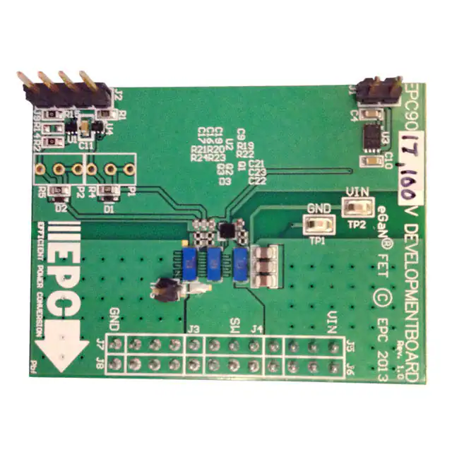
NOTE. The EPC9017 development board does not have any current or thermal protection on board.
Figure 3: Proper Measurement of Switch Node – VSW
EFFICIENT POWER CONVERSION
EPC
The EPC9017 development board showcases the EPC2001 eGaN FET. Although the electrical performance surpasses that for traditional silicon
devices, their relatively smaller size does magnify the thermal management requirements. The EPC9017 is intended for bench evaluation with low
ambient temperature and convection cooling. The addition of heat-sinking and forced air cooling can significantly increase the current rating of
these devices, but care must be taken to not exceed the absolute maximum die temperature of 125°C.
Minimize loop
Place probe
tip on probe
pad at OUT
Ground probe
against TP3
THERMAL CONSIDERATIONS
NOTE. When measuring the high frequency content switch node (OUT), care must be taken to avoid long ground leads. Measure the switch node (OUT) by placing the
oscilloscope probe tip through the large via on the switch node (designed for this purpose) and grounding the probe directly across the GND terminals provided. See
Figure 3 for proper scope probe technique.
1. With power off, connect the input power supply bus to +VIN (J5, J6) and ground / return to –VIN (J7, J8).
2. With power off, connect the switch node of the half bridge OUT (J3, J4) to your circuit as required.
3. With power off, connect the gate drive input to +VDD (J1, Pin-1) and ground return to –VDD (J1, Pin-2).
4. With power off, connect the input PWM control signal to PWM (J2, Pin-1) and ground return to any of the remaining J2 pins.
5. Turn on the gate drive supply – make sure the supply is between 7 V and 12 V range.
6. Turn on the bus voltage to the required value (do not exceed the absolute maximum voltage of 100 V on VOUT).
7. Turn on the controller / PWM input source and probe switching node to see switching operation.
8. Once operational, adjust the bus voltage and load PWM control within the operating range and observe the output switching behavior,
efficiency and other parameters.
9. For shutdown, please follow steps in reverse.
Development board EPC9017 is easy to set up to evaluate the performance of the EPC2001 eGaN FET. Refer to Figure 2 for proper connect
and measurement setup and follow the procedure below:
Do not use probe ground lead
Figure 2: Proper Connection and Measurement Setup
EFFICIENT POWER CONVERSION
EPC
Figure 1: Block Diagram of EPC9017 Development Board
–
(For Efficiency
Measurement)
PWM
Input
VDD
Quick Start Procedure
PWM Input
Logic and
Dead-time
Adjust
–
VIN V
LM5113
Gate
Driver
Gate Drive Gate Drive Supply
Regulator
External Circuit
OUT
VIN
Half-Bridge with Bypass
Switch Node
+
IIN
VIN Supply
+
很抱歉,暂时无法提供与“EPC9017”相匹配的价格&库存,您可以联系我们找货
免费人工找货- 国内价格 香港价格
- 40+1162.4176840+150.57375