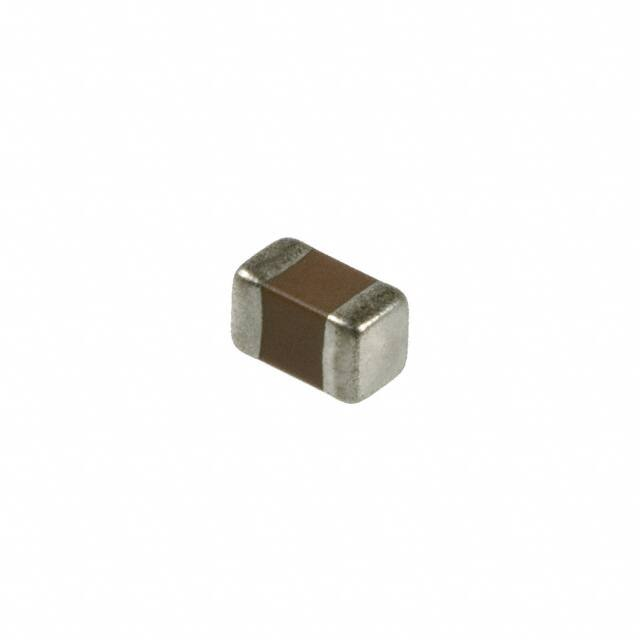
Multilayer Ceramic Capacitors
Series/Type:
B37937, B37947
The following products presented in this data sheet are being withdrawn.
Ordering Code
B37947K9102J060
B37947K9102J070
B37947K9152J060
Substitute Product
Date of Withdrawal
2007-12-21
2007-12-21
2007-12-21
Deadline Last
Orders
2008-03-31
2008-03-31
2008-03-31
Last Shipments
2008-06-30
2008-06-30
2008-06-30
�Ordering Code
B37947K9152J070
B37947K9222J062
B37947K9222J072
B37947K9472J062
B37947K9472J072
B37937K9561J060
B37937K9561J070
B37937K9681J060
B37937K9681J070
B37937K9102J060
B37937K9102J070
B37947K9103G*
B37947K9103F*
B37947K9682G*
B37947K9562J*
B37937K9227J*
B37937K9222G*
B37937K9182J*
B37947K9682J072
B37947K9682J062
B37947K9332J072
B37947K9332J062
B37947K9103J072
B37947K9103J062
B37937K9222J070
B37937K9222J060
B37937K9152J070
B37937K9152J060
Substitute Product
Date of Withdrawal
2007-12-21
2007-12-21
2007-12-21
2007-12-21
2007-12-21
2007-12-21
2007-12-21
2007-12-21
2007-12-21
2007-12-21
2007-12-21
2007-10-26
2007-10-26
2007-10-26
2007-10-26
2007-10-26
2007-10-26
2007-10-26
2007-10-26
2007-10-26
2007-10-26
2007-10-26
2007-10-26
2007-10-26
2007-10-26
2007-10-26
2007-10-26
2007-10-26
Deadline Last
Orders
2008-03-31
2008-03-31
2008-03-31
2008-03-31
2008-03-31
2008-03-31
2008-03-31
2008-03-31
2008-03-31
2008-03-31
2008-03-31
2008-01-31
2008-01-31
2008-01-31
2008-01-31
2008-01-31
2008-01-31
2008-01-31
2008-01-31
2008-01-31
2008-01-31
2008-01-31
2008-01-31
2008-01-31
2008-01-31
2008-01-31
2008-01-31
2008-01-31
Last Shipments
2008-06-30
2008-06-30
2008-06-30
2008-06-30
2008-06-30
2008-06-30
2008-06-30
2008-06-30
2008-06-30
2008-06-30
2008-06-30
2008-04-30
2008-04-30
2008-04-30
2008-04-30
2008-04-30
2008-04-30
2008-04-30
2008-04-30
2008-04-30
2008-04-30
2008-04-30
2008-04-30
2008-04-30
2008-04-30
2008-04-30
2008-04-30
2008-04-30
For further information please contact your nearest EPCOS sales office, which will also support you in selecting a
suitable substitute. The addresses of our worldwide sales network are presented at www.epcos.com/sales.
�Multilayer ceramic capacitors
Chip
CPPS
Ordering code system
B37937
K
9
102
J
0
60
Packaging
60
62
70
72
^
^
^
^
cardboard tape, 180-mm reel
blister tape, 180-mm reel
cardboard tape, 330-mm reel
blister tape, 330-mm reel
Internal coding
Capacitance tolerance
J ^ ± 5% (standard)
K ^ ±10%
Capacitance, coded
(example)
Rated voltage
Termination
102 ^ 10 · 102 pF = 1 nF
103 ^ 10 · 103 pF = 10 nF
Rated voltage [VDC]
Code
16
9
K ^ nickel barrier for all case sizes
Type and size
Chip size
(inch / mm)
Temperature characteristic
CPPS
0603 / 1608
0805 / 2012
B37937
B37947
Please read Cautions and warnings and
Important notes at the end of this document.
2
10/06
�Chip
Multilayer ceramic capacitors
CPPS
Features
■
■
■
■
■
■
■
Replacement of PPS film capacitors
Class 1 characteristic with high capacitance values
High insulation resistance
Excellent DC characteristic
Excellent temperature characteristic
No piezoelectric effects
No ageing effects
Applications
■
■
■
■
■
Wireless communication
Loop filter
PLL filter
Telecom (mobile phones, Bluetooth, ADSL/XDSL)
Automotive (keyless entry)
Termination
■ For soldering: Nickel barrier terminations (Ni)
Options
■ Alternative capacitance tolerances available on request
Delivery mode
■ Cardboard and blister tape (blister tape for chip thickness ³1.2 ± 0.1 mm),
180-mm and 330-mm reel available
Electrical data
Temperature characteristic
Climatic category (IEC 60068-1)
Standard
Dielectric
Rated voltage
Test voltage
Capacitance range / E series
Temperature coefficient
Dissipation factor (limit value)
Insulation resistance1) at + 25 °C
Insulation resistance1) at +125 °C
Time constant1) at + 25 °C
Time constant1) at +125 °C
Operating temperature range
Ageing
VR
Vtest
CR
tan d
Rins
Rins
t
t
Top
1) For CR >10 nF the time constant t = C · Rins is given.
Please read Cautions and warnings and
Important notes at the end of this document.
3
10/06
C0G
55/125/56
EIA
Class 1
16
2.5 · VR/5 s
560 pF … 10 nF (E6)
0 ± 30 · 10 –6/K
105
>104
>1000
>100
–55 … +125
none
VDC
VDC
MW
MW
s
s
°C
�Multilayer ceramic capacitors
CPPS
CPPS
Capacitance tolerances
Code letter
J
(standard)
K
Tolerance
± 5%
±10%
Dimensional drawing
s
b
k
k
KKE0329-N
Dimensions (mm)
Case size
(inch)
(mm)
0603
1608
0805
2012
l
1.6 ± 0.15
2.00 ± 0.20
b
0.8 ± 0.10
1.25 ± 0.15
s
0.8 ± 0.10
1.30 max.
k
0.1 –0.40
0.13 –0.75
Tolerances to CECC 32101-801
Please read Cautions and warnings and
Important notes at the end of this document.
4
10/06
�Multilayer ceramic capacitors
CPPS
CPPS
Recommended solder pad
C
A
D
KKE0308-1
Recommended dimensions (mm) for reflow soldering
Case size
(inch/mm)
Type
A
C
D
0603/1608
0805/2012
single chip
single chip
0.6 … 0.7
0.6 … 0.7
1.8 … 2.2
2.2 … 2.6
0.6 … 0.8
0.8 … 1.1
Termination
Termination
(nickel barrier)
Ceramic body
Inner electrode
Substrate electrode
Intermediate electrode
External electrode
AgPd
Ag
Ni
Sn
KKE0484-W
Please read Cautions and warnings and
Important notes at the end of this document.
5
10/06
�CPPS
Multilayer ceramic capacitors
CPPS
Product range for CPPS chip capacitors
Size1)
inch
mm
Type
VR (VDC)
CR
0603
1608
0805
2012
B37937
B37947
16
16
560. pF
680. pF
1.0 nF
1.5 nF
2.2 nF
3.3 nF
4.7 nF
6.8 nF
10. nF
1) l ´ b (inch) / l ´ b (mm)
Please read Cautions and warnings and
Important notes at the end of this document.
6
10/06
�Multilayer ceramic capacitors
CPPS
CPPS; 0603 and 0805
Ordering codes and packing for CPPS capacitors, 16 VDC, nickel barrier terminations
mm
Cardboard tape,
Æ 180-mm reel
** ^ 60
pcs/reel
Cardboard tape,
Æ 330-mm reel
** ^ 70
pcs/reel
0.8 ± 0.1
0.8 ± 0.1
0.8 ± 0.1
0.8 ± 0.1
0.8 ± 0.1
4000
4000
4000
4000
4000
16000
16000
16000
16000
16000
0.6 ± 0.1
0.8 ± 0.1
1.2 ± 0.1
1.2 ± 0.1
1.2 ± 0.1
1.2 ± 0.1
1.2 ± 0.1
5000
4000
3000 3)
3000 3)
3000 3)
3000 3)
3000 3)
20000
16000
12000 4)
12000 4)
12000 4)
12000 4)
12000 4)
Chip thickness
CR1)
Ordering code 2)
Case size 0603, 16 VDC
560. pF
680. pF
1.0 nF
1.5 nF
2.2 nF
B37937K9561J0**
B37937K9681J0**
B37937K9102J0**
B37937K9152J0**
B37937K9222J0**
Case size 0805, 16 VDC
1.0 nF
1.5 nF
2.2 nF
3.3 nF
4.7 nF
6.8 nF
10. nF
B37947K9102J0**
B37947K9152J0**
B37947K9222J0**
B37947K9332J0**
B37947K9472J0**
B37947K9682J0**
B37947K9103J0**
1) Other capacitance values on request.
2) The table contains the ordering codes for the standard capacitance tolerance.
For other available capacitance tolerances see page 168.
3) Blister tape, 180-mm reel, ordering code ** ^ 62
4) Blister tape, 330-mm reel, ordering code ** ^ 72
Please read Cautions and warnings and
Important notes at the end of this document.
7
10/06
�CPPS
Multilayer ceramic capacitors
CPPS
Typical characteristics 1)
Capacitance change DC/C25 versus
temperature T (tolerance range
)
Capacitance change DC/C0 versus
superimposed DC voltage V
KKE0483-N
0.5
∆C %
C 25
KKE0460-J
0.5
0.3
∆C %
C0
0.3
0.2
0.2
0.1
0.1
0
0
_ 0.1
_ 0.1
_ 0.2
_ 0.2
_ 0.3
_ 0.3
_ 0.4
_ 0.4
_ 0.5
_ 55 _ 40 _ 20 0
20 40 60 80
˚C
_ 0.5
120
0
2
4
6
8
10
T
12
14 V 16
V
Dissipation factor tan d versus
temperature T
Impedance |Z| versus
frequency f
KKE0488-U
10 3
10
_2
KKE0118-V
Ω
tan δ
Z
10
2
10
1 nF
_3
10 1
4.7 nF
10 0
10
10 nF
10
10
_4
_1
_2
10 0
10 1
10 2
10
MHz 10 3
f
_5
_ 60 _ 40 _ 20 0 20 40 60 80 100 C 140
˚
T
1) For more detailed information on frequency behavior and characteristics see www.epcos.com/mlcc_impedance.
Please read Cautions and warnings and
Important notes at the end of this document.
8
10/06
�Multilayer ceramic capacitors
CPPS
CPPS
Typical characteristics 1)
Capacitance change DC/C1 versus
time t
Insulation resistance Rins versus
temperature T
KKE0129-B
10 8
MΩ
KKE0100-S
5
∆C %
C1
0
R ins
10 6
_5
10 5
_ 10
10 4
_ 15
10 3
10 2
0
20
40
60
80
100
_ 20
10 0
˚C 140
T
10 1
10 2
h 10 3
t
1) For more detailed information on frequency behavior and characteristics see www.epcos.com/mlcc_impedance.
Please read Cautions and warnings and
Important notes at the end of this document.
9
10/06
�Multilayer ceramic capacitors
Cautions and warnings
Notes on the selection of ceramic capacitors
In the selection of ceramic capacitors, the following criteria must be considered:
1. Depending on the application, ceramic capacitors used to meet high quality requirements should
at least satisfy the specifications to AEC-Q200. They must meet quality requirements going
beyond this level in terms of ruggedness (e.g. mechanical, thermal or electrical) in the case of
critical circuit configurations and applications (e.g. in safety-relevant applications such as ABS
and airbag equipment or durable industrial goods).
2. At the connection to the battery or power supply (e.g. clamp 15 or 30 in the automobile) and at
positions with stranding potential, to reduce the probability of short circuits following a fracture,
two ceramic capacitors must be connected in series and/or a ceramic capacitor with integrated
series circuit should be used. The MLSC from EPCOS contains such a series circuit in a single
component.
3. Ceramic capacitors with the temperature characteristics Z5U and Y5V do not satisfy the requirements to AEC-Q200 and are mechanically and electrically less rugged than C0G or X7R/X8R
ceramic capacitors. In applications that must satisfy high quality requirements, therefore, these
capacitors should not be used as discrete components (see the chapter “Effects on mechanical,
thermal and electrical stress”, point 1.4).
4. For ESD protection, preference should be given to the use of multilayer varistors (MLV) (see the
chapter “Effects on mechanical, thermal and electrical stress”, point 1.4).
5. An application-specific derating or continuous operating voltage must be considered in order to
cushion (unexpected) additional stresses (see the chapter “Reliability”).
The following should be considered in circuit board design
1. If technically feasible in the application, preference should be given to components having an
optimal geometrical design.
2. At least FR4 circuit board material should be used.
3. Geometrically optimal circuit boards should be used, ideally those that cannot be deformed.
4. Ceramic capacitors must always be placed a sufficient minimum distance from the edge of the
circuit board. High bending forces may be exerted there when the panels are separated and during further processing of the board (such as when incorporating it into a housing).
5. Ceramic capacitors should always be placed parallel to the possible bending axis of the circuit
board.
6. No screw connections should be used to fix the board or to connect several boards. Components should not be placed near screw holes. If screw connections are unavoidable, they must
be cushioned (for instance by rubber pads).
10
10/06
�Multilayer ceramic capacitors
Cautions and warnings
The following should be considered in the placement process
1. Ensure correct positioning of the ceramic capacitor on the solder pad.
2. Caution when using casting, injection-molded and molding compounds and cleaning agents,
as these may damage the capacitor.
3. Support the circuit board and reduce the placement forces.
4. A board should not be straightened (manually) if it has been distorted by soldering.
5. Separate panels with a peripheral saw, or better with a milling head (no dicing or breaking).
6. Caution in the subsequent placement of heavy or leaded components (e.g. transformers or
snap-in components): danger of bending and fracture.
7. When testing, transporting, packing or incorporating the board, avoid any deformation of the
board not to damage the components.
8. Avoid the use of excessive force when plugging a connector into a device soldered onto the
board.
9. Ceramic capacitors must be soldered only by the mode (reflow or wave soldering) permissible
for them (see the chapter “Soldering directions”).
10. When soldering the most gentle solder profile feasible should be selected (heating time, peak
temperature, cooling time) in order to avoid thermal stresses and damage.
11. Ensure the correct solder meniscus height and solder quantity.
12. Ensure correct dosing of the cement quantity.
13. Ceramic capacitors with an AgPd external termination are not suited for the lead-free solder
process: they were developed only for conductive adhesion technology.
This listing does not claim to be complete, but merely reflects the experience of EPCOS AG.
11
10/06
�Multilayer ceramic capacitors
Important notes
The following applies to all products named in this publication:
1. Some parts of this publication contain statements about the suitability of our products for
certain areas of application. These statements are based on our knowledge of typical
requirements that are often placed on our products in the areas of application concerned. We
nevertheless expressly point out that such statements cannot be regarded as binding
statements about the suitability of our products for a particular customer application. As
a rule, EPCOS is either unfamiliar with individual customer applications or less familiar with them
than the customers themselves. For these reasons, it is always ultimately incumbent on the
customer to check and decide whether an EPCOS product with the properties described in the
product specification is suitable for use in a particular customer application.
2. We also point out that in individual cases, a malfunction of passive electronic components
or failure before the end of their usual service life cannot be completely ruled out in the
current state of the art, even if they are operated as specified. In customer applications
requiring a very high level of operational safety and especially in customer applications in which
the malfunction or failure of a passive electronic component could endanger human life or health
(e.g. in accident prevention or life-saving systems), it must therefore be ensured by means of
suitable design of the customer application or other action taken by the customer (e.g.
installation of protective circuitry or redundancy) that no injury or damage is sustained by third
parties in the event of malfunction or failure of a passive electronic component.
3. The warnings, cautions and product-specific notes must be observed.
4. In order to satisfy certain technical requirements, some of the products described in this
publication may contain substances subject to restrictions in certain jurisdictions (e.g.
because they are classed as “hazardous”). Useful information on this will be found in our
Material Data Sheets on the Internet (www.epcos.com/material). Should you have any more
detailed questions, please contact our sales offices.
5. We constantly strive to improve our products. Consequently, the products described in this
publication may change from time to time. The same is true of the corresponding product
specifications. Please check therefore to what extent product descriptions and specifications
contained in this publication are still applicable before or when you place an order.
We also reserve the right to discontinue production and delivery of products.
Consequently, we cannot guarantee that all products named in this publication will always be
available.
6. Unless otherwise agreed in individual contracts, all orders are subject to the current version
of the “General Terms of Delivery for Products and Services in the Electrical Industry”
published by the German Electrical and Electronics Industry Association (ZVEI).
7. The trade names EPCOS, EPCOS-JONES, Baoke, CeraDiode, CSSP, MLSC, PhaseCap,
PhaseMod, SIFERRIT, SIFI, SIKOREL, SilverCap, SIMID, SIOV, SIP5D, SIP5K, UltraCap,
WindCap are trademarks registered or pending in Europe and in other countries. Further
information will be found on the Internet at www.epcos.com/trademarks.
12
10/06
�


 工商网监
湘ICP备2023018690号
工商网监
湘ICP备2023018690号
