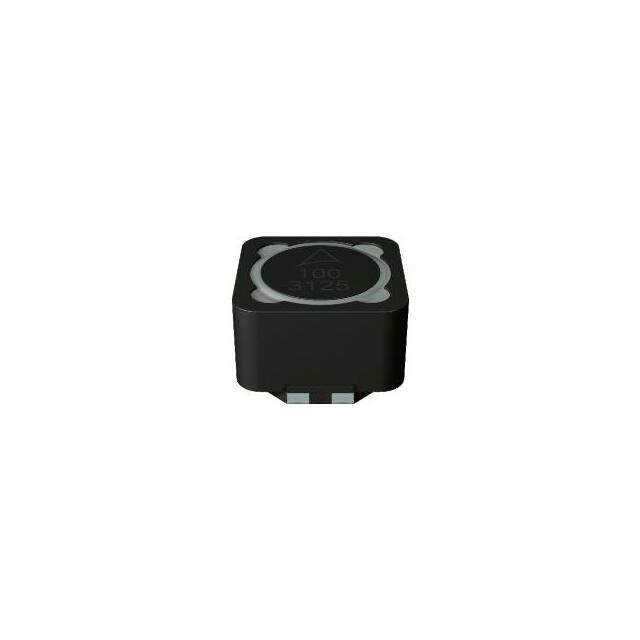
SMT power inductors
Size 12.5 x 12.5 x 8.5 mm
Series/Type:
Ordering code:
B82477D4
Date:
Version:
June 2013
Content of header bars 1 and 2 of data sheet will be automatically entered in headers and footers! Please fill in the
table and then change the color to "white". This ensures that the table disappears (invisible) for the customer PDF.
Don't change formatting when entering or pasting text in the table and don't add any cell or line in and to it!
Identification/Classification 1
(header 1 + top left bar):
SMT power inductors
Identification/Classification 2
(header 2 + bottom left header bar):
Size 12.5 x 12.5 x 8.5 mm
Ordering code: (top right header bar)
Series/Type: (bottom right header bar)
B82477D4
Preliminary data (optional):
(if necessary)
Department:
MAG IN PD
EPCOS AG 2015. Reproduction, publication and dissemination
of this publication, enclosures hereto and the information
Date:
June 2013
contained therein without EPCOS' prior express consent is prohibited.
Version:
EPCOS AG is a TDK Group Company.
02
�SMT power inductors
Size 12.5 x 12.5 x 8.5 mm
B82477D4
Rated inductance 2 ... 100µH
Construction
■ Ferrite core
■ Magnetically shielded
■ Winding: enamel copper wire
■ Winding soldered to terminals
■ Special winding technology for low stray
inductance and high coupling factor
Features
■ High rated current, low DC resistance
■ Temperature range up to +150 °C
■ Suitable for lead-free reflow soldering
as referenced in JEDEC J-STD 020D
■ Qualified to AEC-Q200
■ RoHS-compatible
■ Coupling factor of typically 99% in average
Applications
■ Common mode choke
■ DC/DC converters, especially for SEPIC topology
■ 1:1 transformer
Terminals
■ Base material CuSn6P
■ Layer composition Ni, Sn (lead-free)
■ Electro-plated
Marking
■ Marking on component:
Manufacturer, L value (in µH), Date code
■ Minimum data on reel:
Manufacturer, ordering code, L value,
quantity, date of packing
Delivery mode and packing unit
■ 24-mm blister tape, wound on 330-mm ∅reel
■ Packing unit: 350 pcs./reel
MAG IN PD
Please read Cautions and warnings and
Important notes at the end of this document.
June 2013
Page 2 of 7
�SMT power inductors
Size 12.5 x 12.5 x 8.5 mm
B82477D4
Dimensional drawing and circuit diagram
(Dimensions in mm)
Taping and packing
Direction of unreeling
(Dimensions in mm)
A:330±2
N:75±1
W1:24.4 typ
W2:30.4 max
MAG IN PD
Please read Cautions and warnings and
Important notes at the end of this document.
June 2013
Page 3 of 7
�SMT power inductors
Size 12.5 x 12.5 x 8.5 mm
B82477D4
Technical data and measuring conditions
Rated inductance L1, L2
Leakage or stray inductance Ls
Measured with LCR meter Agilent 4284A at frequency fL,
0.1 V, +20 °C.
Test L1-3 :(short 2+4) .Measured with LCR meter Agilent 4284A
at 100khz, 0.1 V, +20 °C.
Ls
Ln
Coupling factor Ktyp
Coupling in between the 2 windings. k 1
Operating temperature range
–55°C to +150 °C
Rated current IR
Max. permissible DC with temperature increase of ≤40 K
Saturation current ISat
DC with inductance decrease ∆L/L0 of approx. 10%
DC resistance R1,R2 , (max)
Measured at +20 °C
Solderability (lead-free)
Dip and look method Sn95.5Ag3.8Cu0.7:
+(245 5) °C, (3 0.3) s
Wetting of soldering area 90%
(based on IEC 60068-2-58)
Resistance to soldering heat
+260 °C, 40 s (as referenced in JEDEC J-STD-020D)
Climatic category
55/150/56 (to IEC 60068-1)
Storage conditions
Mounted: –55 °C … +150 °C
Packaged: –25 °C … +40 °C, ≤75% RH
Weight
Approx. 4.2 g
MAG IN PD
Please read Cautions and warnings and
Important notes at the end of this document.
June 2013
Page 4 of 7
�SMT power inductors
Size 12.5 x 12.5 x 8.5 mm
B82477D4
Characteristics and ordering codes
L1, L2
Ls,typ K,typ
µH
uH
Tolerance fL
Isat,typ
Isat,min
IR
R1, R2/mΩ
Ordering code
2.0 0.20 94.9
MHz A
15
3.0 0.25 95.7
12
10.25
5.50
22
18.1
B82477D4302M000
4.7 0.25 97.3
10
8.75
5.00
26
23.2
B82477D4472M000
B82477D4682M000
%
A
A
13
5.75
20
16.5
B82477D4202M000
max
typ
6.8 0.25 98.1
8.25
7.25
4.15
35
28.5
0.25 98.7
6.50
5.75
3.75
42
35.5
B82477D4103M000
5.50
4.80
3.25
60
52.5
B82477D4153M000
4.50
4.00
2.80
78
69.5
B82477D4223M000
2.30
110
96.4
B82477D4333M000
10
22
0.30 99.0 ±20% ≙
M
0.30 99.3
33
0.35 99.5
3.80
3.30
47
0.45 99.5
3.30
3.10
1.85
68
0.50 99.6
2.50
2.30
100
0.60 99.7
2.20
2.00
15
0.1
145
115
B82477D4473M000
1.55
215
190
B82477D4683M000
1.35
280
267
B82477D4104M000
Inductance is per winding. When leads are connected in parallel, inductance is the same value. When leads are
connected in series, inductance is four times the value.
DCR is for each winding. When leads are connected in parallel, DCR is half the value. When leads are
connected in series, DCR is twice the value.
Isat ist the current flowing through one winding. When leads are connected in parallel, Isat is the same. When
leads are connected in series, Isat is half the value.
IR is the total current through both windings
I1 and I2 can be calculated like this: I12+I22=IR2
Current derating Iop/IR versus ambient temperature TA
MAG IN PD
Please read Cautions and warnings and
Important notes at the end of this document.
June 2013
Page 5 of 7
�SMT power inductors
Size 12.5 x 12.5 x 8.5 mm
B82477D4
Cautions and warnings
■ Please note the recommendations in our Inductors data book (latest edition) and in the data
sheets.
– Particular attention should be paid to the derating curves given there.
– The soldering conditions should also be observed. Temperatures quoted in relation to wave
soldering refer to the pin, not the housing.
■ If the components are to be washed varnished it is necessary to check whether the washing
varnish agent that is used has a negative effect on the wire insulation, any plastics that are used,
or on glued joints. In particular, it is possible for washing varnish agent residues to have a
negative effect in the long-term on wire insulation.
■ The following points must be observed if the components are potted in customer applications:
– Many potting materials shrink as they harden. They therefore exert a pressure on the plastic
housing or core. This pressure can have a deleterious effect on electrical properties, and in
extreme cases can damage the core or plastic housing mechanically.
– It is necessary to check whether the potting material used attacks or destroys the wire
insulation, plastics or glue.
– The effect of the potting material can change the high-frequecy behaviour of the components.
■ Ferrites are sensitive to direct impact. This can cause the core material to flake, or lead to
breakage of the core.
■ Even for customer-specific products, conclusive validation of the component in the circuit can
only be carried out by the customer.
MAG IN PD
Please read Cautions and warnings and
Important notes at the end of this document.
June 2013
Page 6 of 7
�Important notes
The following applies to all products named in this publication:
1. Some parts of this publication contain statements about the suitability of our products for certain areas
of application. These statements are based on our knowledge of typical requirements that are often placed
on our products in the areas of application concerned. We nevertheless expressly point out that such
statements cannot be regarded as binding statements about the suitability of our products for a
particular customer application. As a rule we are either unfamiliar with individual customer applications or
less familiar with them than the customers themselves. For these reasons, it is always ultimately incumbent
on the customer to check and decide whether a product with the properties described in the product
specification is suitable for use in a particular customer application.
2. We also point out that in individual cases, a malfunction of electronic components or failure before
the end of their usual service life cannot be completely ruled out in the current state of the art, even
if they are operated as specified. In customer applications requiring a very high level of operational safety
and especially in customer applications in which the malfunction or failure of an electronic component could
endanger human life or health (e.g. in accident prevention or life-saving systems), it must therefore be
ensured by means of suitable design of the customer application or other action taken by the customer (e.g.
installation of protective circuitry or redundancy) that no injury or damage is sustained by third parties in the
event of malfunction or failure of an electronic component.
3. The warnings, cautions and product-specific notes must be observed.
4. In order to satisfy certain technical requirements, some of the products described in this publication
may contain substances subject to restrictions in certain jurisdictions (e.g. because they are
classed as hazardous). Useful information on this will be found in our Material Data Sheets on the Internet
(www.tdk-electronics.tdk.com/material). Should you have any more detailed questions, please contact our
sales offices.
5. We constantly strive to improve our products. Consequently, the products described in this publication
may change from time to time. The same is true of the corresponding product specifications. Please
check therefore to what extent product descriptions and specifications contained in this publication are still
applicable before or when you place an order.
We also reserve the right to discontinue production and delivery of products. Consequently, we
cannot guarantee that all products named in this publication will always be available. The aforementioned
does not apply in the case of individual agreements deviating from the foregoing for customer-specific
products.
6. Unless otherwise agreed in individual contracts, all orders are subject to our General Terms and
Conditions of Supply.
7. Our manufacturing sites serving the automotive business apply the IATF 16949 standard. The IATF
certifications confirm our compliance with requirements regarding the quality management system in the
automotive industry. Referring to customer requirements and customer specific requirements (“CSR”) TDK
always has and will continue to have the policy of respecting individual agreements. Even if IATF 16949
may appear to support the acceptance of unilateral requirements, we hereby like to emphasize that only
requirements mutually agreed upon can and will be implemented in our Quality Management
System. For clarification purposes we like to point out that obligations from IATF 16949 shall only become
legally binding if individually agreed upon.
8. The trade names EPCOS, CeraCharge, CeraDiode, CeraLink, CeraPad, CeraPlas, CSMP, CTVS,
DeltaCap, DigiSiMic, ExoCore, FilterCap, FormFit, LeaXield, MiniBlue, MiniCell, MKD, MKK, MotorCap,
PCC, PhaseCap, PhaseCube, PhaseMod, PhiCap, PowerHap, PQSine, PQvar, SIFERRIT, SIFI, SIKOREL,
SilverCap, SIMDAD, SiMic, SIMID, SineFormer, SIOV, ThermoFuse, WindCap are trademarks registered
or pending in Europe and in other countries. Further information will be found on the Internet at www.tdkelectronics.tdk.com/trademarks.
Release 2018-10
Page 7 of 7
�


 工商网监
湘ICP备2023018690号
工商网监
湘ICP备2023018690号
