Real time clock module SERIAL-INTERFACE REAL TIME CLOCK MODULE WITH SRAM
RTC-4553
Product number (please refer to page 2)
Q41 4 5 5 3 5 x x x x x 0 0
• Built-in crystal unit allows adjustment-free efficient operation. • Automatic calendar function (year, month, day, day of the week, hour, minute, second). • Automatic leap year correction. • Builtin 30 x 4-bit S-RAM. • Reference pulse output. (1024 Hz, 1/10 Hz)
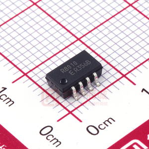
Actual size
The details are mentioned in the application manual.
http://www.epsondevice.com
Specifications (characteristics) Absolute Max. rating
Item Supply voltage Input voltage Output voltage Storage temperature Symbol VDD VIN VOUT TSTG Condition VDD to GND Min. Max. +6.0 -0.3 VDD+0.3 +125 V Unit
Terminal connection RTC-4553
#14 #8
No. Pin terminal GND 1 WR 2 SIN 3 SCK 4 L1 5 L2 6 L3 7 No. Pin terminal 14 TPOUT SOUT 13 CS1 12 CS0 11 L5 10 L4 9 VDD 8
SIN,SCK, WR, CS0, CS1 ____
SOUT, TPOUT
Stored as bare product after unpacking
__ __ __
-55
°C
Operating range
Item Power voltage Clock voltage Symbol VDD VCLK TOPR Condition — — Min. 2.7 2.0 -30 Typ. 5.0 — — Max. 5.5 5.5 +70 Unit V V ˚C
#1
#7
L1 to L5 are test pin. Do not connect them to any terminals.
Operating temperature
No condensation
External dimensions RTC-4553 (SOP 14-pin)
(Unit: mm)
Item
Symbol
Condition Ta=+25 °C, AA A B
Range 5±5 5±10 5±20 3.0 Max. +10 -120
Unit
Frequency tolerance
∆f/fo
VDD=5 V
x 10-6
10.1±0.2
Oscillation start-up time Frequency temperature characteristics
Frequency voltage characteristics Aging
tSTA Top f/V fa
Ta=+25 °C, VDD = 3.0 V
s
3.1 3.2±0.1
Ta=-10 °C to +70 °C, VDD=5 V Reference at +25 °C Ta=Fix, VDD=2 V to 5.5 V
Reference at 5 V
Ta=+25 °C, VDD=5 V, first year
x 10-6 ±5
x 10-6/ year
7.4±0.2
Frequency characteristics
R4553 A E 123 4A
5.0
0.05 Min. 1.27 0.35 0.6
0.15
Metal may be exposed on the top or bottom of this product. This won't affect any quality, reliability or electrical spec.
DC characteristics
Item Symbol IDD1 IDD2 Output voltage VOH VOL IOZH Off leak current IOZL VIH Input voltage VIL IIH Input current IIL
(GND=O V, VDD=5 V ± 10 % , Ta=-30 °C to +70 °C)
Block diagram
32.768 kHz OSC Counter Output control
Day
___
Condition
Min. —
Typ. — 1.0
Max. 100 3.0 — 0.4 2.0
Unit µA
Sec. Min. Hou. of
Week
Day Mon. Year
Current consumption
SCK=500 kHz
___
SCK=O Hz
TP OUT
IOH=-400 µA IOL=1.6 mA VOUT=5.5 V
VDD-0. 4
— -2.0
V
Control register 1
Control register 2
Control register 3
RAM (120bit)
µA
S OUT Output control
VOUT=0 V
4/5 VDD
— — VIN=5.5 V -2.0 VIN=0 V
—
—
V
SCK S IN CS 1 CS 0 WR
1/5 VDD
2.0 µA
Input control
Shift register Control circuit
83
�THE CRYSTALMASTER
ENERGY SAVING EPSON
EPSON offers effective savings to its customers through a wide range of electronic devices, such as semiconductors, liquid crystal display (LCD) modules, and crystal devices. These savings are achieved through a sophisticated melding of three different efficiency technologies. Power saving technology provides low power consumption at low voltages. Space saving technology provides further reductions in product size and weight through super-precise processing and high-density assembly technology. Time saving technology shortens the time required for design and development on the customer side and shortens delivery times. Our concept of Energy Saving technology conserves resources by blending the essence of these three efficiency technologies. The essence of these technologies is represented in each of the products that we provide to our customers. In the industrial sector, leading priorities include measures to counter the greenhouse effect by reducing CO2, measures to preserve the global environment, and the development of energy-efficient products. Environmental problems are of global concern, and although the contribution of energy-saving technology developed by EPSON may appear insignificant, we seek to contribute to the development of energy-saving products by our customers through the utilization of our electronic devices. EPSON is committed to the conservation of energy, both for the sake of people and of the planet on which we live.
WORKING WITH ENVIRONMENTAL ISSUES
In 1988, Seiko Epson led in working to abolish CFCs, and perfect abolition of those ozone layer-destroying substances was achieved in 1992. In 1998, the 10th year of start of the CFC-free activity, Seiko Epson set this year as the "Second Environmental Benchmark Year" and established a new corporate General Environmental Policy. Seiko Epson is tackling with environmental issues comprehensively. At the end of Fiscal 1988, Seiko Epson succeeded in abolishing chloric solvents doubted to be harmful to human body. In fiscal 1999, Seiko Epson started the activity with a goal of abolishing lead solder pointed out possibility of enironmental pollutant.
Co-existence Mark
The environmental mark symbolizing Epson's basic stance of "Co-existence with Nature". The design incorporates a fish, flower, and water, representing mutually supportive coexistence.
Promotion of Environment Management System conforming to International Standard
To strengthen management for environmental activities, Seiko Epson Group aims at acquisition of the ISO14001 certification for Japanese and abroad main business bases (including affiliates) for manufacturing, sales, software development and others. As of May 25 , 2001, planned 68 bases of all manufacturing bases and some non-manufacturing bases have acquired the certification.
ISO14000 is an international standard for environmental management that was established by the International Standards Organization in 1996 against the background of growing concern regarding global warming, destruction of the ozone layer, and global deforestation.
WORKING FOR HIGH QUALITY
Seiko-Epson quickly began working to acquire company-wide ISO9000 series certification, and has acquired ISO9001 or ISO9002 certification with all targeted products manufactured in Japanese and overseas plants. The Quartz Device Operations Division, EPM and SZE have acquired QS-9000 certification, which are of higher level.
QS-9000: This is an enhanced standard for quality assurance systems formulated by leading U.S. automobile manufacturers based on the international ISO 9000 series.
NOTICE
• The material is subject to change without notice. • Any part of this material may not be reproduced or duplicated in any form or any means without the written permission of Seiko Epson. • The information, applied circuit, program, using way etc., written in this material is just for reference. Seiko Epson does not assume any liability for the occurrence of infringing any patent or copyright of third party. This material does not authorize the licence for any patent or intellectual property rights. • Any product described in this Foreign Exchange and Foreign Trade Law of Japan and may require an export licence from the Ministry of International Trade and industry or other approval from another government agency. • The products (excert for some product for automotive applications) listed up on this material are designed to be used with ordinary electronic equipment (OA equipment, AV equipment, communications equipment, measuring instruments etc). Seiko Epson does not assume any liability for the case using the products with the application required high reliability or safty extremely (such as aerospace equipment etc). When intending to use any our product with automotive application and the other application than ordinary electronic equipments as above, please contact our sales representatives in advance.
�