S1D13513 Display Controller
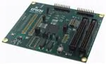
S5U13513P00C100 Evaluation Board
User Manual
Document Number: X78A-G-003-01
Status: Revision 1.1
Issue Date: 2010/09/06
© SEIKO EPSON CORPORATION 2006-2010. All Rights Reserved.
Information in this document is subject to change without notice. You may download and use this document, but only for your own use in
evaluating Seiko Epson/EPSON products. You may not modify the document. Epson Research and Development, Inc. disclaims any
representation that the contents of this document are accurate or current. The Programs/Technologies described in this document may contain
material protected under U.S. and/or International Patent laws.
EPSON is a registered trademark of Seiko Epson Corporation. All other trademarks are the property of their respective owners.
Revision 1.1
�Page 2
Epson Research and Development
Vancouver Design Center
S1D13513
X78A-G-003-01
S5U13513P00C100 Evaluation Board User Manual
Issue Date: 2010/09/06
Revision 1.1
�Epson Research and Development
Vancouver Design Center
Page 3
Table of Contents
1
Introduction . . . . . . . . . . . . . . . . . . . . . . . . . . . . . . . . . . . . . . . . 5
2
Features . . . . . . . . . . . . . . . . . . . . . . . . . . . . . . . . . . . . . . . . . . 6
3
Installation and Configuration . . . . . . . . . . . . . . . . . . . . . . . . . . . . . . 7
3.1 Configuration DIP Switch . . . . . . . . . . . . . . . . . . . . . . . . . . . 7
3.2 Configuration Jumpers . . . . . . . . . . . . . . . . . . . . . . . . . . . 10
4
Technical Description . . . . . . . . . . . . . . . . . . . . . . . . .
4.1 Power . . . . . . . . . . . . . . . . . . . . . . . . . .
4.1.1 Power Requirements . . . . . . . . . . . . . . . . . . . . . . . .
4.1.2 Voltage Regulators . . . . . . . . . . . . . . . . . . . . . . . . .
4.1.3 S1D13513 Power . . . . . . . . . . . . . . . . . . . . . . . . . .
4.2 Clocks . . . . . . . . . . . . . . . . . . . . . . . . . .
4.3 Reset . . . . . . . . . . . . . . . . . . . . . . . . . . .
4.4 Host Interface . . . . . . . . . . . . . . . . . . . . . . .
4.4.1 Connecting to the Epson S5U13U00P00C100 USB Adapter Board
4.4.2 Connecting to the Epson PC Card Extender Board . . . . . . . . .
4.4.3 Direct Host Bus Interface Support . . . . . . . . . . . . . . . . .
4.5 LCD Panel Interface . . . . . . . . . . . . . . . . . . . . .
4.6 Camera Interface . . . . . . . . . . . . . . . . . . . . . .
4.7 YUV Output for TV Display . . . . . . . . . . . . . . . . .
4.8 Keypad Interface . . . . . . . . . . . . . . . . . . . . . .
4.9 PWM Outputs . . . . . . . . . . . . . . . . . . . . . . .
4.10 GPIO Connections . . . . . . . . . . . . . . . . . . . . .
4.11 JTAG Connector . . . . . . . . . . . . . . . . . . . . . .
5
Parts List . . . . . . . . . . . . . . . . . . . . . . . . . . . . . . . . . . . . . . . . 21
6
Schematic Diagrams . . . . . . . . . . . . . . . . . . . . . . . . . . . . . . . . . . 24
7
S5U13513P00C100 Board Layout . . . . . . . . . . . . . . . . . . . . . . . . . . . 28
8
References . . . . . . . . . . . . . . . . . . . . . . . . . . . . . . . . . . . . . . . 30
8.1 Documents . . . . . . . . . . . . . . . . . . . . . . . . . . . . . . . 30
8.2 Document Sources . . . . . . . . . . . . . . . . . . . . . . . . . . . . 30
9
Technical Support . . . . . . . . . . . . . . . . . . . . . . . . . . . . . . . . . . . 31
9.1 EPSON Display Controllers (S1D13513) . . . . . . . . . . . . . . . . . . . . 31
9.2 Ordering Information . . . . . . . . . . . . . . . . . . . . . . . . . . . 31
S5U13513P00C100 Evaluation Board User Manual
Issue Date: 2010/09/06
.
.
.
.
.
.
.
.
.
.
.
.
.
.
.
.
.
.
. . . . . . .
. . . . . .
. . . . . . . .
. . . . . . . .
. . . . . . . .
. . . . . .
. . . . . .
. . . . . .
. . . . . . . .
. . . . . . . .
. . . . . . . .
. . . . . .
. . . . . .
. . . . . .
. . . . . .
. . . . . .
. . . . . .
. . . . . .
13
13
13
13
13
14
14
15
15
15
16
17
18
19
19
19
19
20
S1D13513
X78A-G-003-01
Revision 1.1
�Page 4
Epson Research and Development
Vancouver Design Center
S1D13513
X78A-G-003-01
S5U13513P00C100 Evaluation Board User Manual
Issue Date: 2010/09/06
Revision 1.1
�Epson Research and Development
Vancouver Design Center
Page 5
1 Introduction
This manual describes the setup and operation of the S5U13513P00C100 Evaluation
Board. The evaluation board is designed as an evaluation platform for the S1D13513
Display Controller.
The S5U13513P00C100 evaluation board can connect to the S5U13U00P00C100 USB
Adapter board so that it can be used with a laptop or desktop computer, via USB 2.0. With
some minor modifications, it is possible to connect the S5U13513P00C100 evaluation
board to a Epson PC Card Extender board instead of a USB Adapter board. The
S5U13513P00C100 evaluation board can also be used with many other native platforms via
the host connectors which provide the appropriate signals to support a variety of CPUs.
This user manual is updated as appropriate. Please check the Epson Research and Development Website at www.erd.epson.com for the latest revision of this document before
beginning any development.
We appreciate your comments on our documentation. Please contact us via email at
documentation@erd.epson.com.
S5U13513P00C100 Evaluation Board User Manual
Issue Date: 2010/09/06
S1D13513
X78A-G-003-01
Revision 1.1
�Page 6
Epson Research and Development
Vancouver Design Center
2 Features
The S5U13513P00C100 Evaluation Board includes the following features:
• 256-pin PBGA S1D13513 Display Controller
• On-board SDRAM, selectable as 8MB x 32-bit or 8MB x 16-bit
• Headers for connection to the S5U13U00P00C100 USB Adapter board or to the PC
Card Extender board
• Headers for connecting to various Host Bus Interfaces
• Headers for connecting to LCD panels
• Headers for connecting to cameras
• On-board 10MHz crystal (used for OSC1 clock input)
• On-board 27MHz crystal (used for OSC2 clock input)
• 14-pin DIP socket (used to install an oscillator for CLKI3 clock input)
• 3.3V input power
• On-board voltage regulator with 1.8V output
S1D13513
X78A-G-003-01
S5U13513P00C100 Evaluation Board User Manual
Issue Date: 2010/09/06
Revision 1.1
�Epson Research and Development
Vancouver Design Center
Page 7
3 Installation and Configuration
The S5U13513P00C100 evaluation board incorporates a DIP switch, jumpers, and 0 ohm
resistors which allow it to be used with a variety of different configurations.
3.1 Configuration DIP Switch
The S1D13513 has configuration inputs (CNF[8:0]) which are read on the rising edge of
RESET#. A 10-position DIP switch (SW1) is used to configure the S1D13513 for multiple
Host Bus Interfaces. The following figure shows the location of DIP switch SW1 on the
S5U13513P00C100.
DIP SWITCH - SW1
Figure 3-1: Configuration DIP Switch (SW1) Location
All S1D13513 configuration inputs (CNF[8:0]) are fully configurable using DIP switch
SW1 as described below.
Table 3-1: Summary of Power-On/Reset Options
SDU13513B00C
SW1-[10:1] Config
S1D13513
CNF[8:0] Config
SW1-[10]
-
SW1-[9:8]
Power-On/Reset State
1 (ON)
Not used
CNF[8:7]
SW1-[6]
CNF5
SW1-[7]
CNF6
SW1-[5:1]
CNF[4:0]
0 (OFF)
00b
CLKI3 is the PLL1 clock source
01b
BUSCLK is the PLL1 clock source
10b
OSC1 is the PLL1 clock source
11b
OSC2 is the PLL1 clock source
Direct access
Indirect access
See Table 3-2: “CNF[4:0] Setting
for CNF[6] = 1b”
00000b
See Table 3-3: “CNF[4:0] Setting for
CNF[6] = 0b”
Parallel Direct 80 Type 2: 1CS#
(see Table 3-2: “CNF[4:0] Setting for CNF[6] = 1b” )
= Required settings when using S5U13U00P00C100 USB Adapter board (SW1-[9:1] = 101000000b)
S5U13513P00C100 Evaluation Board User Manual
Issue Date: 2010/09/06
S1D13513
X78A-G-003-01
Revision 1.1
�Page 8
Epson Research and Development
Vancouver Design Center
Table 3-2: CNF[4:0] Setting for CNF[6] = 1b
CNF[4:0]
Host Bus
00000b
Parallel Direct 80 Type 2: 1 CS#
00001b
Reserved
00010b
Parallel Indirect 80 Type 2
00011b
Reserved
00100b
Parallel Direct 80 Type 1: 1 CS#
00101b
Parallel Direct 68: 1 CS#
00110b
Parallel Indirect 80 Type 1
00111b
Parallel Indirect 68
01000b
Parallel Direct 80 Type 2: 2 CS#
01001b
Reserved
01010b
Reserved
01011b
Reserved
01100b
Parallel Direct 80 Type 1: 2 CS#
01101b
Parallel Direct 68: 2 CS#
01110b
Reserved
01111b
Reserved
10000b
Serial on HVDD1: Data valid on falling edge
10001b
Serial on HVDD2: Data valid on falling edge
10010b
Reserved
10011b
Reserved
10100b
Reserved
10101b
Reserved
10110b
Reserved
10111b
Reserved
11000b
Serial on HVDD1: Data valid on rising edge
11001b
Serial on HVDD2: Data valid on rising edge
11010b
Reserved
11011b
Reserved
11100b
Reserved
11101b
Reserved
11110b
Reserved
11111b
Reserved
= Required settings when using S5U13U00P00C100 USB Adapter board
(SW1-[9:1] = 101000000b)
S1D13513
X78A-G-003-01
S5U13513P00C100 Evaluation Board User Manual
Issue Date: 2010/09/06
Revision 1.1
�Epson Research and Development
Vancouver Design Center
Page 9
Table 3-3: CNF[4:0] Setting for CNF[6] = 0b
CNF[4:0]
Host Bus
00000b
Generic Little Endian: Active Low WAIT# with tri-state
00001b
Generic Little Endian: Active Low WAIT# always driven
00010b
Generic Little Endian: Active HIgh WAIT# with tri-state
00011b
Reserved
00100b
Generic Big Endian: Active Low WAIT# with tri-state
00101b
Generic Big Endian: Active Low WAIT# always driven
00110b
Generic Big Endian: Active HIgh WAIT# with tri-state
00111b
Reserved
01000b
MIPS/ISA Little Endian: Active Low WAIT# with tri-state
01001b
MIPS/ISA Little Endian: Active Low WAIT# always driven
01010b
MIPS/ISA Little Endian: Active HIgh WAIT# with tri-state
01011b
Reserved
01100b
MC68000 Big Endian: Active High WAIT# with tri-state
01101b
Reserved
01110b
MC68030 Big Endian: Active High WAIT# with tri-state
01111b
Reserved
10000b
PR31500/31700/TX3912 Little Endian: Active Low WAIT# with tri-state
(16-bit memory accesses only)
10001b
PR31500/31700/TX3912 Little Endian: Active Low WAIT# always driven
(16-bit memory accesses only)
10010b
Reserved
10011b
Reserved
10100b
Reserved
10101b
Reserved
10110b
MPC821/555/556 Big Endian: Active High WAIT# with tri-state
10111b
Reserved
11000b
SH3 Little Endian: Active Low WAIT# with tri-state
11001b
SH3 Little Endian: Active Low WAIT# always driven
11010b
SH4 Little Endian: Active High WAIT# with tri-state
11011b
Reserved
11100b
SH3 Big Endian: Active Low WAIT# with tri-state
11101b
SH3 Big Endian: Active Low WAIT# always driven
11110b
SH4 Big Endian: Active High WAIT# with tri-state
11111b
Reserved
S5U13513P00C100 Evaluation Board User Manual
Issue Date: 2010/09/06
S1D13513
X78A-G-003-01
Revision 1.1
�Page 10
Epson Research and Development
Vancouver Design Center
3.2 Configuration Jumpers
The S5U13513P00C100 has 11 jumper blocks which configure various board settings. The
jumper positions for each function are shown below.
Table 3-4: Configuration Jumper Summary
Jumper
Function
Position 1-2
Position 2-3
JP1
COREVDD
Normal
—
JP2
PLLVDD1
Normal
—
JP3
PLLVDD2
Normal
—
JP4
OSCVDD1
Normal
—
JP5
OSCVDD2
Normal
—
JP6
HVDD1
Normal
—
JP7
HVDD2
Normal
—
JP8
HVDD3
Normal
—
JP9
HVDD4
Normal
—
JP10
HVDD5
Normal
—
JP11
SDRAM Width Select
32-bit wide SDRAM
16-bit wide SDRAM
S1D13513
X78A-G-003-01
No Jumper
COREVDD current
measurement
PLLVDD1 current
measurement
PLLVDD2 current
measurement
OSCVDD1 current
measurement
OSCVDD2 current
measurement
HVDD1 current
measurement
HVDD2 current
measurement
HVDD3 current
measurement
HVDD4 current
measurement
HVDD5 current
measurement
—
S5U13513P00C100 Evaluation Board User Manual
Issue Date: 2010/09/06
Revision 1.1
�Epson Research and Development
Vancouver Design Center
Page 11
JP1-JP10 - Power Supplies for the S1D13513
JP1-JP10 can be used to measure current consumption of each S1D13513 power supply.
When the jumper is at position 1-2, normal operation is selected.
When no jumper is installed, the current consumption for each power supply can be
measured by connecting an ammeter to pin 1 and 2 of the jumper.
The jumper associated to each power supply is as follows:
JP1 for COREVDD
JP2 for PLLVDD1
JP3 for PLLVDD2
JP4 for OSCVDD1
JP5 for OSCVDD2
JP6 for HVDD1 (Host interface)
JP7 for HVDD2 (LCD Panel interface)
JP8 for HVDD3 (Camera2 interface)
JP9 for HVDD4 (Camera1 interface)
JP10 for HVDD5 (SDRAM interface)
JP10
JP9
JP7
JP6
JP1
JP8
JP4
JP5
JP2
JP3
Figure 3-2: Configuration Jumper Locations (JP1-JP10)
S5U13513P00C100 Evaluation Board User Manual
Issue Date: 2010/09/06
S1D13513
X78A-G-003-01
Revision 1.1
�Page 12
Epson Research and Development
Vancouver Design Center
JP11 - SDRAM Width Select
JP11 is used to select the bus width of the external SDRAM.
When the jumper is at position 1-2, the external SDRAM is 32-bit wide and memory size
is 32MB. The memory consists of 2 chips in parallel, each 16MB and 16-bit wide.
When the jumper is at position 2-3, the external SDRAM is 16-bit wide and memory size
is 16MB. In this position one memory chip is disabled and only one chip is active (16MB
and 16-bit wide).
JP11
Figure 3-3: Configuration Jumper Location (JP11)
S1D13513
X78A-G-003-01
S5U13513P00C100 Evaluation Board User Manual
Issue Date: 2010/09/06
Revision 1.1
�Epson Research and Development
Vancouver Design Center
Page 13
4 Technical Description
4.1 Power
4.1.1 Power Requirements
The S5U13513P00C100 evaluation board requires an external regulated power supply
(3.3V at 1A). The power is supplied to the evaluation board through pin 5 of the P2 header,
or pin 29 of the H2 header.
The green LED ‘3.3V Power’ is turned on when 3.3V power is applied to the board.
4.1.2 Voltage Regulators
The S5U13513P00C100 evaluation board has an on-board linear regulator to provide the
1.8V power required by the S1D13513 Display Controller.
Additionally, there is a step-up switching voltage regulator to generate 6~24V. This output
is adjustable and can be used to power the LED backlight on some LCD panels.
4.1.3 S1D13513 Power
The S1D13513 Display Controller requires 1.8V and 3.3V power supplies.
1.8V power is provided by the on-board linear voltage regulator. It is used for CoreVDD,
PLLVDD1, PLLVDD2, OSCVDD1, OSCVDD2.
3.3V power must be provided by the external power supply. It is used for HVDD1 (host
interface - HIOVDD), HVDD2 (LCD panel interface - PIOVDD), HVDD3 (camera 2
interface - CIOVDD2), HVDD4 (camera 1 interface - CIOVDD1), and HVDD5 (SDRAM
interface).
HIOVDD is connected to 3.3V through a 0 ohm resistor, R31. If it is desired to have a
different voltage for HIOVDD, R31 must be removed and the desired supply connected to
pin 11 of connector P1.
PIOVDD is connected to 3.3V through a 0 ohm resistor, R33. If it is desired to have a
different voltage for PIOVDD, R33 must be removed and the desired supply connected to
pin 32 of connector H4.
CIOVDD2 is connected to 3.3V through a 0 ohm resistor, R34. If it is desired to have a
different voltage for CIOVDD2, R34 must be removed and the desired supply connected to
pin 15 of connector H7.
S5U13513P00C100 Evaluation Board User Manual
Issue Date: 2010/09/06
S1D13513
X78A-G-003-01
Revision 1.1
�Page 14
Epson Research and Development
Vancouver Design Center
CIOVDD1 is connected to 3.3V through a 0 ohm resistor, R70. If it is desired to have a
different voltage for CIOVDD1, R70 must be removed and the desired supply connected to
pin 15 of connector H6.
HVDD5 is always connected to 3.3V.
Note
The recommended range for HVDD1 (HIOVDD), HVDD2 (PIOVDD), HVDD3
CIOVDD2), and HVDD4 (CIOVDD1) is 3.0V~3.6V.
4.2 Clocks
S1D13513 has four clock inputs: BUSCLK, OSC1, OSC2 and CLKI3. BUSCLK and
CLKI3 require a clock provided by an external oscillator. OSC1 and OSC2 have an internal
oscillator and can work with a crystal or with an external oscillator.
For the S5U13513P00C100 evaluation board, OSC1 and OSC2 use crystals (10MHz for
OSC1 and 27MHz for OSC2).
For the S5U13513P00C100 evaluation board, CLKI3 is not used and is pulled to ground by
a 10kΩ resistor. However, if CLKI3 is required, connect a 14-pin, DIP package oscillator
in the Y1 footprint.
For the S5U13513P00C100 evaluation board, BUSCLK is not used and is pulled to ground
by a 10kΩ resistor. However, if BUSCLK is required, the BUSCLK pin is connected to the
H2 connector and to the P1 connector where it may be provided by the host development
platform.
4.3 Reset
The S5U13513P00C100 evaluation board can be reset using a push-button, or via an active
low reset signal from the host development platform (see H2 connector or P1 connector).
The reset signal will reset the S1D13513 Display Controller and is available on the H6 and
H7 connectors. It is possible to remove the reset signal from the H6 and H7 connectors by
removing the 0 Ohm resistor R80 from the board.
S1D13513
X78A-G-003-01
S5U13513P00C100 Evaluation Board User Manual
Issue Date: 2010/09/06
Revision 1.1
�Epson Research and Development
Vancouver Design Center
Page 15
4.4 Host Interface
4.4.1 Connecting to the Epson S5U13U00P00C100 USB Adapter Board
The S5U13513P00C100 evaluation board is designed to connect to a S5U13U00P00C100
USB Adapter Board. The USB adapter board provides a simple connection to any computer
via a USB 2.0 connection. The S5U13513P00C100 directly connects to the adapter board
through connectors P1 and P2. The USB adapter board also supplies the 3.3V power
required by the S5U13513P00C100.
4.4.2 Connecting to the Epson PC Card Extender Board
The S5U13513P00C100 evaluation board may be connected to an Epson PC Card Extender
Board, but it will require an external 3.3V power supply and some modifications to the
S5U13513P00C100 board.
The modifications required for the S5U13513P00C100 board are:
1. Remove R107 and R108 (0 ohm resistors, size 0603)
2. Remove R109 and R112 (0 ohm resistors, size 0402)
3. Populate R110 and R111 with 0 ohm resistors, size 0402 (or short the pads on the
board)
4. Set DIP switch SW1-[5:1] to 00100b (CNF[4:0]=00100b) to select Parallel Direct 80
Type 1: 1CS# host interface
To use a modified S5U13513P00C100 with an Epson PC Card Extender board:
1. Connect the 2 boards using connectors P1 and P2.
2. Connect 3.3V power supply to the S5U13513P00C100. Connect the positive of the
power supply to test point TP3.3VDD1, and the negative to test point TPGND2
3. Plug the PC Card Extender (with S5U13513P00C100 connected to it) into a PC Card
slot on a PC.
4. Turn on the 3.3V power supply and the S5U13513P00C100 is ready to use. Note that
a windows driver is required to be installed on the PC (the S1D13xxx PCI/PC Card
Bus driver is available from www.erd.epson.com).
S5U13513P00C100 Evaluation Board User Manual
Issue Date: 2010/09/06
S1D13513
X78A-G-003-01
Revision 1.1
�Page 16
Epson Research and Development
Vancouver Design Center
4.4.3 Direct Host Bus Interface Support
The S1D13513 Display Controller directly supports many host bus interfaces. For detailed
S1D13513 pin mapping, refer to the S1D13513 Hardware Functional Specification,
document number X78B-A-001-xx.
All S1D13513 host interface pins are available on connectors H2 and H3 which allow the
S5U13513P00C100 to be connected to a variety of development platforms. However,
connectors H2 and H3 are not populated on the S5U13513P00C100 evaluation board.
If connectors H2 and H3 are added, all host interface signals must match HVDD1 of the
S1D13513. For the maximum/minimum values of the voltages, refer to the S1D13513
Hardware Functional Specification, document number X78B-A-001-xx.
The following diagram shows the location of the host bus connectors, H2 and H3. They are
0.1x0.1” 34-pin headers (17x2).
H2
H3
Figure 4-1: Host Bus Connector Locations (H2 and H3)
For the pinout of connectors H2 and H3, see “Schematic Diagrams” on page 24.
S1D13513
X78A-G-003-01
S5U13513P00C100 Evaluation Board User Manual
Issue Date: 2010/09/06
Revision 1.1
�Epson Research and Development
Vancouver Design Center
Page 17
4.5 LCD Panel Interface
The LCD interface signals are available on connectors H4 and H5. Connector H5 includes
GPIOG[4:0] which may be used as additional signals for extended TFT interfaces. For
S1D13513 LCD interface pin mapping, refer to the S1D13513 Hardware Functional Specification, document number X78B-A-001-xx.
Connectors H4 and H5 are both 0.1x0.1” 40-pin headers (20x2). For the pinout of
connectors H4 and H5, see “Schematic Diagrams” on page 24.
On the evaluation board there is an adjustable 6~24V, 40mA max. power supply. This
voltage is provided only on connector H4 (it is not used elsewhere on the board). It is
intended for use to power the LED backlight on some LCD panels. The voltage is adjusted
by the R106 pot.
Note
For LCD panels that use CCFL backlight, an external power supply must be used to provide power to the inverter for CCFL backlight. Usually, the inverter current consumption is higher than the maximum 40mA current available from the on-board voltage
regulator.
The following diagram shows the location of the LCD panel connectors H4 and H5.
H5
H4
Figure 4-2: LCD Panel Connectors Locations (H4, H5)
S5U13513P00C100 Evaluation Board User Manual
Issue Date: 2010/09/06
S1D13513
X78A-G-003-01
Revision 1.1
�Page 18
Epson Research and Development
Vancouver Design Center
4.6 Camera Interface
All the signals for the Camera1 interface are available on connector H6. All the signals for
the Camera2 interface are available on connector H7. H6 and H7 are 0.1x0.1” 20-pin
headers (10x2). For the pinout of connectors H6 and H7, see “Schematic Diagrams” on
page 24.
The S1D13513 Camera1 interface signals use the GPIOC[7:0] and GPIOD[3:0] pins. The
Camera2 interface signals use the GPIOA[7:0] and GPIOB[7:0] pins. These GPIO pins
may be configured for a variety of S1D13513 supported functions. GPIOC[7:0] and
GPIOD[3:0] may be configured as GPIO pins, Camera1 interface pins, or as YUV output
pins. GPIOA[7:0] and GPIOB[7:0] may be configured as GPIO pins, Camera2 interface
pins, Keypad interface pins, or PWM output pins. For detailed S1D13513 GPIO pin
mapping, refer to the S1D13513 Hardware Functional Specification, document number
X78B-A-001-xx.
Connector H6 and H7 may be used to evaluate any function for which the GPIOA[7:0],
GPIOB[7:0], GPIOC[7:0], GPIOD[3:0] can be configured.
The S1D13513 has an I2C interface which uses two signals that are connected to both the
H6 and H7 connectors. The default configuration of the evaluation board has the I2C
signals, I2C_SCL and I2C_SDA, pulled high to CIOVDD1. If the I2C signals must be
pulled high to CIOVDD2, R162 and R175 must be removed and 4.7kΩ resistors must be
mounted for R164 and R177.
The reset signal provided on H6 and H7 is active low and is pulled to HIOVDD when
inactive.
The following diagram shows the location of the camera connectors H6 and H7.
H6
H7
Figure 4-3: Camera Expansion Connector Locations (H6, H7)
S1D13513
X78A-G-003-01
S5U13513P00C100 Evaluation Board User Manual
Issue Date: 2010/09/06
Revision 1.1
�Epson Research and Development
Vancouver Design Center
Page 19
4.7 YUV Output for TV Display
The S1D13513 can output YUV data which can be used to display an image on a TV screen
via an external video encoder. The YUV output is multiplexed with other functions on the
GPIOC[7:0] and GPIOD[2:0] pins. These pins are routed to connector H6.
4.8 Keypad Interface
The S1D13513 has a 5x5 keypad interface which is multiplexed with other functions on the
GPIOA[4:0] and GPIOB[4:0] pins. These pins are routed to connectors H6 and H7. It is
possible to use a Keypad device with the S5U13513P00C100 evaluation board by
connecting it to the H6 and H7 connectors.
4.9 PWM Outputs
The S1D13513 has 4 PWM outputs which may be used to control the brightness of 4 LEDs.
It also has an input, AUDIN, which is used to control the overall operation of the PWM
outputs. The PWM output function is multiplexed on the GPIOA[7:5] and GPIOB[7] pins.
AUDIN is multiplexed on the GPIOD[3] pin. These pins are routed to connector H6 and
H7.
4.10 GPIO Connections
The S1D13513 Display Controller GPIO pins have multiple functions. All the GPIO pins
are routed to the connectors on the S5U13513P00C100 evaluation board. If any pin is
configured as a GPIO, it will be available on the connectors as listed below:
GPIOA[7:0] pins are routed to connector H7.
GPIOB[7:5] and GPIOB[3:0] pins are routed to connector H7. GPIOB[6:5] are also routed
to connector H6.
GPIOB[4] pin is routed to connector H6.
GPIOC[7:0] pins are routed to connector H6.
GPIOD[3:0] pins are routed to connector H6.
GPIOG[4:0] pins are routed to connector H5.
FPDAT[23:18] which may be used as GPIOH[5:0] are routed to connector H5.
S5U13513P00C100 Evaluation Board User Manual
Issue Date: 2010/09/06
S1D13513
X78A-G-003-01
Revision 1.1
�Page 20
Epson Research and Development
Vancouver Design Center
4.11 JTAG Connector
The S1D13513 design includes a JTAG interface. All the JTAG signals are available on
connector H1, however, connector H1 is not populated on the board. For the pinout of
connector H1, see “Schematic Diagrams” on page 24.
The following diagram shows the location of the JTAG connector (H1).
H1
Figure 4-4: JTAG Connector Location
S1D13513
X78A-G-003-01
S5U13513P00C100 Evaluation Board User Manual
Issue Date: 2010/09/06
Revision 1.1
�Epson Research and Development
Vancouver Design Center
Page 21
5 Parts List
Table 5-1: Parts List
Item
Reference
Part
49
C1, C2, C3, C4, C5, C6,
C7, C8, C9, C19, C22,
C26, C28, C29, C30, C31,
C32, C33, C34, C35, C43,
C44, C45, C46, C47, C48,
C49, C50, C51, C65, C66,
C69, C70, C71, C72, C73,
C74, C75, C76, C77, C78,
C79, C80, C81, C82, C98,
C100, C104, C105
0.1uF
Yageo America
04022F104Z7B20D
2
41
C10, C11, C12, C13, C14,
C15, C16, C17, C18, C25,
C27, C36, C37, C38, C39,
C40, C41, C42, C52, C53,
C54, C55, C56, C57, C58,
C59, C60, C83, C84, C85,
C86, C87, C88, C89, C90,
C91, C92, C93, C94, C95,
C96
0.01uF
Yageo America
0402ZRY5V7BB103
3
2
C20, C23
1nF
Yageo America
04022R102K9B20D
4
2
C21, C24
10uF
Panasonic - ECG ECJCV50J106M
5
4
C61, C62, C63, C64
18pF
Panasonic - ECG ECJ0EC1H180J
6
2
C67, C68
10uF
Panasonic - ECG ECJ2FB1A106K
7
2
C97, C99
1uF
Panasonic - ECG ECJ0EB0J105M
8
1
C101
4.7uF 10V T
Kemet T491B475K010AS
9
1
C102
10pF
Panasonic - ECG ECJ0EC1H100D
10
1
C103
1uF 50V
TDK C3216X7R1H105K
11
1
D1
DIODE
DIODE SCHOTTKY
20V100MA SSSMINI2
Panasonic - SSG
MA27D2700L
12
1
D2
3.3V Power
LED GREEN SS TYPE
LOW CUR SMD
Panasonic - SSG
LNJ308G8LRA
13
1
D3
MBR0530
14
2
F1, F2
ACF451832-222
15
0
H1
HEADER 6X2
16
0
H2, H3
HEADER_17X2
AMP 1-87215-7
17
1
H4
LCD Connector
Samtec TST-120-01-G-D
18
1
H5
Extended LCD Connector
Samtec TST-120-01-G-D
1
S5U13513P00C100 Evaluation Board User Manual
Issue Date: 2010/09/06
Description
Manufacturer / Part No. /
Assembly Instructions
Qty
Micro Commercial Co.
MBR0530-TP
FILTER 3-TERM 60MHZ
300MA SMD
TDK ACF451832-222
Samtec TSW-106-05-G-D
S1D13513
X78A-G-003-01
Revision 1.1
�Page 22
Epson Research and Development
Vancouver Design Center
Table 5-1: Parts List
Description
Manufacturer / Part No. /
Assembly Instructions
Item
Qty
Reference
Part
19
2
H6, H7
HEADER_10X2
20
10
JP1, JP2, JP3, JP4, JP5,
JP6, JP7, JP8, JP9, JP10
21
1
JP11
HEADER 3
CONN HEADER VERT
3POS .100 TIN or
GENERIC
22
9
L1, L2, L3, L4, L5, L6, L7,
L8, L9
Ferrite
FERRITE 200MA 938
OHMS 0603 SMD
Steward HZ0603B751R10
23
1
L10
10uH
COIL 10UH 1300MA
CHOKE SMD
Panasonic - ECG ELL6SH100M
24
2
P1, P2
HEADER_20X2
25
58
R1, R2, R3, R4, R5, R6,
R7, R8, R9, R10, R11,
R12, R13, R14, R15, R16,
R17, R18, R19, R20, R21,
R22, R23, R24, R25, R26,
R27, R28, R29, R30, R32,
R35, R36, R37, R38, R39,
R40, R41, R42, R43, R44,
R45, R46, R47, R48, R49,
R50, R51, R52, R53, R54,
R55, R56, R57, R58, R68,
R69, R77
33 1%
26
7
R31, R33, R34, R70, R96,
R107, R108
0
27
12
R59, R60, R61, R62, R63,
R64, R65, R66, R67, R78,
R79, R81
10k
28
6
R71, R76, R80, R102,
R109, R112
0
29
2
R72, R73
1M
30
2
R74, R75
220
31
1
R82
270 1%
32
15
R83, R85, R87, R88, R89,
R90, R91, R92, R93, R94,
R95, R97, R99, R101,
R105
47k
33
2
R84, R98
4.7k
34
0
R86, R100, R110, R111
NP
Samtec TSW-110-05-G-D
CONN HEADER VERT
2POS .100 TIN or
GENERIC
35
1
R103
887k 1%
36
1
R104
22k
37
1
R106
200k
38
11
SH1, SH2, SH3, SH4,
SH5, SH6, SH7, SH8,
SH9, SH10, SH11
.100 in. Jumper Shunt
S1D13513
X78A-G-003-01
3M 151240-8422-RB
Panasonic - ECG EVN5ESX50B25
JUMPER SHORTING TIN
Sullins Electronics Corp.
STC02SYAN
S5U13513P00C100 Evaluation Board User Manual
Issue Date: 2010/09/06
Revision 1.1
�Epson Research and Development
Vancouver Design Center
Page 23
Table 5-1: Parts List
Qty
Reference
Part
39
1
SW1
SW DIP-10
40
1
SW2
SW TACT-SPST
SWITCH TACT SILVER
PLT GULLWING
ITT Industries
KSC241GLFS
41
4
TPGND1, TPGND2,
TPGND3, TP3.3VDD1
TP_SMT
PC TEST POINT
MINIATURE SMT
Keystone 5015
42
0
T1
TP SIP
43
1
U1
S1D13513 PBGA256
44
2
U2, U3
IS42S16800D-7TL
alternate Micron
MT48LC8M16A2P-7E
ISSI IS42S16800D-7TL
45
1
U4
TPS3801L30DCKR
IC 2.64V SUPPLY MON
SOT-323-5
Texas Instruments
TPS3801L30DCKR
46
1
U5
MIC37100-1.8WS
Alternate MIC391001.8WS
Micrel MIC37100-1.8WS
47
1
U6
TPS61040
IC CONV DC/DC BOOST
LP SOT-23-5
TI TPS61040DVBR
48
1
X1
MA-506 10.0000M
49
1
X2
MA-506 27.0000M
50
0
Y1
14-Pin DIP
S5U13513P00C100 Evaluation Board User Manual
Issue Date: 2010/09/06
Description
Manufacturer / Part No. /
Assembly Instructions
Item
CTS 218-10LPST
AMP 2-641609-1
S1D13513
X78A-G-003-01
Revision 1.1
�A
B
C
D
3
3
DB[15:0]
AB[20:0]
CS#
M/R#
RD#
RD/WR#
WE0#
WE1#
WAIT#
BS#
BURST#
BDIP#
INT1#
INT2#
RESET#
CLKI3
BUSCLK
OSCI1
OSCO1
OSCI2
OSCO2
GPIOA0
GPIOA1
GPIOA2
GPIOA3
GPIOA4
GPIOA5
GPIOA6
GPIOA7
GPIOB0
GPIOB1
GPIOB2
GPIOB3
GPIOB4
GPIOB5
GPIOB6
GPIOB7
GPIOC0
GPIOC1
GPIOC2
GPIOC3
GPIOC4
GPIOC5
GPIOC6
GPIOC7
GPIOD0
GPIOD1
GPIOD2
GPIOD3
GPIOG0
GPIOG1
GPIOG2
GPIOG3
GPIOG4
3
3
3
3
3
2
2
3
2
2
2
2
4
4
4
4
4
4
4
4
4
4
4
4
4
4
4
4
4
4
4
4
4
4
4
4
4
4
4
4
4
4
4
4
4
N1
R1
L15
L9
P9
R9
T9
N8
M16
L13
L14
M15
N16
M12
P16
N15
M14
N14
P15
R16
R13
P11
R12
T12
T14
T13
N11
M11
P10
N10
R10
T10
T11
M10
L10
M9
M1
M2
L1
L2
K1
G2
H5
H6
J3
G6
G1
H4
H2
H1
G5
J2
J5
H3
J4
J6
G3
F1
F7
F2
F5
F3
F4
E1
E5
E3
E4
D2
D3
D1
C2
C1
DB0
DB1
DB2
DB3
DB4
DB5
DB6
DB7
DB8
DB9
DB10
DB11
DB12
DB13
DB14
DB15
3
3
3
3
3
3
3
B1
A2
B2
A3
B3
C4
B4
A4
A5
B5
C5
C6
D6
B6
A6
A7
C7
E6
D7
B7
E7
AB0
AB1
AB2
AB3
AB4
AB5
AB6
AB7
AB8
AB9
AB10
AB11
AB12
AB13
AB14
AB15
AB16
AB17
AB18
AB19
AB20
5
5
C3
C14
F6
F11
K3
L6
L11
P3
P14
COREVDD
COREVDD
COREVDD
COREVDD
COREVDD
COREVDD
COREVDD
COREVDD
COREVDD
VCP1
VCP2
TESTEN
GPIOG0
GPIOG1
GPIOG2
GPIOG3
GPIOG4
GPIOD0
GPIOD1
GPIOD2
GPIOD3
GPIOC0
GPIOC1
GPIOC2
GPIOC3
GPIOC4
GPIOC5
GPIOC6
GPIOC7
GPIOB0
GPIOB1
GPIOB2
GPIOB3
GPIOB4
GPIOB5
GPIOB6
GPIOB7
GPIOA0
GPIOA1
GPIOA2
GPIOA3
GPIOA4
GPIOA5
GPIOA6
GPIOA7
OSCI2
OSCO2
OSCI1
OSCO1
CLKI
BUSCLK
INT1#
INT2#
RESET#
CS#
M/R#
RD#
RD/WR#
WE0#
WE1#
WAIT#
Reserved
BS#
BURST#
BDIP#
DB0
DB1
DB2
DB3
DB4
DB5
DB6
DB7
DB8
DB9
DB10
DB11
DB12
DB13
DB14
DB15
AB0
AB1
AB2
AB3
AB4
AB5
AB6
AB7
AB8
AB9
AB10
AB11
AB12
AB13
AB14
AB15
AB16
AB17
AB18
AB19
AB20
U1
R11
L5
L8
T6
HVDD2
HVDD2
HVDD2
D5
E2
G4
HVDD1
HVDD1
HVDD1
GND3
4
GND2
TMS
TDI
TDO
TCK
TRST
CNF0
CNF1
CNF2
CNF3
CNF4
CNF5
CNF6
CNF7
CNF8
MEMCKE
MEMCLK
MEMCS#
MEMWE#
MEMCAS#
MEMRAS#
MEMDQM0
MEMDQM1
MEMDQM2
MEMDQM3
MEMBA0
MEMBA1
MEMA0
MEMA1
MEMA2
MEMA3
MEMA4
MEMA5
MEMA6
MEMA7
MEMA8
MEMA9
MEMA10
MEMA11
MEMA12
MEMDQ0
MEMDQ1
MEMDQ2
MEMDQ3
MEMDQ4
MEMDQ5
MEMDQ6
MEMDQ7
MEMDQ8
MEMDQ9
MEMDQ10
MEMDQ11
MEMDQ12
MEMDQ13
MEMDQ14
MEMDQ15
MEMDQ16
MEMDQ17
MEMDQ18
MEMDQ19
MEMDQ20
MEMDQ21
MEMDQ22
MEMDQ23
MEMDQ24
MEMDQ25
MEMDQ26
MEMDQ27
MEMDQ28
MEMDQ29
MEMDQ30
MEMDQ31
FPFRAME
FPLINE
FPSHIFT
FPDRDY
GND1
GND4
FPDAT0
FPDAT1
FPDAT2
FPDAT3
FPDAT4
FPDAT5
FPDAT6
FPDAT7
FPDAT8
FPDAT9
FPDAT10
FPDAT11
FPDAT12
FPDAT13
FPDAT14
FPDAT15
FPDAT16
FPDAT17
FPDAT18
FPDAT19
FPDAT20
FPDAT21
FPDAT22
FPDAT23
OSC2
PLL2
OSC1
PLL1
S1D13513 PBGA256
HVDD3
HVDD5
L4
HVDD4
PLLVDD1
HVDD3
PLLVDD2
HVDD2
M3
OSCVDD2
HVDD1
L12
M13
T15
HVDD4
HVDD4
HVDD4
4
P1
PLLVSS2
CORE
B9
C12
E15
G11
H12
J12
HVDD5
HVDD5
HVDD5
HVDD5
HVDD5
HVDD5
VSS
VSS
VSS
VSS
VSS
VSS
VSS
VSS
VSS
VSS
VSS
VSS
VSS
VSS
VSS
VSS
VSS
VSS
VSS
VSS
VSS
VSS
VSS
VSS
VSS
VSS
VSS
VSS
VSS
VSS
VSS
A1
A16
D4
D8
D13
G7
G8
G9
G10
G13
H7
H8
H9
H10
J1
J7
J8
J9
J10
K2
K7
K8
K9
K10
K13
N3
N6
N9
N13
T1
T16
OSCVSS2
OSCVDD1
N2
PLLVSS1
P2
OSCVSS1
L3
Revision 1.1
R2
S1D13513
X78A-G-003-01
M4
R14
N12
R15
P12
P13
0
R71
513_TMS
513_TDI
513_TDO
513_TCK
513_TRST
33 1%
33 1%
R68
R69
H16
J16
J15
J13
K11
J14
K16
K12
K15
L16
K14
33 1%
33 1%
33 1%
33 1%
33 1%
33 1%
33 1%
33 1%
33 1%
33 1%
R49
R50
F16
G12
R51
R52
R53
R54
R55
R56
R57
R58
33 1%
33 1%
33 1%
33 1%
33 1%
33 1%
33 1%
33 1%
33 1%
33 1%
33 1%
33 1%
33 1%
R36
R37
R38
R39
R40
R41
R42
R43
R44
R45
R46
R47
R48
F8
E8
C8
B8
A8
F9
E9
A9
E16
F12
F13
F14
F15
H11
G16
G14
G15
H13
H14
H15
J11
33 1%
33 1%
33 1%
33 1%
33 1%
33 1%
33 1%
33 1%
33 1%
33 1%
33 1%
33 1%
33 1%
33 1%
33 1%
33 1%
33 1%
33 1%
33 1%
33 1%
33 1%
33 1%
33 1%
33 1%
33 1%
33 1%
33 1%
33 1%
33 1%
33 1%
33 1%
33 1%
R1
R2
R3
R4
R5
R6
R7
R8
R9
R10
R11
R12
R13
R14
R15
R16
R17
R18
R19
R20
R21
R22
R23
R24
R25
R26
R27
R28
R29
R30
R32
R35
FPFRAME
FPLINE
FPSHIFT
FPDRDY
FPDAT0
FPDAT1
FPDAT2
FPDAT3
FPDAT4
FPDAT5
FPDAT6
FPDAT7
FPDAT8
FPDAT9
FPDAT10
FPDAT11
FPDAT12
FPDAT13
FPDAT14
FPDAT15
FPDAT16
FPDAT17
FPDAT18
FPDAT19
FPDAT20
FPDAT21
FPDAT22
FPDAT23
C9
A10
B10
C10
B11
D11
E12
A12
D12
C13
A14
B15
B16
D14
D15
E14
D9
F10
E10
D10
E11
C11
A11
B12
A13
B13
B14
A15
C15
C16
E13
D16
R8
T8
P8
M8
M7
N7
T7
R7
P7
L7
M6
K6
R6
P6
M5
N5
T5
T4
R4
T2
P4
N4
R5
K5
P5
T3
R3
K4
MEMCKE
MEMCLK
MEMCS#
MEMWE#
MEMCAS#
MEMRAS#
MEMDQM0
MEMDQM1
MEMDQM2
MEMDQM3
MEMBA0
MEMBA1
MEMA0
MEMA1
MEMA2
MEMA3
MEMA4
MEMA5
MEMA6
MEMA7
MEMA8
MEMA9
MEMA10
MEMA11
MEMDQ0
MEMDQ1
MEMDQ2
MEMDQ3
MEMDQ4
MEMDQ5
MEMDQ6
MEMDQ7
MEMDQ8
MEMDQ9
MEMDQ10
MEMDQ11
MEMDQ12
MEMDQ13
MEMDQ14
MEMDQ15
MEMDQ16
MEMDQ17
MEMDQ18
MEMDQ19
MEMDQ20
MEMDQ21
MEMDQ22
MEMDQ23
MEMDQ24
MEMDQ25
MEMDQ26
MEMDQ27
MEMDQ28
MEMDQ29
MEMDQ30
MEMDQ31
4
4
4
4
2
2
2
2
2
2
2
2
2
2
2
2
FPDAT[23:0]
MEMA[11:0]
MEMDQ[31:0]
2
2
SW1
SW DIP-10
10k
R61
CIOVDD1
10k
R60
3
513_TRST
513_TCK
513_TDO
513_TDI
513_TMS
10k
R59
1
3
5
7
9
11
10k
R63
2
4
6
8
10
12
10k
R64
JTAG / Boundary
Scan Port
10k
R65
CIOVDD1
HEADER 6X2
H1
10k
R62
Place 33 Ohm series source termination
resistors as close to the S1D13513 as
possible.
4
3
10k
R66
10k
R67
C11
0.01uF
C10
0.01uF
C20
1nF
C26
0.1uF
0.01uF
L7
Ferrite
C25
L5
OSC1
Ferrite
GND3
0.01uF
C16
0.1uF
C7
0.01uF
C37
0.1uF
C30
0.01uF
C38
0.1uF
C31
2
0.01uF
C52
0.1uF
C43
0.01uF
C53
0.1uF
C44
0.01uF
C54
0.1uF
C45
CIOVDD1
HVDD4
HVDD2
Place a 0.01uF and a 0.1uF cap on each
HVDD4 power pin of the S1D13513
HVDD4
2
1
R70
0
3.3VDD
Place a 0.01uF and a 0.1uF cap on each
HVDD1 power pin of the S1D13513
0.01uF
C36
0.1uF
C29
2
1
PLLVDD2
0.01uF
C40
0.1uF
C33
0.01uF
C41
0.1uF
C34
0.01uF
C55
0.1uF
C46
0.01uF
C27
0.1uF
C28
0.01uF
C56
0.1uF
C47
0.01uF
C57
0.1uF
C48
1
Thursday, January 04, 2007
Document Number
S1D13513 PBGA256
C24
10uF
0.01uF
C42
0.1uF
C35
CIOVDD2
HVDD3
3.3VDD
R34
0
0.01uF
C58
0.1uF
C49
Sheet
0.01uF
C59
0.1uF
C50
1
0.01uF
C60
0.1uF
C51
of
4
Rev
1.0
Place a 0.01uF and a 0.1uF cap on each
HVDD3 power pin of the S1D13513
HVDD3
2
1
.100 in. Jumper Shunt
SH8
JP7
Place a 0.01uF and a 0.1uF cap on each
HVDD5 power pin of the S1D13513
Date:
Size
C
Title
2
1
HVDD5
GND4
L6
OSC2
Ferrite
L8
Ferrite
.100 in. Jumper Shunt
3.3VDD
SH10
JP10
HVDD5
Place a 0.01uF and a 0.1uF cap on each
HVDD2 power pin of the S1D13513
0.01uF
C39
0.1uF
C32
C23
1nF
L2
PLL2
Ferrite
L4
Ferrite
0.1uF
C22
1
GND2
Place a 0.01uF and a 0.1uF cap on each
OSCVDD2 power pin of the S1D13513
OSCVDD2
2
1
PIOVDD
HVDD2
3.3VDD
R33
0
3.3VDD
2
1
0.01uF
C18
0.1uF
C9
.100 in. Jumper Shunt
SH5
1.8VDD
JP5
R31
0
HIOVDD
HVDD1
0.01uF
C17
0.1uF
C8
.100 in. Jumper Shunt
SH3
1.8VDD
JP3
0.01uF
C15
0.1uF
C6
.100 in. Jumper Shunt
SH6
JP6
GND1
Place a 0.01uF and a 0.1uF cap on each
OSCVDD1 power pin of the S1D13513
OSCVDD1
2
1
.100 in. Jumper Shunt
SH9
JP9
HVDD1
2
1
0.01uF
0.01uF
C21
10uF
C14
0.1uF
C5
C13
0.1uF
C4
L1
PLL1
Ferrite
L3
Ferrite
0.1uF
C19
.100 in. Jumper Shunt
SH4
1.8VDD
JP4
PLLVDD1
2
1
.100 in. Jumper Shunt
SH2
1.8VDD
JP2
.100 in. Jumper Shunt
SH7
JP8
0.01uF
C12
0.1uF
C3
Place a 0.01uF and a 0.1uF cap on each
COREVDD power pin of the S1D13513
0.1uF
C2
CORE
0.1uF
C1
COREVDD
2
1
.100 in. Jumper Shunt
SH1
1.8VDD
JP1
2
A
B
C
D
Page 24
Epson Research and Development
Vancouver Design Center
6 Schematic Diagrams
Figure 6-1: S5U13513P00C100 Schematics (1 of 4)
S5U13513P00C100 Evaluation Board User Manual
Issue Date: 2010/09/06
�Revision 1.1
A
3.3VDD
MEMDQ16
MEMDQ17
MEMDQ18
MEMDQ19
MEMDQ20
MEMDQ21
MEMDQ22
MEMDQ23
MEMDQ24
MEMDQ25
MEMDQ26
MEMDQ27
MEMDQ28
MEMDQ29
MEMDQ30
MEMDQ31
MEMA11
MEMA10
MEMA9
MEMA8
MEMA7
MEMA6
MEMA5
MEMA4
MEMA3
MEMA2
MEMA1
MEMA0
MEMDQ0
MEMDQ1
MEMDQ2
MEMDQ3
MEMDQ4
MEMDQ5
MEMDQ6
MEMDQ7
MEMDQ8
MEMDQ9
MEMDQ10
MEMDQ11
MEMDQ12
MEMDQ13
MEMDQ14
MEMDQ15
MEMA11
MEMA10
MEMA9
MEMA8
MEMA7
MEMA6
MEMA5
MEMA4
MEMA3
MEMA2
MEMA1
MEMA0
5
2
4
5
7
8
10
11
13
42
44
45
47
48
50
51
53
35
22
34
33
32
31
30
29
26
25
24
23
2
4
5
7
8
10
11
13
42
44
45
47
48
50
51
53
35
22
34
33
32
31
30
29
26
25
24
23
D0
D1
D2
D3
D4
D5
D6
D7
D8
D9
D10
D11
D12
D13
D14
D15
A11
A10
A9
A8
A7
A6
A5
A4
A3
A2
A1
A0
U3
D0
D1
D2
D3
D4
D5
D6
D7
D8
D9
D10
D11
D12
D13
D14
D15
A11
A10
A9
A8
A7
A6
A5
A4
A3
A2
A1
A0
U2
C85
C84
0.01uF
C83
0.01uF
5
0.01uF
0.1uF
C71
0.1uF
C70
0.1uF
C69
0.01uF
C86
0.1uF
C72
0.01uF
C87
0.1uF
C73
Place a 0.01uF and a 0.1uF cap on each
VDD power pin of the two SDRAM chips.
MEMDQ[31:0]
1
B
MEMA[11:0]
MEMDQ[31:0]
1
C
1
D
MEMA[11:0]
0.01uF
C88
0.1uF
C74
MEMCKE
MEMCLK
37
38
54
41
28
52
46
12
6
36
40
37
38
39
15
16
17
18
19
21
20
1
14
27
3
9
43
49
54
41
28
52
46
12
6
MEMDQM3
MEMDQM2
MEMCKE
MEMCLK
MEMDQM1
MEMDQM0
MEMWE#
MEMCAS#
MEMRAS#
MEMCS#
MEMBA1
MEMBA0
4
0.01uF
C89
0.1uF
C75
0.01uF
C90
0.1uF
C76
0.01uF
C91
0.1uF
C77
4
0.01uF
C92
0.1uF
C78
HEADER 3
3
2
1
JP11
0.01uF
C93
0.1uF
C79
0.01uF
C94
0.1uF
C80
0.01uF
C95
0.1uF
C81
SDRAM Width Select
1 2 x32 SDRAM (32MB)
2 3 x16 SDRAM (16MB)
R79
10k
.100 in. Jumper Shunt
SH11
3.3VDD
MEMCS#
1
1
1
1
1
1
1
1
1
1
1
1
Place a 0.01uF and a 0.1uF cap on each
VDDQ power pin of the two SDRAM chips.
MEMCKE
MEMCLK
MEMWE#
MEMCAS#
MEMRAS#
MEMBA1
MEMBA0
3.3VDD
MEMWE#
MEMCAS#
MEMRAS#
MEMCS#
39
15
16
17
18
19
36
40
MEMBA1
MEMBA0
21
20
1
14
27
3
9
43
49
3.3VDD
IS42S16800D-7TL
VSS
VSS
VSS
VSSQ
VSSQ
VSSQ
VSSQ
NC
NC
CKE
CLK
DQMH
DQML
WE#
CAS#
RAS#
CS#
BA1
BA0
VDD
VDD
VDD
VDDQ
VDDQ
VDDQ
VDDQ
IS42S16800D-7TL
VSS
VSS
VSS
VSSQ
VSSQ
VSSQ
VSSQ
NC
NC
CKE
CLK
DQMH
DQML
WE#
CAS#
RAS#
CS#
BA1
BA0
VDD
VDD
VDD
VDDQ
VDDQ
VDDQ
VDDQ
3.3VDD
0.01uF
C96
0.1uF
C82
1
3
GND1
C67
10uF
2
1
0.1uF
C104
3.3VDD
C61
18pF
R74
220
OSCO1
3
1
IN
OUT
3
OSCI1
0.1uF
C105
1.8VDD
0.1uF
C66
HIOVDD
3 HOST_RESET#
HIOVDD
GND1
C62
18pF
3
4
U5
MIC37100-1.8WS
NC
XOUT
1M
MA-506 10.0000M
NC
XIN
X1
R72
GND
S5U13513P00C100 Evaluation Board User Manual
Issue Date: 2010/09/06
TAB
SDRAM
2Mb x 16-bit x 4
banks
2
SDRAM
2Mb x 16-bit x 4
banks
4
1
1
4
3
DIODE
D1
2
C68
10uF
SW2
SW TACT-SPST
2
1
K
0.1uF
C65
L9
Ferrite
2
A
1
0
14-Pin DIP
GND
VDD
Y1
R76
OUT
OE
3
2
1
R77
R80
R78
10k
33 1%
0
Friday, January 19, 2007
Document Number
C64
18pF
3
4
1
GND2
1
Sheet
2
CM_RST#
RESET#
of
4
1
OSCI2
This resistor is used to
pull down CLKI3 input
when oscillator is not
used. If an oscillator is
used, then this resistor
can be removed.
CLKI3
NC
XOUT
1M
MA-506 27.0000M
NC
XIN
X2
R73
SDRAM / Clocks / Reset / 1.8V Supply
TPS3801L30DCKR
GND
GND
MR#
VDD RESET#
U4
Date:
Size
B
Title
1
2
5
4
8
1
GND2
TTL/CMOS Oscillator
7
14
C63
18pF
R75
220
OSCO2
1
4
Rev
1.0
1
A
B
C
D
Epson Research and Development
Vancouver Design Center
Page 25
Figure 6-2: S5U13513P00C100 Schematics (2 of 4)
S1D13513
X78A-G-003-01
�A
B
C
5
R107
R108
3.3VDD
TP3.3VDD1
TP_SMT
HIOVDD
0
0
DB6
DB4
DB2
DB0
AB6
AB4
AB2
AB0
AB15
AB13
AB11
AB9
AB19
AB17
CS#
HOST_RESET#
DB15
DB13
DB11
DB9
RD#
INT1#
WE1#
4
1
3
5
7
9
11
13
15
17
19
21
23
25
27
29
31
33
35
37
39
1
3
5
7
9
11
13
15
17
19
21
23
25
27
29
31
33
35
37
39
2
4
6
8
10
12
14
16
18
20
22
24
26
28
30
32
34
36
38
40
2
4
6
8
10
12
14
16
18
20
22
24
26
28
30
32
34
36
38
40
HEADER_20X2
P2
HEADER_20X2
P1
AB16
AB14
AB12
AB10
AB8
AB7
AB5
AB3
AB1
AB20
AB18
M/R#
DB14
DB12
DB10
DB8
DB7
DB5
DB3
DB1
D2
3.3V Power
1
1
1
1
1
1
WE0#
RD/WR#
3.3VDD
NP
0
0
NP
R82
270 1%
R111
R112
BUSCLK
WAIT#
R109
R110
A
4
3
3
DB8
DB10
DB12
DB14
DB0
DB2
DB4
DB6
BS#
AB16
AB18
AB20
AB8
AB10
AB12
AB14
AB4
AB6
AB0
AB2
M/R#
INT1#
WE0#
RD/WR#
TPGND1
TP_SMT
BDIP#
BS#
M/R#
INT1#
WE0#
RD/WR#
3.3VDD
1
D
5
1
Revision 1.1
TPGND2
TP_SMT
1
3
5
7
9
11
13
15
17
19
21
23
25
27
29
31
33
1
3
5
7
9
11
13
15
17
19
21
23
25
27
29
31
33
2
4
6
8
10
12
14
16
18
20
22
24
26
28
30
32
34
2
4
6
8
10
12
14
16
18
20
22
24
26
28
30
32
34
TPGND3
TP_SMT
HEADER_17X2
H3
HEADER_17X2
H2
1
S1D13513
X78A-G-003-01
K
AB17
AB19
AB9
AB11
AB13
AB15
AB3
AB5
AB7
1
1
1
AB[20:0]
R81
10k
BUSCLK
2
1
1
Date:
Size
B
Title
This resistor is used to pull
down BUSCLK input when it is
not used. If BUSCLK input is
used, then this resistor can
be removed.
1
1
WE1#
WAIT#
1
HOST_RESET# 2
CS#
RD#
BURST#
INT2#
WE1#
WAIT#
HOST_RESET#
BUSCLK
AB1
DB9
DB11
DB13
DB15
CS#
RD#
DB1
DB3
DB5
DB7
DB[15:0]
2
Friday, January 19, 2007
Document Number
Host connectors
1
1
Sheet
1
3
of
4
Rev
1.0
A
B
C
D
Page 26
Epson Research and Development
Vancouver Design Center
Figure 6-3: S5U13513P00C100 Schematics (3 of 4)
S5U13513P00C100 Evaluation Board User Manual
Issue Date: 2010/09/06
1
�A
B
C
D
R96
3.3VDD
0
1
5
C101
1
1
1
1
1
1
1
1
1
4.7uF 10V T
3
F1
ACF451832-222
FPDAT[23:0]
2
1
1
2
+
4
5
TPS61040
EN GND
FB
SW
L10
10uH
VIN
U6
2
4
6
8
10
12
14
16
18
20
22
24
26
28
30
32
34
36
38
40
2
3
1
4
A
R106
200k
R105
47k
R103
887k 1%
K
2
C102
10pF
PIOVDD
12VDD
FPDAT16
FPDAT17
D3
MBR0530
Extended LCD Connector
1
3
5
7
9
11
13
15
17
19
21
23
25
27
29
31
33
35
37
39
H5
Internal Step Up 6 to 24V
Power Supply
Typical 12V @ 40mA
FPDAT18
FPDAT19
FPDAT20
FPDAT21
FPDAT22
FPDAT23
2
4
6
8
10
12
14
16
18
20
22
24
26
28
30
32
34
36
38
40
LCD Connector
1
3
5
7
9
11
13
15
17
19
21
23
25
27
29
31
33
35
37
39
Vout=1.233x[1+R103/(R105+R106)] (V)
R102
0
GPIOG4
GPIOG0
GPIOG1
GPIOG2
GPIOG3
FPSHIFT
FPDRDY
FPLINE
FPFRAME
FPDAT0
FPDAT1
FPDAT2
FPDAT3
FPDAT4
FPDAT5
FPDAT6
FPDAT7
FPDAT8
FPDAT9
FPDAT10
FPDAT11
FPDAT12
FPDAT13
FPDAT14
FPDAT15
H4
4
1
Revision 1.1
3
S5U13513P00C100 Evaluation Board User Manual
Issue Date: 2010/09/06
C103
1uF 50V
3
F2
ACF451832-222
1
2
5
T1
R104
22k
12VDD
3
3
1
1
1
1
1
1
1
1
1
1
1
1
1
1
47k
47k
47k
47k
47k
47k
These resistors are to prevent
GPIOA[7:0] and GPIOB7,
GPIOB[4:0] from floating if they
are not used. GPIOB[6:5] are
pulled up. If any of GPIOA[7:0],
GPIOB7 or GPIOB[4:0] are used,
the corresponding pull down
resistor may be removed.
R93
R94
R95
R97
R99
R101
CMSTROUT
GPIOB4
CM2VREF
CM2HREF
CM2CLKOUT
CM2CLKIN
0.1uF
R83
R85
R87
R88
R89
R90
R91
R92
C100
CM_RST#
GPIOB4
CM1DAT1
CM1DAT3
CM1DAT5
CM1DAT7
CM1VREF
CM1HREF
GPIOB4
GPIOC1
GPIOC3
GPIOC5
GPIOC7
GPIOD0
GPIOD1
2
4
6
8
10
12
14
16
18
20
2
Date:
Size
B
R84
4.7k
R100
NP
CIOVDD2
R86
NP
CIOVDD2
Friday, January 19, 2007
Document Number
LCD and Camera/GPIO connectors
R98
4.7k
CIOVDD1
I2C_SDA
Title
2
1
1
1
1
1
1
1
1
1
1
1
1
1
1
CIOVDD1
I2C_SCL
CM_RST#
GPIOB7
GPIOA1
GPIOA3
GPIOA5
GPIOA7
GPIOB3
GPIOB2
Place these capacitors close
to pin 15 of the header.
CM_RST#
CMSTROUT
CM2DAT1
CM2DAT3
CM2DAT5
CM2DAT7
CM2VREF
CM2HREF
Place these capacitors close
to pin 15 of the header.
HEADER_10X2
1uF
47k
47k
47k
47k
47k
47k
47k
47k
CIOVDD2
C99
I2C_SCL
I2C_SDA
H7
0.1uF
1
3
5
7
9
11
13
15
17
19
C98
CM2DAT0
CM2DAT2
CM2DAT4
CM2DAT6
CM2CLKIN
CM2CLKOUT
2
4
6
8
10
12
14
16
18
20
HEADER_10X2
H6
1uF
CIOVDD1
1
3
5
7
9
11
13
15
17
19
C97
I2C_SCL
I2C_SDA
CM1DAT0
CM1DAT2
CM1DAT4
CM1DAT6
CM1CLKIN
CM1CLKOUT
CM2DAT0
CM2DAT1
CM2DAT2
CM2DAT3
CM2DAT4
CM2DAT5
CM2DAT6
CM2DAT7
GPIOA0
GPIOA2
GPIOA4
GPIOA6
GPIOB0
GPIOB1
CIOVDD2
GPIOB5
GPIOB6
GPIOC0
GPIOC2
GPIOC4
GPIOC6
GPIOD3
GPIOD2
CIOVDD1
2
1
Sheet
1
4
of
4
Rev
1.0
A
B
C
D
Epson Research and Development
Vancouver Design Center
Page 27
Figure 6-4: S5U13513P00C100 Schematics (4 of 4)
S1D13513
X78A-G-003-01
�Page 28
Epson Research and Development
Vancouver Design Center
7 S5U13513P00C100 Board Layout
Figure 7-1: S5U13513P00C100 Board Layout - Top View
S1D13513
X78A-G-003-01
S5U13513P00C100 Evaluation Board User Manual
Issue Date: 2010/09/06
Revision 1.1
�Epson Research and Development
Vancouver Design Center
Page 29
Figure 7-2: S5U13513P00C100 Board Layout - Bottom View
S5U13513P00C100 Evaluation Board User Manual
Issue Date: 2010/09/06
S1D13513
X78A-G-003-01
Revision 1.1
�Page 30
Epson Research and Development
Vancouver Design Center
8 References
8.1 Documents
• Epson Research and Development, Inc., S1D13513 Hardware Functional Specification,
document number X78B-A-001-xx.
8.2 Document Sources
• Epson Research and Development Website: http://www.erd.epson.com.
S1D13513
X78A-G-003-01
S5U13513P00C100 Evaluation Board User Manual
Issue Date: 2010/09/06
Revision 1.1
�Epson Research and Development
Vancouver Design Center
Page 31
9 Technical Support
9.1 EPSON Display Controllers (S1D13513)
AMERICA
ASIA
EPSON ELECTRONICS AMERICA, INC.
EPSON (CHINA) CO., LTD.
2580 Orchard Parkway
San Jose, CA 95131,USA
Phone: +1-800-228-3964
7F, Jinbao Bldg., No.89 Jinbao St.,
Dongcheng District,
Beijing 100005, CHINA
Phone: +86-10-8522-1199 FAX: +86-10-8522-1125
FAX: +1-408-922-0238
SHANGHAI BRANCH
7F, Block B, High-Tech Bldg., 900, Yishan Road,
Shanghai 200233, CHINA
Phone: +86-21-5423-5577 FAX: +86-21-5423-4677
EUROPE
EPSON EUROPE ELECTRONICS GmbH
Riesstrasse 15, 80992 Munich,
GERMANY
Phone: +49-89-14005-0
FAX: +49-89-14005-110
SHENZHEN BRANCH
12F, Dawning Mansion, Keji South 12th Road,
Hi-Tech Park, Shenzhen 518057, CHINA
Phone: +86-755-2699-3828 FAX: +86-755-2699-3838
EPSON HONG KONG LTD.
20/F, Harbour Centre, 25 Harbour Road
Wanchai, Hong Kong
Phone: +852-2585-4600
FAX: +852-2827-4346
Telex: 65542 EPSCO HX
EPSON TAIWAN TECHNOLOGY & TRADING LTD.
14F, No. 7, Song Ren Road,
Taipei 110, TAIWAN
Phone: +886-2-8786-6688 FAX: +886-2-8786-6660
EPSON SINGAPORE PTE., LTD.
1 HarbourFront Place,
#03-02 HarbourFront Tower One, Singapore 098633
Phone: +65-6586-5500
FAX: +65-6271-3182
SEIKO EPSON CORP.
KOREA OFFICE
5F, KLI 63 Bldg., 60 Yoido-dong
Youngdeungpo-Ku, Seoul, 150-763, KOREA
Phone: +82-2-784-6027
FAX: +82-2-767-3677
SEIKO EPSON CORP.
SEMICONDUCTOR OPERATIONS DIVISION
IC Sales Dept.
IC International Sales Group
421-8, Hino, Hino-shi, Tokyo 191-8501, JAPAN
Phone: +81-42-587-5814
FAX: +81-42-587-5117
9.2 Ordering Information
To order the S5U13513P00C100 Evaluation Board, contact the Epson sales representative
in your area and order part number S5U13513P00C100.
S5U13513P00C100 Evaluation Board User Manual
Issue Date: 2010/09/06
S1D13513
X78A-G-003-01
Revision 1.1
�Page 32
Epson Research and Development
Vancouver Design Center
Change Record
X78A-G-003-01
Revision 1.1 - Issued: September 6, 2010
• remove references to type 3 interface
X78A-G-003-01
Revision 1.0 - Issued: March 30, 2007
• minor edits
• updated schematics
• updated parts list
• added board layout
X78A-G-003-00
Revision 0.02
• revised manual due to design changes
• added new schematics
• added new parts list
X78A-G-003-00
Revision 0.01
• Initial draft of manual
S1D13513
X78A-G-003-01
S5U13513P00C100 Evaluation Board User Manual
Issue Date: 2010/09/06
Revision 1.1
�