Crystal oscillator
Epson Toyocom
Product Number (please contact us) SG-3030LC : Q3102LC0xxxxxx00 SG-3030JF : Q3102JF0xxxxxx00 SG-3030JC : Q3102JC0xxxxxx00 SG-3040LC : Q3103LC0xxxxxx00 SG-3040JC : Q3103JC0xxxxxx00
CRYSTAL OSCILLATOR
32.768 kHz
SG - 3030LC / JF / JC SG - 3040LC / JC
•Built-in 32.768 kHz crystal unit allows adjustment-free efficient operation. •Use of C-MOS IC enables reduction of current consumption. •VIO controls swing amplitude.
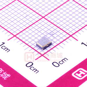
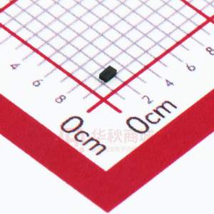
SG-3030LC SG-3040LC Actual size LC Type.
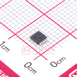
SG-3030JF
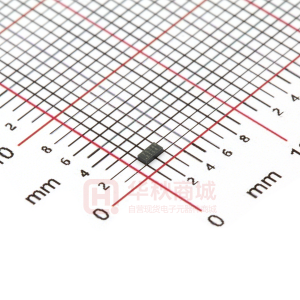
SG-3030JC SG-3040JC JC Type.
JF Type.
Specifications (characteristics)
Item Output frequency range Supply voltage Interface power supply voltage Storage temperature Temperature range Operating temperature Frequency tolerance Frequency temperature coefficient Frequency / voltage coefficient Current consumption Symmetry High output voltage Low output voltage Output load condition (CMOS) Symbol
f0
VCC VIO T_stg T_use f_tol fo-TC fo-VCC ICC SYM VOH VOL L_CMOS
+25 °C,VCC=3.3 V (SG-3040: VCC=1.2 V) -20 °C to +70 °C (+25 °C is reference) +25 °C 3.3 V, No load condition 1/2 VCC(VIO)level (SG-3040: VIO=1.2 V to 3.6 V) IOH=-0.4 mA (SG-3040: VIO=1.2 V to 3.6 V) IOL= 0.4 mA (SG-3040: VIO=1.2 V to 3.6 V) CMOS load CMOS load:20 % VCC(VIO) to 80 % VCC(VIO)level Rise time / Fall time tr / tf 200 ns Max. 100 ns Max. (SG-3040: VIO=1.2 V to 3.6 V) Time at minimum Supply voltage to be 0 s 1 s Max. 3 s Max. Start-up time t_str +25 °C (SG-3030: VCC= 2.0 V to 5.5 V) -6 Frequency aging f_aging ±5 × 10 / year Max. +25 °C, VCC= 3.3 V, First year Unless otherwise stated, characteristics (specifications) shown in the above table are based on the rated operating temperature and voltage condition.
Specifications SG-3030LC / JF / JC SG-3040LC / JC 32.768 kHz 1.5 V to 5.5 V 0.9 V to 3.6 V 1.5 V to 5.5 V 0.9 V to 3.6 V -55 °C to +125 °C -40 °C to +85 °C 5 ±23 × 10-6 +10 × 10-6 / -120 × 10-6 ±2 × 10⁻⁶ / V Max. ±5 × 10⁻⁶ / V Max. 2 μA Max. 3.1 μA Max. 45 % to 55 % VIO-0.4 V Min. 0.4 V Max. 15 pF Max.
Remarks
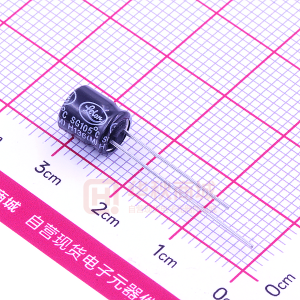
Store as bare product after unpacking
Block diagram
VCC V
I
V C OR E VO RD CD
V IO I f V IO f unction is not used, connect #1 to V C C . OUT
32.768 k Hz
RF CG GND
External dimension
S G-3030LC / 3 040LC
3 .6 ± 0.2
# 12 #7 P in map C onnection P in 1 V IO 2 N .C. 3 N .C. 4 N .C. 5 N .C. 6 G ND P in 12 11 10 9 8 7
C onnection
(Unit:mm)
S G-3030JF
7 .1 ± 0.2
V CC N.C. N.C. N.C. N.C. OUT #4 #3 P in map P in 1 2 3 4
Connection
S G-3030JC / 3040JC
#4 1 0.5 Max. #3 5.8 Max. 5.0
P in map P in 1 2 3 4 C onnection V IO G ND O UT V CC
A 123B
#1 #6
4.6±0.2 5.1±0.2
2.4
E 3040
S G3030 B E 9245A
#1 #2
V IO G ND O UT V CC
S G3030 B
E
#1
8 123A
#2
1.2 Max.
0.4 2 .8 ± 0.2
5 .08
0 Min.
(0.75)
(0.75)
2.7 Max.
0 .5
0.22
1.5 Max.
0.51
0 M in.
( 0.4 )
5.08 0.05Min.
(1.0) 3 .6
(1.0)
M etal may be exposed on the top or bottom of this product. This will not affect any quality, reliability or electrical spec.
Footprint (Recommended)
SG-3030LC / 3040LC
0.8 2.5
(Unit:mm)
SG-3030JF SG-3030JC / 3040JC
1.8 2.0 1.3 2.1 4.6 5.08 5.08
3.2
1.6
2.4
0.5
0.27
0.8
2.77
To maintain stable operation, provide by-pass capacitor with more than 0.1 μF at a location as near as possible to the power source terminal of the crystal products (between VCC - GND).
http://www.epsontoyocom.co.jp
4.2
�
很抱歉,暂时无法提供与“SG-3030LC_10”相匹配的价格&库存,您可以联系我们找货
免费人工找货- 国内价格
- 1+5.21611
- 10+4.544
- 100+3.87318
- 国内价格
- 10+0.23009
- 100+0.21014
- 500+0.19019
- 1000+0.17024
- 2000+0.15694
- 4000+0.15295
- 国内价格
- 10+0.22719
- 50+0.21015
- 200+0.19595
- 600+0.18175
- 1500+0.1704
- 3000+0.1633
- 国内价格
- 10+0.29561
- 100+0.23562
- 200+0.23209
- 400+0.22977
- 1000+0.22517
- 国内价格
- 10+0.27023
- 100+0.2468
- 500+0.22337
- 1000+0.19994
- 2000+0.18432
- 4000+0.17963
- 国内价格
- 1+1.05994
- 30+1.02209
- 100+0.98423
- 500+0.90852
- 1000+0.87066
- 2000+0.84795
- 国内价格
- 5+1.8328
- 50+1.43766
- 150+1.26832
- 国内价格
- 1+2.4651
- 10+1.9404
- 600+1.3167
- 1200+1.30353
- 3000+1.27746
- 国内价格
- 1+1.2183
- 30+1.1718
- 100+1.1253
- 500+1.0323
- 1000+0.9858
- 2000+0.9579