C8051F020 C8051F020
ANALOG PERIPHERALS
12-bit ADC ! ±1LSB INL ! Programmable Throughput up to 100ksps ! 8 External Inputs; Programmable as Single-Ended or Differential ! Programmable Amplifier Gain: 16, 8, 4, 2, 1, 0.5 ! Data Dependent Windowed Interrupt Generator ! Built-in Temperature Sensor (± 3°C) 8-bit ADC ! Programmable Throughput up to 500ksps ! 8 External Inputs ! Programmable Amplifier Gain: 4, 2, 1, 0.5 Two 12-bit DACs ! Can Synchronize Outputs to Timers for Jitter-Free Waveform Generation Two Comparators Internal Voltage Reference Precision VDD Monitor/Brown-out Detector On-Chip Debug Circuitry Facilitates Full Speed, Non-Intrusive InSystem Debug (No Emulator Required!) Provides Breakpoints, Single Stepping, Watchpoints, Stack Monitor Inspect/Modify Memory and Registers Superior Performance to Emulation Systems Using ICE-Chips, Target Pods, and Sockets IEEE1149.1 Compliant Boundary Scan Low Cost, Complete Development Kit: $129
Mixed-Signal 64KB ISP FLASH MCU
PRELIMINARY
HIGH SPEED 8051 µC CORE
Pipe-lined Instruction Architecture; Executes 70% of Instructions in 1 or 2 System Clocks Up to 25MIPS Throughput with 25MHz System Clock 22 Vectored Interrupt Sources 4352 Bytes Internal Data RAM (256 + 4k) 64k Bytes In-System Programmable FLASH Program Memory External Parallel Data Memory Interface – up to 5Mbytes/sec 64 Port I/O; All are 5V tolerant Hardware SMBusTM (I2CTM Compatible), SPITM, and Two UART Serial Ports Available Concurrently Programmable 16-bit Counter/Timer Array with 5 Capture/Compare Modules 5 General Purpose 16-bit Counter/Timers Dedicated Watch-Dog Timer; Bi-directional Reset Internal Programmable Oscillator: 2-to-16MHz External Oscillator: Crystal, RC, C, or Clock Real-Time Clock Mode using Timer 3 or PCA Typical Operating Current: 10mA @ 25MHz Multiple Power Saving Sleep and Shutdown Modes
MEMORY
-
DIGITAL PERIPHERALS
VDD VDD VDD DGND DGND DGND AV+ AV+ AGND AGND TCK TMS TDI TDO /RST
CLOCK SOURCES
ON-CHIP JTAG DEBUG & BOUNDRY SCAN
SUPPLY VOLTAGE ........................ 2.7V to 3.6V 100-Pin TQFP (64-Pin Version Available) Temperature Range: –40°C to +85°C
Port I/O Config.
Digital Power
Analog Power
JTAG Logic
Boundary Scan Debug HW
Reset
8 0 5 1 C o r e
UART0 UART1 SMBus SPI Bus PCA
P0 Drv
P0.0 P0.7
SFR Bus
64kbyte FLASH 256 byte RAM 4kbyte RAM
Timers 0, 1, 2, 4 Timer 3/ RTC P0, P1, P2, P3 Latches Crossbar Config.
ADC 500ksps (8-Bit)
MONEN
VDD Monitor External Oscillator Circuit Internal Oscillator
C R O S S B A R
P1 Drv
P1.0/AIN1.0 P1.7/AIN1.7
P2 Drv
P2.0 P2.7
WDT
P3 Drv
P3.0 P3.7
XTAL1 XTAL2
System Clock
VREF1
Prog Gain
VREF VREFD DAC1
VREF
A M U X
8:1
DAC1 (12-Bit) DAC0 (12-Bit)
External Data Memory Bus
Bus Control
P4.0
DAC0 VREF0 AIN0.0 AIN0.1 AIN0.2 AIN0.3 AIN0.4 AIN0.5 AIN0.6 AIN0.7 CP0+ CP0CP1+ CP1-
C T L
P4 Latch
P4 DRV
P4.4 P4.5/ALE P4.6/RD P4.7/WR P5.0/A0 P5.7/A7 P6.0/A8 P6.7/A15
A M U X
Prog Gain
ADC 100ksps (12-Bit)
Address Bus
A d d r
P5 Latch P6 Latch
P5 DRV P6 DRV
TEMP SENSOR
Data Bus
CP0
D a t a
P7 Latch
P7 DRV
P7.0/D0 P7.7/D7
CP1
7.26.2001
�C8051F020 C8051F020
Mixed-Signal 64KB ISP FLASH MCU
PRELIMINARY
SELECTED ELECTRICAL SPECIFICATIONS TA = -40°C to +85°C unless otherwise specified. PARAMETER CONDITIONS MIN TYP GLOBAL CHARACTERISTICS Digital Supply Voltage 2.7 10 Digital Supply Current with Clock=25MHz 0.8 CPU active (VDD=2.7V) Clock=1MHz 20 Clock=32kHz; VDD Monitor Disabled 10 Digital Supply Current Oscillator not running; VDD Monitor (shutdown) Enabled Oscillator not running; VDD Monitor 0.1 Disabled Digital Supply RAM Data 1.5 Retention Voltage CPU & DIGITAL I/O PORTS Clock Frequency Range DC Port Output High Voltage IOH = -3mA, Port I/O push-pull VDD – 0.7 Port Output Low Voltage IOL = 8.5mA Input High Voltage 0.7 x VDD Input Low Voltage A/D CONVERTER Resolution 12 Integral Nonlinearity Differential Nonlinearity Guaranteed Monotonic Signal-to-Noise Plus 66 Distortion Throughput Rate Input Voltage Range 0 COMPARATORS Response Time | CP+ – CP- | = 100mV 4 Input Voltage Range -0.25 Input Bias Current -5 0.001 Input Offset Voltage -10
MAX 3.6
UNITS V mA mA µA µA µA V
25 0.6 0.3 x VDD ±1 ±1
MHz V V V V bits LSB LSB dB ksps V µs V nA mV
100 VREF
VDD + 0.25 +5 +10
PACKAGE INFORMATION
D D1
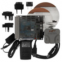
C8051F020DK DEVELOPMENT KIT ($129)
MIN NOM MAX (mm) (mm) (mm) A 1.20 0.15
A1 0.05
A2 0.95 1.00 1.05 b D
E1 E
0.17 0.22 0.27 16.00 14.00 0.50 16.00 14.00 -
D1 e E E1
100 PIN 1 DESIGNATOR 1
A2
e A b A1
SMBus is a trademark of Intel Corp.; I2C is a trademark of Philips Semiconductors, Inc.; SPI is a trademark of Motorola, Inc.
�
很抱歉,暂时无法提供与“C8051F020DK”相匹配的价格&库存,您可以联系我们找货
免费人工找货