DATA SHEET
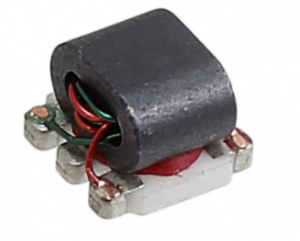
AC-PLM-1 Powerline Modem
DS01052 - January 2005 Revision March 2005
#$ %& ' ( ! ) $* +) ! " + " "* " )! $ , ! +* !" ., , ! !$ ! +$ * / ) $ !'( % %! ! * !$ +. !* ! , + )! + .) , "! ""! + ! $ +. + $* #$ " + " + ! "* , $) $., ! ) +) ! "* " $) $ * , "! * "" ! 0 #$ $ ! ! " $! ' ( % * ! "* $! * ! ! *
1' + " + ! 2 $3 $) $ "" $" ! ! !+ "+! % ) !""! ! +! ," 4 !+ 4 44 4 ! + 4 % ) !""! ! ! ,3 ,"5 4 5 40 7 46 "* &+" 8 & 9) $ +. $$! +! + ! + "* " + $$ ! ! + + '& * + !+ % ) !""! *0 * ! "! !) " $, . 8) $$ $) $ ! + +! + ! +, + 9 %0 3 ! ), : + 8; < 9 6) , $, 1 ! +: 89 1: :, , ++ ! ! + )+ + ) 1 !! * "! !) " ) !0 + +! + ) !0 + +" ) !) !" +, + ! " ), !" +* ! * 0 ! = %! ! !+ ! ,* ! 8% ' ( "* ! 9 % ! !* ! $) $.* *0 ! 8 0 +, + * 9! ) 0
!!
"
�#$ %& , , $* !*! "" ! . * * ! ++ ! + #$ * 0" * 0
+! ! + , , $ ) %&
$ #$ + ! , " $ ! ! . + "* .+ . !" * ) !+$ ! $ ! .+ $
%
"* ! "* $, ! +. ! 0 ! " ,"! ! " + ! + ! . 1 ! ,$ 3 +( , ! 0 0$
#$ ,$ % & * .+ ! , , "> + ! $ 0, 3 $ ! +! ! + $! ,3 ! " , * !" ! ! !+ ) #$ ! ! +* !" ! ! + , ) $ %& , !$ , $+ ! $ %& * .$ ! ), * !" ! .! "" ! * #$ 1 * +! $$ ! ,! ) )$ ! .+ $
' $! . ) $" ! ! ! +" + ! ! !" , ! ". $ , ! +, 3 ! ! * .+ $ "* !+ $ ! ,3 $ +) !"
)' ( "* ! % $ "" ! * ,$ %& ! 0+ ! " $ !* ! * 3 #$ !" "" ! *! ! % .! ""! +, " $ %& #$ , )! $ $ , ! ,$ "" ! ** !+ $ ! ,$ %; % * A ? #@ :
>
&% %
#$ ! %& $* *> $ ) + . " + " ! +! !* ! * !
"! & ; !+ )8 &; 9 ;" *! !+' + ) $+ ;" !) ' )& $ ) # "
! " %; ? #4 %; ?# %; ?# %; ?# %; ?# %; ? #5 %; ? #< %; ? #C % >' /@ %/ @ >' '( '? %2? % %2 $*'
(? 4% (? -> ' /@ (? - > ' %/ @ (? (? ; B ' #; $*'
)' $ $ B! ? #$ " !6 0 ' ! "' %* !
!!
"
2/7
�'
() *
The external circuit diagrams can be provided upon request.
&+ , -+# -
)*
!!
"
3/7
�&+ , -+# Pin Name
CK HCK 2 INT 2 HSK VDDCORE VSSOUT OSCI VDDOUT VSSCORE 1,2 PORT0 1,2 PORT1 1,2 PORT2 1,2 PORT3 1,2 PORT4 1,2 PORT5 PORT6 1,2 PORT7 2 POEN3 2 POEN4 PORTYPE 1,2 CSPOL RCVNG XING 2 IN 2 XOUT
2 1,2 1,2
)
Drive (mA)
1 1 2 2 2 2 2 2 2 2 2 8 8 1 1 1 1 1 1 1 1 1 1 1 1 1 * *
%
Type
Output Output Output Tri-state VCC GND Input VCC GND Inout Inout Inout Inout Inout Input Input Input Output Output Input Input Output Output Input Output Output Output Output Input Output Output Output Output Output Output Output Output Output Output Output
Pin No.
1 2 3 4 5,27 6,30 7 8,28 9,31 10 11 12 13 14 15 16 17 18 19 20 21 22 23 24 25 26 29 32 33 34 35 36 37 38 39 40 41 42 43 44
Functions
Frequency carrier = OSCI/XDVI. OSCI clock output. Interrupt. Handshake signal. 3.3V input. Ground signal. Input clock signal. 3.3V input. Ground signal. Data IO 0 / Data available on the communication port. Data IO 1 / Line busy indication. Data IO 2 / Communication port busy indication. Data IO 3 / Serial data in (SDI). Data IO 4 / Serial data out (SDO). Clock polarity in serial mode / read-write enable in parallel mode. Read = 1’b1. Strobe or clock signal. Chip Select. Port output enable for PORT3. Output when POEN3 = 1. Port output enable for PORT0, 1, 2 and 4. Output when POEN4 = 1. Communication port type. 1 = Parallel, 0 = serial. Chip Select polarity. 1 = CS active high. Receiving a valid packet. Can drive a LED. Active low. Transmitting a valid packet. Can drive a LED. Active low. Receiver input. Transmitter output. Need to be filtered to eliminate second frequency generated by the chip. Amplifier enable signal. Hardware reset. Active low. Internal pull-up. Configuration status. Active high. Can drive a LED. Use to internal test. Internal pull-down. Must be tied to GND. DEBUG pin. Receiver burst pulse. No connect. DEBUG pin. Receiver side. Start of packet pulse. No connect. DEBUG pin. Receiver side. End of field. No connect. DEBUG pin. Receiver side. End of packet. No connect. DEBUG pin. Receiver side. A bit of a packet. DEBUG pin. Receiver side. Strobe to validate a RBIT. DEBUG pin. Line busy indicator. DEBUG pin. TX side. Output bit before modulation. DEBUG pin. TX side. Output bit strobe. DEBUG pin. TX side. Command indicator. Use by BIST test. Internal pull-down. Must be tied to GND.
XOUTE RESET CNFGD 3 SCAN_EN RBURSTP RSOPP REOF REOP RBIT RBITSTR LBUSY XBITOUT XBITSTR XCMD TESTMODE
#$ * $ ! * "! ! #$ * 5# ! #$ * $ ! * "! !
* ,4 $ 52 " +
!!
"
4/7
�*) *
T7 PLM1_CS (PORT7) T2 PLM1_SCK (PORT6) T5 PLM1_MISO (PORT4)
MSB OUT LSB OUT
T1
T6
T4 T3 PLM1_MOSI (PORT3)
MSB IN LSB IN
Num 1 2 3 4 5 6 7
tcyc = 1/fOSCI
Function SCK period Enable Time Data Setup Time Data Hold Time Slave Access Time Enable Log Time Sequentiel Transfer Time
Min 4 4 30 30 2 2
Max 32
2
Unit tcyc tcyc ns ns tcyc tcyc tcyc
%
*
'* * !) '* * !) 0, 3 > + ! D ! + +$ , $ ! , E + ! ,3 ! ,3 ,$ !" , " # "* ! . 4 4 4 44 4 5 4 4 % . . < < 4 4 /
?: ; ?# /
?( ' 1( 1 #
!
< 5 < 5
!"
&6 7 07 6 07 6 G
54 4 F 5
!!
"
5/7
�%
(* ## # (* ## # ?* ?*
0
. % . !) 8 !) 8 !) !) ## ## 5 5 4 4 -. 4F /
(
(6
? ? 6
. !9 . !9 . 6) $.
&
-
*
4 FG 5 5 5 5 G FG F "B I F" 4&6 7
" * ! ) "* ! ' !) # "* ! H # "* ! % +* ! #$ "! " " &! " " ? ! )1 3 *
!
'* '
&+ , -+# -
,
!!
"
6/7
�&+ , -+# -
(* ) *
1
+2 " 2
*
0
"
%+ " A %& ! A ! E! !
0
B A !! "
# AJ 1! A J
FF C FF C
F
!!
"
7/7
�