Prepared Checked Approved
Product Specifications
Ref No. Total Page Page No.
A 17 1
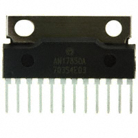
AN17850A
Structure Appearance Application Silicon Monolithic Bipolar IC SIL-12 Pins Plastic Package (FP-12S Power Type With Fin) Audio
Function
70W (6Ω) x 1ch BTL Power Amplifier Built-in Standby and Muting Features Incorporating Various Protection Circuits
A No. 1 2 3 4 5 6 7 8 Item
Storage Temperature
Absolute Maximum Ratings Symbol
Tstg Topr Popr Gopr Sopr Vcc Icc PD
Ratings
-55 ~ +150 -25 ~ +75
1.013x10⁵ ±0.61x10⁵
Unit
°C °C Pa m/s m/s V A W
2 2
Note
Operating Ambient Temperature Operating Ambient Pressure Operating Constant Acceleration Operating Shock Power Supply V oltage Power Supply Current Power Dissipation
9,810 4,900
33 8.0 37.5
1
2
Operating Supply V oltage Range
Vcc
10 V ~ 32V
Note: 1) Without input signal, Vcc is up to 33V 2) Ta = 75°C with infinite heatsink
Eff. Date
15-AUG-03
Eff. Date
Eff. Date
Eff. Date Semiconductor Company, Matsushita Electric Industrial Co., Ltd.
FMSC-PSDA-002-01 REV 1
�Prepared Checked Approved
Product Specifications
Ref No. Total Page Page No.
B-1 17 2
AN17850A
B
No. 1 2 3 4 5 6 7 8 9
Electrical Characteristics
Item
Quiescent Circuit Current Output Noise V oltage V oltage Gain Total Harmonic Distortion Maximum Output Power Output Offset V oltage Ripple Rejection Standby Current Muting Effects
(Unless otherwise specified, the ambient temperature is 25°C±2°C, Vcc=30V, frequency=1kHz and RL=6Ω.)
Test Symbol Circuit.
Icq Vno Gvc THD Po V off RR 1 1 1 1 1 1 1 1 1
Condition
No input ; Vstby = 5V Vmute = 5V;
No Input, Rg=20kΩ Vstby = 5V;Vmute = 5V
Limit Unit Note Min Typ Max
-
100 0.54 40 0.07 70 0 55 1 75
300 1 42 0.4
-
mA
mVrms
1
Vin=20mV; Vstdby=5V Vmute = 5V Vin=20mV; Vstdby=5V Vmute = 5V;
THD_OUT=10% Vstdby=5V;Vmute= 5V;
38
-
dB % W
mV
2
55 -350 45
-
Rg=20kΩ; No input Vstdby=5V;Vmute=5V; Vripple=1Vrms * freq=120Hz, Rg=20kΩ No input ; vstdby=0V; Vmute=5V; Vin=20mV; Vstby=5V; Vmute = 0 to 5V**
350
-
dB µA dB
1
I STB
MT
100
-
65
2
* The measurement is by taking the ratio of output voltage with reference to the Vripple.
** The measurement is by taking the ratio of output (at Vmute = 0 V) to the output(at Vmute = 5V)
Note : 1) With a filter band 20Hz ~20kHz (12 dB/OCT) used. 2) With a filter band 400Hz ~30kHz used.
Eff. Date
15-AUG-03
Eff. Date
Eff. Date
Eff. Date Semiconductor Company, Matsushita Electric Industrial Co., Ltd.
FMSC-PSDA-002-01 REV 1
�Prepared Checked Approved
Product Specifications
(Reference Data for Design)
Ref No. Total Page Page No.
B-2 17 3
AN17850A
B Electrical Characteristics
No Item 1 2 3 Standby on voltage Standby off voltage Mute on voltage
(Unless otherwise specified, the ambient temperature is 25°C±2°C, Vcc=30V, frequency=1kHz and RL=6Ω.)
Test Symbol Cir- Conditions cuit
Vstdon
Limits min typ max 4.5 4 1 1 -
Unit Note V V V V
1 1 1 1
Vmute = 5V; Vin = 20mV; Istb < 100uA Vmute = 5V; Vin = 20mV; Gvc > 38 dB
Vstd0ff Vmon Vmoff
VStdby = 5V; Vin = 20mV; MT > 70 dB VStdby = 5V; Vin = 20mV; Gvc > 38 dB
4 Mute off voltage
Note)
The above characteristics are reference values determined for IC design, but not guaranteed values for shipping inspection. If problems were to occur, counter measures will be sincerely discussed.
Eff. Date
15-AUG-03
Eff. Date
Eff. Date
Eff. Date Semiconductor Company, Matsushita Electric Industrial Co., Ltd.
FMSC-PSDA-002-01 REV 1
�Prepared Checked Approved
Product Specifications
Ref No. Total Page Page No.
C 17 4
AN17850A
(Description of Test Circuits and Test Methods)
Test Circuit 1
A
SW1 + 2200µ D Vcc=30V Vripp=1Vrms freq=120 Hz
33µF
8.2kΩ
6
4 NC MUTE
+
1 NC
12 VCC
OUT/+VE 10
SW4
B
A
+5V
1 NC 5 IN
AN17850A
OUT/-VE 7 STDBY NC PWRGND 9
RL= 6 Ω
AC, DC Voltmeter Distortion Meter Noise Meter
A
SW2
20k
INGND
3
+ 10µF
2
51k
8
OPEN
Vin
SW3
B
A
+5V
No. 1 2 3 4 5 6 7 8 9
Item ICQ Vno Gvc THD PO Voff R.R ISTB MT
SW1 OPEN Closed Closed Closed Closed Closed D OPEN Closed
SW2 SW3 OPEN A OPEN A A A A OPEN OPEN OPEN A A A A A A B A
SW4 A A A A A A A A B/A
Note : * STB 'OFF' means 5V . MUTE 'OFF' means 5V . Eff. Date
15-AUG-03
FMSC-PSDA-002-01 REV 1
Eff. Date
Eff. Date
Eff. Date Semiconductor Company, Matsushita Electric Industrial Co., Ltd.
�Prepared Checked Approved
Product Specifications
Ref No. Total Page Page No.
D 17 5
AN17850A
Circuit Function Block Diagram
Protection circuit Thermal Shutdown Load Short VCC Short Ground Short ASO Protection Over Voltage protection
REF + + -
AN17850A
-
+ MUTE
NC
STDBY
IN GND
NC
IN
MUTE
-VE OUT
NC
PWR GND
+VE OUT
NC
VCC
1
10µF
+
2
51kΩ
3
4
5
6
33µF+ 20kΩ 8.2kΩ
7
8
9
10
11
12
2200µ +
OFF/5V
OFF/5V
6Ω
ON/0V ON/0V
VCC
Pin Descriptions
Pin No. 1 2 3 4 5 6 Pin Descriptions NC STDBY IN GND NC IN MUTE Pin No. 7 8 9 10 11 12 Pin Descriptions -VE PHASE OUTPUT NC PWR GND +VE PHASE OUTPUT NC VCC
Eff. Date
15-AUG-03
Eff. Date
Eff. Date
Eff. Date Semiconductor Company, Matsushita Electric Industrial Co., Ltd.
FMSC-PSDA-002-01 REV 1
�Prepared Checked Approved
Product Specifications
Ref No. Total Page Page No.
E 17 6
AN17850A
Package Name Unit : mm
FP-12S
∅ 3.6
6.4 ± 0.3
7.7 ± 0.3
12
7.8 ± 0.3
29.96 ± 0.3
28.0 ± 0.3
20.0±0.1
0.6
R1.8
1
1.2 ± 0.1
+0.1 0.25 -0.05
2.54
0.6 ± 0.1
3.5 ± 0.3
Eff. Date
15-AUG-03
Eff. Date
Eff. Date
Eff. Date Semiconductor Company, Matsushita Electric Industrial Co., Ltd.
FMSC-PSDA-002-01 REV 1
29.6 ± 0.3
Name of item Date Code Company insignia
�Prepared Checked Approved
Product Specifications
Ref No. Total Page Page No.
F 17 7
AN17850A
SiN, Fe group, Ag plating, Solder plating, Ag paste, PSG, Cu group, Au plating, Solder dip, Au-Si alloy,
(Structure Description)
Chip surface passivation Lead frame material Inner lead surface process Outer lead surface process Chip mounting method Wire bonding method Wire material Mold material Molding method Fin material Others ( Others ( Others ( Others ( Solder, Others ( Others ( Others ( Others ( Multiplunger mold, Others ( Others ( ) ) ) ) ) ) ) ) ) )
1 2, 6 2 6 3 4 4 5 5 7
Thermalsonic bonding, Au Epoxy, Transfer mold, Cu Group
Package FP-12S
1 4 3
5
6
7
2
Eff. Date
15-AUG-03
Eff. Date
Eff. Date
Eff. Date Semiconductor Company, Matsushita Electric Industrial Co., Ltd.
FMSC-PSDA-002-01 REV 1
�Prepared Checked Approved
Product Specifications
(Technical Data)
Ref No. Total Page Page No.
G-1 17 8
AN17850A
Application Circuit
VCC= 30V NC
4 12
VCC
2200µ
IN GND
3
1
NC Output GND NC
AN17850A
51kΩ
9
STB
10µF
2
STB Vref MUTE
8
8.2kΩ
MUTE
33µF
6
OUT +ve
34dB
10 11 NC
IN
20kΩ
5
34dB
RL=6Ω
7
OUT -ve
STB 'OFF' STB 'ON' Mute 'OFF' Mute 'ON' Eff. Date
15-AUG-03
FMSC-PSDA-002-01 REV 1
5V 0V 5V 0V Eff. Date Eff. Date Semiconductor Company, Matsushita Electric Industrial Co., Ltd.
Eff. Date
�Prepared Checked Approved
Product Specifications
(Technical Data)
Ref No. Total Page Page No.
G-2 17 9
AN17850A
(1) Tc = Ta, 62.5W ( θj-c = 2 °C/W ) (2) 20.83W ( θf = 4.0 °C/W )
PD - Ta Curves
With a 100cm2 X 3mm Al heat sink (black colour coated) or a 200cm2 X 2mm Al heat sink (not lacquered) (3) 15.63W ( θf = 6.0 °C/W ) With a 100cm X 2mm Al heat sink (not lacquered) (4) 3.0W at Ta = 25°C ( θj-a = 42°C/W ) Without heat sink
2
80
70
62.5W
60 Power Dissipation PD ( W )
(1)
50
40
30
20.8W (2) 15.6W (3)
20 10
3.0W
(4)
0 0 25 50 75 100 125 150
Ambient Temperature Ta ( °C )
Eff. Date
15-AUG-03
Eff. Date
Eff. Date
Eff. Date Semiconductor Company, Matsushita Electric Industrial Co., Ltd.
FMSC-PSDA-002-01 REV 1
�Prepared Checked Approved
Product Specifications
(Technical Data)
Ref No. Total Page Page No.
G-3 17 10
AN17850A
Area of Safe Operation
40 VCEmax = 32V ICmax = 8A Ta = 25°C
10 8
t= s 1m
IC(A)
t= 10 s m s 0m t= 10
1
0.3 1 10 70
VCE (V)
Eff. Date
15-AUG-03
Eff. Date
Eff. Date
Eff. Date Semiconductor Company, Matsushita Electric Industrial Co., Ltd.
FMSC-PSDA-002-01 REV 1
�Prepared Checked Approved
Product Specifications
(Technical Data)
Ref No. Total Page Page No.
G-4 17 11
AN17850A
ta td
VCC = 30V
tb
VCC = 0V
tc
STANDBY OFF STANDBY ON
5V 0V 5V 0V
MUTE OFF MUTE ON
Description
ta tb tc td
Wating time required for Standby to turn off after VCC is on. Wating time required for Mute turn off after Standby is off. Wating time required for Standby to turn on after Mute is on Waiting time required for VCC to turn off after Standby is on
Minimum
0 500 300 0
Unit
ms ms ms ms
Eff. Date
15-AUG-03
Eff. Date
Eff. Date
Eff. Date Semiconductor Company, Matsushita Electric Industrial Co., Ltd.
FMSC-PSDA-002-01 REV 1
�Prepared Checked Approved
Pin No.
Product Specifications
(Technical Data)
Ref No. Total Page Page No.
G-5 17 12
DC BIAS (V)
AN17850A
Internal circuitry
Function NC Standby
12
Description
1 2
Standby control pin Determined by external
400
2
Standby “ON” = 0V Standby “OFF” = 5V
100kΩ 100kΩ 10kΩ
3
3 4 5
IN GND NC INPUT
200Ω
5
Input ground
0V
400Ω
AC input Terminal
0V
33kΩ
3
8.3kΩ
6
MUTE
12 6
400Ω 10.6kΩ
MUTE Control
MUTE “OFF” = 5V MUTE ON = 0V
Determined
by external
30kΩ
2.65kΩ 3
575Ω
Eff. Date
15-AUG-03
Eff. Date
Eff. Date
Eff. Date Semiconductor Company, Matsushita Electric Industrial Co., Ltd.
FMSC-PSDA-002-01 REV 1
�Prepared Checked Approved
Pin No.
Product Specifications
(Technical Data)
Ref No. Total Page Page No.
G-5 17 13
DC BIAS (V)
AN17850A
Internal circuitry
12
Function Output (-)
Description
Negative output terminal
7
VCC/2
Pre Amp
VCC/2 250Ω
Driver cct 7
15kΩ
9
10kΩ 3
8 9
NC PWR GND Output Power Ground
12
0V VCC/2
10 Output (+)
Pre Amp
VCC/2 250Ω 15kΩ 9 Driver cct 10
Positive output terminal
10kΩ 3
11 12
NC VCC
Power Supply Pin
Typ 30V
Eff. Date
15-AUG-03
Eff. Date
Eff. Date
Eff. Date Semiconductor Company, Matsushita Electric Industrial Co., Ltd.
FMSC-PSDA-002-01 REV 1
�Prepared Checked Approved
Product Specifications
(Technical Data)
Ref No. Total Page Page No.
G-6 17 14
AN17850A
TA
HEAT SINK
Power dissipation and Heat Sink
TC
CASE
TJ
DIE
Definition of terms
θCA
θJC
FIG1. Simplified Illustration of IC PD: Power Dissipation and Heat Sink attached Tj: Junction Temperature TC: Case Temperature TA: Ambient Temperature θJC: Thermal Resistance of junction to case θCA: Thermal Resistance of case to ambient, normally through heat sink
The following two equations represent the relations of these terms. ( Tj - TC ) / θJC = PD (1) ( TC - TA ) / θCA = PD’ (2) For reliable and long-term, continuous operation, junction temperature should not exceed 125OC and θJC for FP-12S package is 2OC/W. Substitute these values in Equation 1. After specify the PD, TC can be determined. Assume no heat loss at the casing,i.e. all power is dissipated to the ambient through heat sink, which is quite true. So PD = PD’. Since TC is also known, one can determine the following using equation2: a) The rating of heat sink for specific maximum operating ambient temperature, or b) The maximum operating ambient temperature for specific heat sink rating. A more general equation can be used for rough calculation. ( TJ - TA ) / θJA = PD θJA = θCA + θJC (3) (4)
In this case, θJA is total thermal resistance of the heat sink and IC package. Therefore, for specified power dissipation, either heat sink rating or maximum operating ambient temperature can be decided if the other is known. Take note that it’s essential to know PD value before hand in order to work out other quantities. PD calculation is as shown. PD = Vcc x Icc - Po_total Vcc: DC supply voltage Icc: RMS value of IC current Po_total: Total output power
Eff. Date
15-AUG-03
FMSC-PSDA-002-01 REV 1
(5)
Eff. Date
Eff. Date
Eff. Date Semiconductor Company, Matsushita Electric Industrial Co., Ltd.
�Prepared Checked Approved
Product Specifications
(Technical Data)
Ref No. Total Page Page No.
G-6 17 15
AN17850A
Input DC biasing
5 20kΩ
Vin
Input DC bias is maintained at ground level. If the input signal contains DC bias voltage, AC coupling should be included on the application circuit. The value of 20kΩ resistor is set in order to achieve the minimum output DC offset.
FIG2. Input DC Biasing
Output Zobel Network
It should be noted that this device is designed such that the Zobel network (RC pair) at the output pins is not necessary for stable operation. In practical application, the Zobel network may be applied optionally for two reasons: a) Ensuring stability for different PCB layout and speaker types. b) Ability to withstand to high ESD levels.
FIG3. Output Zobel Network
10 7
Eff. Date
15-AUG-03
Eff. Date
Eff. Date
Eff. Date Semiconductor Company, Matsushita Electric Industrial Co., Ltd.
FMSC-PSDA-002-01 REV 1
�Prepared Checked Approved
Product Specifications
(Technical Data)
Ref No. Total Page Page No.
G-6 17 16
AN17850A
Standby operation
51kΩ
5
STB
10µF
Standby pin should be connected with carefully selected components in order to avoid “Pop Noise” during Standby ON/OFF transient. The 51k resistor and 10uF capacitor pair can delay the rising of voltage at pin 5 to reach the Standby threshold. When Standby is switching on together with supply, this delay would be very useful to ensure no “Pop Noise”.
FIG4. Standby Application circuit
If the Standby voltage is provided by a microcontroller, the suppression of “Pop” could even be better. For further details of timing and delay for standby circuit, please refer to page 11.
Mute operation
Mute pin should be connected with carefully selected components in order to avoid “Pop Noise” during MUTE ON/OFF transient. The 8.2k resistor and 33uF capacitor pair can delay the rising of voltage at pin 6 to reach the Mute threshold. When Mute is switching on together with supply, this delay would be very useful to ensure no “Pop Noise”. 8.2kΩ
6
Mute
33µF
FIG5. Mute application circuit
For further details of timing and delay for Mute application circuit, please refer to page 11.
Eff. Date
15-AUG-03
Eff. Date
Eff. Date
Eff. Date Semiconductor Company, Matsushita Electric Industrial Co., Ltd.
FMSC-PSDA-002-01 REV 1
�Prepared Checked Approved
Product Specifications
Ref No. Total Page Page No.
H 17 17
AN17850A
(Precaution for use)
1) Ground the radiation fin so that there will be no difference in electric potential between the radiation fin and ground. 2) The thermal protection circuit operates at Tj at approximately 150 C. Thermal protection circuit is reset automatically when the temperature drops. 3) Be sure to attach heatsink to the IC before use. Make sure that the heatsink is secured to the chassis. 4) In order to prevent IC from being damaged during the fault test, prior to standby switching from on to off or vice versa, it is important to assert the mute on. Please refer to the timing diagram on page 11.
Eff. Date
15-AUG-03
Eff. Date
Eff. Date
Eff. Date Semiconductor Company, Matsushita Electric Industrial Co., Ltd.
FMSC-PSDA-002-01 REV 1
�


 工商网监
湘ICP备2023018690号
工商网监
湘ICP备2023018690号
