BBA-322-A BBA-519-A
WIRELESS MADE SIMPLE ®
BBA SERIES RF AMPLIFIER DATA GUIDE
DESCRIPTION
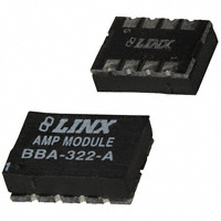
The BBA Series is a family of low-cost highperformance broadband RF amplifiers. The modules are ideally suited to a wide range of 0.360" AMP MODULE BBA-519-A amplification and buffering applications, LOT 0100 including extending the range of Linx’s own RF modules (where legally appropriate). Housed in 0.500" a compact SMD package, the hybrid amps are matched to 50Ω source and load impedances. The modules utilize a GaHBT gain stage, which 0.130" yields high gain and IP3, excellent flatness, and low noise. The BBA-322-A is the high gain Typ. model and is suitable for the LNA stage of many receivers. This extra gain stage on the front end of a receiver can improve the sensitivity and Figure 1: BBA Package Dimensions provide a greater range for the product. The BBA-519-A is the high power model and is suitable for the final gain stage in a transmitter. This amplifier can boost the output power of a transmitter to much higher levels and provide a significant increase in range (where legally appropriate).
BBA SERIES FEATURES
Prematched for 50Ω impedance No external RF components required Exceptional gain flatness Compact SMD package Operates from a single supply
BBA-322-A FEATURES
High gain 3.8dB noise figure DC-3GHz broadband operation +20dB small signal gain at 900MHz Up to +10dB (10mW) linear output power
BBA-519-A FEATURES
High output 4.8dB noise figure 10MHz-3GHz broadband operation +18dB small signal gain at 900MHz Up to +17dB (50mW) linear output power
APPLICATIONS INCLUDE
TX / RX Range Enhancement IF or RF Buffering Driver or Final Stage for PA General Purpose Gain Blocks
ORDERING INFORMATION
PART # DESCRIPTION BBA-322-A High Gain RF Amplifier BBA-519-A High Power RF Amplifier Amplifiers are supplied in tubes of 50 pcs.
Revised 1/28/08
�BBA-322-A ELECTRICAL SPECIFICATIONS
Parameter POWER SUPPLY Operating Voltage Supply Current AMPLIFIER SECTION Frequency Range Gain: @ 100MHz @ 1,000MHz @ 2,000MHz @ 3,000MHz Gain Ripple Noise Figure Input VSWR Output VSWR Output IP3 Output P1dB Reverse Isolation ANTENNA PORT RF Input Impedance ENVIRONMENTAL Operating Temperature Range – -40 – +85 RIN – 50 – Ω – – – – – – – – – FC – DC -50 – – – – – – – – – – – – – 21.0 20.0 17.0 14.0 ±2 3.8 2.3 2.1 +22.5 +11.2 20 3,000 +50 – – – – – – – – – – – MHz kHz dB dB dB dB dB dB – – dBm dBm dB 2 – – – – – 3 4 5 5 6 4 4 Designation VCC ICC Min. 4.8 – Typical – 35.0 Max. 5.2 65.0 Units VDC mA Notes 1 –
BBA-519-A ELECTRICAL SPECIFICATIONS
Parameter POWER SUPPLY Operating Voltage Supply Current AMPLIFIER SECTION Frequency Range Gain: @ 100MHz @ 1,000MHz @ 2,000MHz @ 3,000MHz @ 4,000MHz Gain Ripple Noise Figure Input VSWR Output VSWR Output IP3 Output P1dB Reverse Isolation ANTENNA PORT RF Input Impedance RIN – – -40 50 – – +85 Ω – – ENVIRONMENTAL Operating Temperature Range – – – – – – – FC – 10 -50 – – – – – – – – – – – – – – 18.5 17.5 15.5 13.5 12.5 ±2 4.8 2.1 1.8 +33 +18.5 20 4,000 +50 – – – – – – – – – – – – MHz kHz dB dB dB dB dB dB dB – – dBm dBm dB 2 – – – – – – 3 4 5 5 6 7 4 Designation VCC ICC Min. 4.8 – Typical – 60.0 Max. 5.2 65.0 Units VDC mA Notes 1 –
°C
Notes
1. 2. 3. 4. 5. 6. 5.2V to 12V range is possible with the appropriate current-limiting resistor. T = 25°C, ICC = 35mA. 100MHz to 2,000MHz. At 2,000MHz. In a 50Ω system, DC to 3,000MHz. At 2,000MHz ± 50kHz, PTONE = -18dBm.
°C
Notes
1. 2. 3. 4. 5. 6. 7. 5.2V to 12V range is possible with the appropriate current-limiting resistor. T = 25°C, ICC = 65mA. 100MHz to 2,000MHz. At 2,000MHz. In a 50Ω system, DC to 4,000MHz. At 1,000MHz ± 50kHz, PTONE = -10dBm. At 1,000MHz.
ABSOLUTE MAXIMUM RATINGS
Supply Voltage VCC Supply Current RF Input Operating Temperature Storage Temperature Soldering Temperature +4.8 to +5.2 65 +15 0 to +70 -60 to +150 +225°C for 10 seconds VDC mA dBm °C °C
ABSOLUTE MAXIMUM RATINGS
Supply Voltage VCC Supply Current RF Input Operating Temperature Storage Temperature Soldering Temperature +4.8 to +5.2 120 +13 0 to +70 -60 to +150 +225°C for 10 seconds VDC mA dBm °C °C
*NOTE* Exceeding any of the limits of this section may lead to permanent damage to the device. Furthermore, extended operation at these maximum ratings may reduce the life of this device.
*NOTE* Exceeding any of the limits of this section may lead to permanent damage to the device. Furthermore, extended operation at these maximum ratings may reduce the life of this device.
*CAUTION*
This product incorporates numerous static-sensitive components. Always wear an ESD wrist strap and observe proper ESD handling procedures when working with this device. Failure to observe this precaution may result in module damage or failure.
Page 2
*NOTE* The purchaser of this device should be aware that approvals may be required by applicable governing bodies for systems producing RF energy. It is the responsibility of the user to determine and adhere to the appropriate regulations for the region in which operation is intended.
Page 3
�PERFORMANCE DATA
These performance parameters are based on module operation at 25°C from a 5.0VDC supply with a -50dBm input unless otherwise noted. Figure 2 illustrates the connections necessary for testing and operation. It is recommended all ground pins be connected to the ground plane.
VCC 1 2 3 4 G ND GND RF OUT VCC GND GND GND RF IN GND BBA-519-A GND 8 7 6 5
THEORY OF OPERATION
The BBA Series is a family of low-cost, high-performance, broadband RF amplifiers. They utilize an advanced Gallium Arsenide Heterojunction Bipolar Transistor (HBT) gain stage, which yields high gain and IP3, excellent flatness, and low noise. They are self-contained with 50Ω input and output impedances and require only one external DC biasing resistor to operate as specified. The BBA-322-A is the high gain model and is suitable for the LNA stage of many receivers. This extra gain stage on the front end of a receiver can improve the sensitivity and provide a greater range for the product. The BBA-519-A is the high power model and is suitable for the final gain stage in a transmitter. This amplifier can boost the output power of a transmitter to much higher levels and provide a significant increase in range (where legally appropriate).
VCC
Figure 2: Test / Basic Application Circuit
PIN ASSIGNMENTS
1 2 3 4 GND RF OUT VCC GND GND GND RF IN GND 8 7 6 5
RF OUT
Figure 3: BBA Series Amplifier Pinout (Top View)
PIN DESCRIPTIONS Pin #
1 2 3 4 5 6 7 8
RF IN
Name
GND VCC GND RF IN GND GND GND RF OUT
Description
Analog Ground Supply Voltage Analog Ground 50-ohm RF Input
GND
Analog Ground
Figure 4: BBA Series Amplifier Schematic
Analog Ground Analog Ground 50-ohm RF Output
OPERATIONAL CONSIDERATIONS
The use of a gain stage can produce a significant increase in the range performance of an RF link. It is important to note that it can also introduce detrimental effects, such as the following: • Amplification of harmonics and LO along with the fundamental carrier frequency. • Adverse effect on the front-end noise figure on receivers. • Potential damage if the receiver input is not capable of accommodating high input power levels. • Risk of generating illegal power levels and unacceptable interference. It is up to the designer to ensure that the final product will comply with all appropriate regulations in the county of intended use.
Table 1: BBA Series Amplifier Pin Descriptions
Page 4
Page 5
�POWER SUPPLY REQUIREMENTS
The module does not have an internal voltage Vcc TO regulator; therefore it requires a clean, well-regulated MODULE power source. While it is preferable to power the unit 10Ω from a battery, the unit can also be operated from a Vcc IN power supply as long as noise is less than 20mV. 10μF Power supply noise can significantly affect the performance; therefore, providing a clean power supply for the module should be a high priority during Figure 5: Supply Filter design. A 10Ω resistor in series with the supply followed by a 10µF tantalum capacitor from VCC to ground will help in cases where the quality of supply power is poor. These values may need to be adjusted depending on the noise present on the supply line. The power supply must be regulated to within the primary range specified or the maximum current limited using an appropriate resistance in series with the amplifier’s positive supply pin. Failure to observe the supply limits will irreparably damage the device. The resistor should be selected so that the device current is limited to or less than the maximum rated current. The resistor value may be easily selected using the following formula:
+
TYPICAL APPLICATIONS
The schematic in the figure below shows a typical configuration for amplifying the output of a transmitter.
VCC VCC 1 GND RF OUT GND GND GND RF IN GND BBA-519-A GND 8 7 6 5
270Ω
1
TX DATA
GND
ANT GND 3 VCC LO V D 4 GND /CLK SE /CLK TXM-xxx-ES
PDN
10 9 8 7 GND 6
4
Figure 6: Typical Application Circuit
In this circuit, the BBA-519-A amplifies the output of the ES Series transmitter. The transmitter operates on 3V while the amplifier requires 5V, so a 270Ω resistor is used to drop the 5V supply to 3V for the transmitter. This configuration would result in a 6 to 7 times increase in system range. Note that such output levels may render the transmitter illegal for operation in certain countries, so it is up to the designer to ensure that the product will comply with the appropriate regulations.
R=
VSUPPLY - VDEVICE TYP. ICC 9-5 60x10-3 9-5 60x10-3 4 0.06
Example: BBA-519-A @ 9V Supply
R=
=
=
= 66Ω
Page 6
Page 7
�BOARD LAYOUT GUIDELINES
If you are at all familiar with RF devices, you may be concerned about specialized board layout requirements. Fortunately, because of the care taken by Linx in designing the modules, integrating them is very straightforward. Despite this ease of application, it is still necessary to maintain respect for the RF stage and exercise appropriate care in layout and application in order to maximize performance and ensure reliable operation. The antenna can also be influenced by layout choices. Please review this data guide in its entirety prior to beginning your design. By adhering to good layout principles and observing some basic design rules, you will be on the path to RF success. The adjacent figure shows the suggested PCB footprint for the module. The actual pad dimensions are shown in the Pad Layout section of this manual. A ground plane (as large as possible) should be placed on a lower layer of your PC board opposite the module. This ground plane can also be critical to the performance of your antenna, which will be discussed later. There should not be any ground or traces under the module on the same layer as the module, just bare PCB.
MICROSTRIP DETAILS
A transmission line is a medium whereby RF energy is transferred from one place to another with minimal loss. This is a critical factor, especially in highfrequency products like Linx RF modules, because the trace leading to the module’s antenna can effectively contribute to the length of the antenna, changing its resonant bandwidth. In order to minimize loss and detuning, some form of transmission line between the antenna and the module should be used, unless the antenna can be placed very close (