Preliminary
Product Specification
Features
-
Amp’ed RF, Inc.
(phone) 408 213-9530 (fax) 408 213-9533
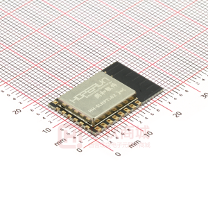
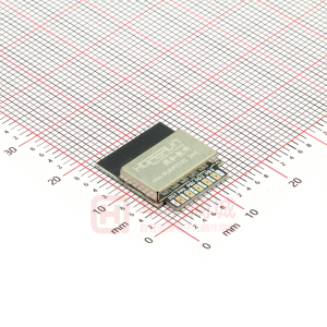
15mm x 27mm
Description
The added class 1 power, +16dBm, of the BT-11, gives this module one of the best ranges in the industry. It’s completely pin compatible with the lower power BT-21, and offers a second power choice on the same design. The BT-11 module includes 16 general purpose input/output lines, several serial interface options, analog-to-digital inputs, and up to 2M bps data throughput. The BT-11 is a surface mount PCB module that provides fully embedded, ready to use Bluetooth wireless technology. The reprogrammable flash memory contains embedded firmware for serial cable replacement using the Bluetooth SPP profile. Other popular Bluetooth profiles, such as OBEX, are also available. Customized firmware for peripheral device interaction, power optimization, security, and other proprietary features may be supported and can be ordered pre-loaded and configured.
-
Additional Documentation
BT Hardware Design Guide abSerial User Guide abSerial Reference Guide
Bluetooth Radio Fully embedded Bluetooth v2.1+EDR with profiles Class 1 radio Complete RF ready module Wireless data communications Integrated chip antenna 128-bit encryption security Range up to 120m LOS FCC & Bluetooth qualified Integrated antenna or with coaxial external connector ST Micro Cortex-M3 microprocessor up to 70MHz Memory 256K bytes flash memory 48K bytes RAM memory Data Rate 2M bps maximum data rate Multipoint capability up to 7 slaves Serial Interface UART, up to 3.25M bps SPI interface I2C interface USB v2.0 General I/O 16 general purpose I/O 4x12-bit A/D inputs 1 DAC output User Interface AT command set Firmware upgrade over UART
BT-11 Datasheet Page 1 of 12
©2008 Amp’ed RF Inc 1 10/07/08
1722 Ringwood Ave, Suite 250, San Jose, CA 95131, USA www.ampedrf.com
�Preliminary
Software Architecture
Lower Layer Stack
Full Bluetooth v2.1+EDR data rate (3M bps maximum) Device power modes—active, sleep and deep sleep Wake on Bluetooth feature—optimized power consumption of host CPU Authentication and encryption Encryption key length from 8-bits to 128-bits maximum Persistent FLASH memory—for BD Address and radio parameter storage All ACL (Asynchronous Connection Less) packet types (DM1, DH1, DM3, DH3, DM5, DH5, 2-DH1, 2-DH3, 2-DH5, 3-DH1 3-DH3, 3-DH5, AUX1) SCO (Synchronous Connection Oriented) packet types (HV1, HV2, HV3) Point to multipoint and scatternet support—3 master and 7 slave links allowed (10 active links simultaneously) Park, sniff, and hold modes—fully supported to maximum allowed intervals Master slave switch—supported during connection and post connection Dedicated Inquiry Access Code—for improved inquiry scan performance Dynamic packet selection—channel quality driven data rate to optimize link performance Dynamic power control—interference reduction and link performance Bluetooth test modes—per Bluetooth specification 802.11b co-existence—AWMA and AFH Vendor specific HCI commands—to support device configuration and certification test modes
Amp’ed RF, Inc.
(phone) 408 213-9530 (fax) 408 213-9533
Upper Layer Stack: Amp’ed UP
SPP, OBEX, SDAP, GAP, and DUN protocols RFComm, SDP, and L2CAP supported Multipoint with 7 simultaneous slaves
HCI Interface
Bluetooth v2.1 specification compliant HCI UART transport layer (H4)
UI Application BT profiles
SPP, OBEX, DUN, GAP HCI (over UART)
AT Commands Custom Applications
SDP
RFComm L2CAP HCI
Upper layer stack + BT profiles: Amp’ed UP!
HCI LMP BT PHY
Low-level BT stack embedded in Bluetooth IC
©2008 Amp’ed RF Inc 2 10/07/08
1722 Ringwood Ave, Suite 250, San Jose, CA 95131, USA www.ampedrf.com
BT-11 Datasheet Page 2 of 12
�Preliminary
Hardware Specifications
General Conditions (VIN= 3.0V and 25°C)
Amp’ed RF, Inc.
(phone) 408 213-9530 (fax) 408 213-9533
Recommended Operating Conditions
Rating Operating Temperature Range Supply Voltage VIN Signal Pin Voltage RF Frequency Min -30 2.7 2400 Typical 3.0 3.0 Max 80 3.6 2483.5 Unit °C Volts Volts MHz
Absolute Maximum Ratings
Rating Storage temperature range Supply voltage, VIN I/O pin voltage, VIO RF input power Min -55 -0.3 -0.3 Typical Max +150 + 3.6 + 4.0 -5 Unit °C Volts Volts dBm
Current Consumption
Modes Typical Power Consumption ACL data 115K Baud UART at max throughput (Master) ACL data 115K Baud UART at max throughput (Slave) Connection, no data traffic, master Connection, no data traffic, slave Connection in sniff (Tsniff=100ms), no data traffic, master Connection in sniff (Tsniff=100ms), no data traffic, slave Connection in sniff (Tsniff=375ms), no data traffic, master Connection in sniff (Tsniff=375ms), no data traffic, slave Standby, without deep sleep Standby, with deep sleep Page/Inquiry scan, deep sleep Avg 58.0 55.0 26.0 34.0 12.0 12.4 3.0 3.5 21.0 0.240 2.4 Unit mA mA mA mA mA mA mA mA mA mA mA
©2008 Amp’ed RF Inc 3 10/07/08
1722 Ringwood Ave, Suite 250, San Jose, CA 95131, USA www.ampedrf.com
BT-11 Datasheet Page 3 of 12
�Preliminary
Amp’ed RF, Inc.
(phone) 408 213-9530 (fax) 408 213-9533
I/O Operating Characteristics
Symbol VIL VIH VOL VOH IOL IOH RPU RPD
Parameter Low-Level Input Voltage High-Level Input Voltage Low-Level Output Voltage High-Level Output Voltage Low -Level Output Current High-Level Output Current Pull-up Resistor Pull-down Resistor
Min 2.1 2.2 50 50
Max 0.9 0.4 8.0 8.0 150 150
Unit Volts Volts Volts Volts mA mA KΩ KΩ
Conditions VIN, 3.0V VIN, 3.0V VIN, 3.0V VIN, 3.0V VOL = 0.4 V VOH = 2.2 V Resistor Turned On Resistor Turned On
Selected RF Characteristics
Parameters Antenna load Radio Receiver Sensitivity level Maximum usable level Input VSWR Radio Transmitter Maximum output power Initial Carrier Frequency Tolerance 20 dB Bandwidth for modulated carrier
Conditions
BT Spec
Typical 50
Unit ohm dBm dBm
BER < .001 with DH5 BER < .001 with DH1
≤ -70 ≥ -20
-90 -9 2.5:1
50 Ω load