TRM-315-LT TRM-418-LT TRM-433-LT
WIRELESS MADE SIMPLE ®
LT SERIES TRANSCEIVER MODULE DATA GUIDE
DESCRIPTION
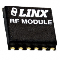
The LT Series transceiver is ideal for the bi0.619" directional wireless transfer of serial data, control, or command information in the favorable 260-470MHz band. The transceiver is capable of generating +10dBm into a 50-ohm load and achieves an 0.630" RF MODULE TRM-433-LT outstanding typical sensitivity of -112dBm. Its LOT 10000 advanced synthesized architecture delivers outstanding stability and frequency accuracy, and minimizes the effects of antenna pulling. When paired, the transceivers form a reliable wireless link 0.125" that is capable of transferring data at rates of up to 10,000bps over distances of up to 3,000 feet. Applications operating over shorter distances or at Figure 1: Package Dimensions lower data rates will also benefit from increased link reliability and superior noise immunity. Housed in a tiny reflow-compatible SMD package, the transceiver requires no external RF components (except an antenna), which greatly simplifies integration and lowers assembly costs.
FEATURES
Long range Low cost PLL-synthesized architecture Direct serial interface Data rates to 10,000bps No external RF components required Low power consumption Compact surface-mount package Wide temperature range RSSI and power-down functions No production tuning Easy to use
APPLICATIONS INCLUDE
2-Way Remote Control Keyless Entry Garage / Gate Openers Lighting Control Medical Monitoring / Call Systems Remote Industrial Monitoring Periodic Data Transfer Home / Industrial Automation Fire / Security Alarms / Access Control Remote Status / Position Sensing Long-Range RFID Wire Elimination
ORDERING INFORMATION
PART # DESCRIPTION TRM-315-LT Transceiver 315MHz TRM-418-LT Transceiver 418MHz TRM-433-LT Transceiver 433MHz EVAL-***-LT Basic Evaluation Kit *** = Frequency Transceivers are supplied in tubes of 33 pcs.
Revised 2/28/08
�ELECTRICAL SPECIFICATIONS
Parameter POWER SUPPLY Operating Voltage Supply Current Transmit Mode Logic High Transmit Mode Logic High Transmit Mode Logic Low Receive Mode Power Down Current DATA Line: Output Low Voltage Output High Voltage Input Low Threshold Input High Threshold Power Down Input: Input Low Threshold Input High Threshold RF SECTION Frequency Range: TRM-315-LT TRM-418-LT TRM-433-LT Center Frequency Accuracy Data Rate RECEIVER SECTION LO Feedthrough IF Frequency Noise Bandwidth Receiver Sensitivity RSSI / Analog: Dynamic Range Analog Bandwidth Gain Voltage with No Carrier TRANSMITTER SECTION Output Power With a 750Ω resistor on LADJ Output Power Control Range Harmonic Emissions ANTENNA PORT RF Input Impedance TIMING Receiver Turn-On Time: Via VCC Via PDN Max. Time Between Transitions Transmitter Turn-On Time: Via VCC Via PDN Modulation Delay Transmit to Receive Switch Time Receive to Transmit Switch Time Dwell Time ENVIRONMENTAL Operating Temperature Range Page 2 Designation VCC ICC Min. 2.1 – – – – – – – – 0.9VCC – 0.9VCC Typical 3.0 12 7.6 4.0 6.1 11.5 0.15 VCC-0.26 – – – – Max. 3.6 14 9.5 5.0 7.9 20.0 – – 0.1VCC – 0.1VCC – Units VDC mA mA mA mA µA VDC VDC VDC VDC VDC VDC Notes – 1 2 – – 9,10 3 4 5 – 5 –
ELECTRICAL SPECIFICATIONS
Notes
1. With a 0Ω resistor on LADJ. 2. With a 750Ω resistor on LADJ. 3. ISINK = 500µA. 4. ISOURCE = 500µA. 5. ISINK = 20µA. 6. Into a 50-ohm load. 7. With a 50% square wave at 1,000bps. 8. Time to valid data output. 9. Characterized, but not tested. 10. Receive Mode on power down (see Using the PDN Line section) 11. Minimum time before mode change.
IPDN VOL VOH VIL VIH VIL VIH FC
ABSOLUTE MAXIMUM RATINGS
Supply Voltage VCC Any Input or Output Pin RF Input Operating Temperature Storage Temperature Soldering Temperature -0.3 -0.3 to +4.0 to VCC+0.3 0 -40 to +85 -65 to +150 +260°C for 10 seconds VDC VDC dBm °C °C
– – – FIF N3DB – – – – – PO PO – PH RIN
– – – -50 65 – – – -108 – 20 – – – -4 -30 -36 –
315 418 433.92 – – -80 10.7 280 -112 80 – 15 430 +9.2 0.0 – – 50
– – – +50 10,000 – – – -118 – 5,000 – – +11 +4 MAX – –
MHz MHz MHz kHz bps dBm MHz kHz dBm dB Hz mV / dB mV dBm dBm dB dBc Ω
– – – – – 6,9 9 9 7 9 9 9 9 1,6 2,6 9 6 9
*NOTE* Exceeding any of the limits of this section may lead to permanent damage to the device. Furthermore, extended operation at these maximum ratings may reduce the life of this device.
PERFORMANCE DATA
These performance parameters are based on module operation at 25°C from a 3.0VDC supply unless otherwise noted. Figure 2 illustrates the connections necessary for testing and operation. It is recommended all ground pins be connected to the ground plane. The pins marked NC have no electrical connection.
VCC
1
LADJ ANT VCC GND NC GND RSSI PDN A REF T/R SEL ANALOG DATA
750
Figure 2: Test / Basic Application Circuit
– – – – – –
– – – – – – – – 290 -40
2.2 0.25 15.0 2.0 – – 180 490 – –
– – – – 500 30.0 400 1000 – +85
mSec mSec mSec mSec µSec nS µSec µSec µSec
8,9 8,9 9 9 9 9 9 9 9,11 9
*CAUTION*
This product incorporates numerous static-sensitive components. Always wear an ESD wrist strap and observe proper ESD handling procedures when working with this device. Failure to observe this precaution may result in module damage or failure.
–
°C
Table 1: LT Series Transceiver Electrical Specifications
Page 3
�TYPICAL PERFORMANCE GRAPHS
10 16 9 14 8 12
TYPICAL PERFORMANCE GRAPHS
1. 1.00V/div 2. 2.00V/div
LADJ Resistance (kΩ)
7
Supply Current (mA)
VCC
10
6
2
8
5
4
6
3 4 2 2
1
DATA
10 8 6 4 2 0 -2 -4 -6 -8 -10 -12 -14
1
0
12.00 9.00 6.00 3.00 0.00 -3.00 -6.00 -9.00 -12.00 -15.00 -18.00 -21.00
0
Output Power (dBm)
Output Power (dBm)
2.00mS/div
Figure 3: Output Power vs. LADJ Resistance
1.6
Figure 4: Output Consumption
18.00
Power
vs
Current
Figure 9: RX Turn-On Time from VCC
1. 1.00V/div 2. 2.00V/div
1.4
16.00
1.2
14.00
Supply Current (mA)
12.00
PDN
2
TX Icc RX Icc
VRSSI (V)
1
10.00
0.8
8.00
0.6
6.00 0.4 4.00 0.2
DATA
3.50 3.40 3.30 3.20 3.10 3.00 2.90 2.80 2.70 2.60 2.50 2.40 2.30 2.20 2.10
2.00
1
0 -115 -110 -105 -100 -95 -90 - 85 -80 -75 -70 -65 -60 -55 -50 -45 -40 -35 -30
0.00 3.60
RF IN (dBm)
Supply Voltage (V) [LADJ = 0]
500µS/div
Figure 5: RSSI Curve
1. 1.00V/div 2. 2.00V/div
Figure 6: Current Consumption vs. Supply
Figure 10: RX Turn-On Time from PDN
1. 100mV/div
T/R SEL
RFIN
很抱歉,暂时无法提供与“TRM-433-LT”相匹配的价格&库存,您可以联系我们找货
免费人工找货