TXE-315-KH2 TXE-418-KH2 TXE-433-KH2
WIRELESS MADE SIMPLE ®
KH2 SERIES TRANSMITTER / ENCODER DATA GUIDE
DESCRIPTION
The KH2 Series is ideally suited for volume use in OEM applications such as remote control and command, and keyless entry. Housed in a compact SMD package, it combines a highlyoptimized RF transmitter with an on-board encoder. When paired with a matching KH2 Series receiver / decoder module, a reliable wireless link is formed, capable of transferring the status of 8 parallel inputs over distances of up to 3,000 feet. Ten tri-state address lines provide 59,049 (310) addresses for security and uniqueness. No external RF components are required (except an antenna), making integration straightforward.
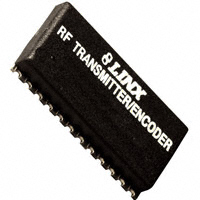
1.220"
0.630"
RF TRANSMITTER/ENCODER TXE-418-KH2
LOT 10000
0.180"
Figure 1: Package Dimensions
FEATURES
Low cost On-board encoder 8 parallel binary inputs 310 addresses for security and uniqueness No external RF components required Ultra-low power consumption Compact SMD package Stable SAW-based architecture Adjustable output power Transmit enable line No production tuning
APPLICATIONS INCLUDE
Remote Control / Command Keyless Entry Garage / Gate Openers Lighting Control Call Systems Home / Industrial Automation Fire / Security Alarms Remote Status Monitoring Wire Elimination
ORDERING INFORMATION
PART # DESCRIPTION TXE-315-KH2 Transmitter 315MHz TXE-418-KH2 Transmitter 418MHz TXE-433-KH2 Transmitter 433MHz RXD-315-KH2 Receiver 315MHz RXD-418-KH2 Receiver 418MHz RXD-433-KH2 Receiver 433MHz EVAL-***-KH2 Basic Evaluation Kit *** = 315, 418 (Standard), 433.92MHz. Transmitters are supplied in tubes of 20 pcs.
Revised 1/28/08
�ELECTRICAL SPECIFICATIONS
Parameter POWER SUPPLY Operating Voltage Supply Current Power-Down Current TRANSMITTER SECTION Transmit Frequency Range: TXE-315-KH2 TXE-418-KH2 TXE-433-KH2 Center Frequency Accuracy Output Power Harmonic Emissions: TXE-315-KH2 TXE-418-KH2 TXE-433-KH2 ANTENNA PORT RF Output Impedance ENCODER SECTION Data Length Average Data Duty Cycle Encoder Oscillator Data Input: Logic Low Logic High Input Sink Current ENVIRONMENTAL Operating Temperature Range – -30 – +70 – – – FENC – – – – 0.0 VCC x 0.8 0.6 26 bits 3x 50% 70 – – 1.0 – – – 0.2 x VCC VCC 1.2 – – kHz VDC VDC mA – 4 4 4 4 4 4 ROUT – 50 – Ω 4 – PO PH -40 -40 -45 – – – – – – dBc dBc dBc – – – FC – – – -75 -4 315 418 433.92 – +2 – – – +75 +4 MHz MHz MHz kHz dBm – – – – 2,3 VCC ICC IPDN 2.7 – – – 1.5 1.0 5.2 – – VDC mA µA – 1,4 – Designation Min. Typical Max. Units Notes
ABSOLUTE MAXIMUM RATINGS
Supply Voltage VCC Any Input or Output Pin Operating Temperature Storage Temperature Soldering Temperature -0.3 -0.3 -30 -45 +225°C to +6.0 to VCC to +70 to +85 for 10 seconds VDC VDC °C °C
*NOTE* Exceeding any of the limits of this section may lead to permanent damage to the device. Furthermore, extended operation at these maximum ratings may reduce the life of this device.
PERFORMANCE DATA
These performance parameters are based on module operation at 25°C from a 3.0VDC supply unless otherwise noted. Figure 2 illustrates the connections necessary for testing and operation. It is recommended all ground pins be connected to the ground plane.
VCC 1 2 3VDC 3 4 5 6 7 8 9 10 11 12 24 23 22 21 20 19 18 17 16 15 14 13 LADJ/GND ANT D0 GND D1 A9 GND A8 VCC A7 TE A6 D2 A5 D3 A4 D4 A3 D5 A2 D6 A1 D7 A0
Figure 2: Test / Basic Application Circuit
TYPICAL PERFORMANCE GRAPHS
12 11 10 9 8 7 6 5 4 3 2 1 0 2.5
+8 +7 +6 +5 +4 +3 +2 +1 0 -1 -2 -3 -4 -5 -6 -7
°C
Table 1: KH2 Series Transmitter Electrical Specifications
With LADJ tied to ground
Notes
1. 2. 3. 4. Current draw with 50% mark / space ratio. Into a 50Ω load. With 430Ω resistor on LADJ. Characterized, but not tested.
Output Power Into 50 ohms (dBm)
With LADJ tied to ground
Supply Current (mA)
With 430Ω resistor on LADJ
With 430Ω resistor on LADJ 4.0 4.5 3.0 3.5 Supply Voltage (V) 5.0
2.5
4.0 4.5 3.0 3.5 Supply Voltage (V)
5.0
Figure 3: Supply Current vs. Supply Voltage
+8 +7
Figure 4: Output Power vs. Supply Voltage
*CAUTION*
This product incorporates numerous static-sensitive components. Always wear an ESD wrist strap and observe proper ESD handling procedures when working with this device. Failure to observe this precaution may result in module damage or failure.
Output Power (dBm)
+6 +5 +4 +3 +2 +1 0 -1 -2 -3 -4
5V 3V
51 100 150 200 240 300 360 430 510 560 620 680 750 820 910 1.1K
LADJ Pin Resistor Value (Ω)
Figure 5: Output Power vs. LADJ Resistor
Page 2 Page 3
�PIN ASSIGNMENTS
1 2 3 4 5 6 7 8 9 10 11 12 LADJ/GND ANT D0 GND D1 A9 GND A8 VCC A7 TE A6 D2 A5 D3 A4 A3 D4 A2 D5 D6 A1 D7 A0 24 23 22 21 20 19 18 17 16 15 14 13
MODULE DESCRIPTION
The KH2 Series transmitter / encoder module combines a high-performance Surface Acoustic Wave (SAW) based transmitter with an on-board encoder. When combined with a Linx KH2 Series receiver / decoder, a highly reliable RF link capable of transferring control or command data over line-of-sight distances of up to 3,000 feet is formed. The module accepts up to 8 parallel inputs, such as switches or contact closures, and provides ten tri-state address lines for security and creation of 59,049 (310) unique transmitter / receiver relationships. The KH’s compact surface-mount package integrates easily into existing designs and is friendly to hand production or automated assembly.
Address Inputs A0-A9 50Ω RF OUT (ANT) Keyed Output Buffer SAW Oscillator TX Enable Divider Sync Counter OSC GATE Parallel Inputs D0-D7
Figure 6: KH2 Series Transmitter Pinout (Top View)
PIN DESCRIPTIONS Pin #
1
TRI-Detect
Name
Description
Output Isolation & Filter
RF Amplifier
Level Adjust. This line can be used to adjust the output power level of the transmitter. Connecting to GND will give GND / LADJ the highest output, while placing a resistor to GND will lower the output level. Data Input Lines. When TE goes high, the module will encode the state of these lines for transmission. Upon receipt of a valid transmission, the receiver / decoder will replicate these lines on its output lines. Analog Ground Supply Voltage Transmit Enable Line. When this line goes high, the module will encode the states of the address and data lines into a packet and transmit the packet three times. Address Lines. The state of these lines must match the state of the receiver’s address lines in order for a transmission to be accepted. Analog Ground 50-ohm RF Output
RF STAGE
THEORY OF OPERATION
ENCODER STAGE
Figure 7: KH2 Series Transmitter Block Diagram
2, 3, 7-12 4 5
D0 - D1
GND VCC
The KH2 Series transmitter operation is straightforward. When the Transmit Enable (TE) line is taken high, the on-board encoder IC is activated. The encoder detects the logic states of the data and address lines. These states are formatted into a 3-word transmission, which continues until the TE line is taken low. The encoder creates a serial data packet that is used to modulate the transmitter. The transmitter section is based on a simple, but highly-optimized, architecture that achieves a high fundamental output power with low harmonic content. This ensures that most approval standards can be met without external filter components. The KH2 Series transmitter is exceptionally stable over variations in time, temperature, and physical shock as a result of the precision SAW device that is incorporated as the frequency reference. The transmitted signal may be received by a Linx KH2 Series receiver / decoder module or a Linx LR Series receiver combined with the appropriate decoder IC. Once data is received, it is decoded using a decoder IC or custom microcontroller. The transmitted address bits are checked against the address settings of the receiving device. If a match is confirmed, the decoder’s outputs are set to replicate the transmitter’s inputs.
6
TE
13-22
A0-A9
23 24
GND ANT
Page 4
Page 5
�ENCODER OPERATION
The KH2 Series transmitter internally utilizes the HT640 encoder from Holtek. The encoder begins a three-word transmission cycle when the Transmission Enable line (TE) is pulled high. This cycle will repeat itself for as long as the TE line is held high. Once TE falls low, the encoder output completes its final cycle and then stops as shown in the Encoder / Decoder Timing diagram. When a transmission enable signal is applied, the encoder scans and transmits the status of the 10 bits of the address code and the 8 bits of the data serially in the order A0 to A9, D0 to D7.
Power On
POWER SUPPLY REQUIREMENTS
The module does not have an internal voltage regulator; therefore it requires a clean, well-regulated power source. While it is preferable to power the unit from a battery, it can also be operated from a power supply as long as noise is less than 20mV. Power supply noise can affect the transmitter modulation; therefore, providing a clean power supply for the module should be a high priority during design.
Vcc TO MODULE 10Ω Vcc IN
+
Standby Mode
10μF
No
Transmission Enabled? Yes 3 Data Words Transmitted
A 10Ω resistor in series with the supply followed by a Figure 10: Supply Filter 10µF tantalum capacitor from VCC to ground will help in cases where the quality of supply power is poor. These values may need to be adjusted depending on the noise present on the supply line.
DATA INPUTS
Transmission Still Enabled?
The status of each address / data pin can be individually preset to logic high, low, or floating. The floating state on the data input is interpreted as logic low by the decoders 3 Data Words Transmitted since the decoder output only has two Continuously states. The address pins are usually set to transmit particular security codes by DIP switches or PCB wiring, while the data is Figure 8: Encoder Flowchart selected using push buttons or electronic switches. The floating state allows the KH2 transmitter to be used without pullup or pull-down resistors on the data and address input lines.
Encoder Transmit Enable Encoder Data Out
3 Words 2 Words Check Check
When the Transmit Enable (TE) line goes high, the states of the eight data input lines are recorded and encoded for transmission. The data lines are tri-state, which means that they can be high, low, or floating, though the decoder will interpret the floating state as a low. This feature means that the data lines do not require pull-up or pull-down resistors. The states of the data lines can be set by switches, jumpers, microcontrollers, or hardwired on the PCB. The encoder will send the states of the address and data lines three times. If the TE line is still high, it will begin the cycle again. This means that the states of the data lines are refreshed with each cycle, so the data lines can be changed without having to pull TE low. There can be up to a 150mS lag in response as the transmitter finishes one cycle then refreshes and starts over.
ENABLING TRANSMISSION
< 1 Word
Transmitted Continuously 14 2 Clocks
3 Words 2 14 Clocks
Decoder VT Decoder Data Out
The module’s Transmit Enable (TE) line controls transmission status. When taken high, the module initiates transmission, which continues until the line is pulled low or power to the module is removed. In some cases this line will be wired permanently to VCC and transmission controlled by switching VCC to the module. This is particularly useful in applications where the module powers up and sends a transmission only when a button is pressed on the remote.
USING LADJ
1/2 Clock Time 1/2 Clock Time
Figure 9: Encoder / Decoder Timing Diagram
SETTING THE TRANSMITTER ADDRESS
The module provides ten tri-state address lines. This allows for the formation of up to 59,049 (310) unique transmitter-receiver relationships. Tri-state means that the address lines have three distinct states: high, low, or floating. These pins may be hardwired or configured via a microprocessor, DIP switch, or jumpers. The receiver’s address line states must match the transmitter’s exactly for a transmission to be recognized. If the transmitted address does not match the receiver’s local address, then the receiver will take no action.
Page 6
The LADJ line allows the transmitter’s output power to be easily adjusted for range control, lower power consumption, or to meet legal requirements. This is done by placing a resistor between GND and LADJ. When LADJ is connected directly to GND, the output power will be at its maximum. Placing a resistor will lower the output power by up to 7dB, as shown on Page 3 of this data guide. This is very useful during FCC testing to compensate for antenna gain or other product-specific issues that may cause the output power to exceed legal limits. A variable resistor can be used so that the test lab can precicely adjust the output power to the maximun level allowed by law. The resistor’s value can be noted and a fixed resistor substituted for final testing. Even in designs where attenuation is not anticipated, it is a good idea to place a resistor pad connected to LADJ and GND so that it can be used if needed.
Page 7
�PROTOCOL GUIDELINES
While many RF solutions impose data formatting and balancing requirements, Linx RF modules do not encode or packetize the signal content in any manner. The received signal will be affected by such factors as noise, edge jitter, and interference, but it is not purposefully manipulated or altered by the modules. This gives the designer tremendous flexibility for protocol design and interface. Despite this transparency and ease of use, it must be recognized that there are distinct differences between a wired and a wireless environment. Issues such as interference and contention must be understood and allowed for in the design process. To learn more about protocol considerations, we suggest you read Linx Application Note AN-00160. Errors from interference or changing signal conditions can cause corruption of the data packet, so it is generally wise to structure the data being sent into small packets. This allows errors to be managed without affecting large amounts of data. A simple checksum or CRC could be used for basic error detection. Once an error is detected, the protocol designer may wish to simply discard the corrupt data or implement a more sophisticated scheme to correct it.
TYPICAL APPLICATIONS
Below is an example of a basic remote control transmitter utilizing the KH2 Series transmitter. When a key is pressed on the transmitter, a corresponding line on the receiver goes high. A schematic for the receiver / decoder circuit may be found in the KH2 Series Receiver Data Guide. These circuits are implemented in the KH2 Series Basic Evaluation kit. They can be easily modified for custom applications and clearly demonstrate the ease of using the KH2 Series modules for remote control applications.
VCC
VCC
SW0
R1 1 2 3 GND/LADJ D0 D1 GND VCC TE D2 D3 D4 D5 D6 D7 TXE-xxx-KH2 ANT GND A9 A8 A7 A6 A5 A4 A3 A2 A1 A0 24 23 22 21 20 19 18 17 SW-DIP-10 16 15 14 13 GND GND 1 2 3 4 5 6 7 8 9 10 20 19 18 17 16 15 14 13 12 11
SW-SPDT
GND
0 OHM
VCC
SW1
VCC GND
4 5 6 7 8 9 10 11 12
SW-SPDT
INTERFERENCE CONSIDERATIONS
The RF spectrum is crowded and the potential for conflict with other unwanted sources of RF is very real. While all RF products are at risk from interference, its effects can be minimized by better understanding its characteristics. Interference may come from internal or external sources. The first step is to eliminate interference from noise sources on the board. This means paying careful attention to layout, grounding, filtering, and bypassing in order to eliminate all radiated and conducted interference paths. For many products, this is straightforward; however, products containing components such as switching power supplies, motors, crystals, and other potential sources of noise must be approached with care. Comparing your own design with a Linx evaluation board can help to determine if and at what level design-specific interference is present. External interference can manifest itself in a variety of ways. Low-level interference will produce noise and hashing on the output and reduce the link’s overall range. High-level interference is caused by nearby products sharing the same frequency or from near-band high-power devices. It can even come from your own products if more than one transmitter is active in the same area. It is important to remember that only one transmitter at a time can occupy a frequency, regardless of the coding of the transmitted signal. This type of interference is less common than those mentioned previously, but in severe cases it can prevent all useful function of the affected device. Although technically it is not interference, multipath is also a factor to be understood. Multipath is a term used to refer to the signal cancellation effects that occur when RF waves arrive at the receiver in different phase relationships. This effect is a particularly significant factor in interior environments where objects provide many different signal reflection paths. Multipath cancellation results in lowered signal levels at the receiver and, thus, shorter useful distances for the link.
Page 8
R2 100K
VCC
VCC + C1 10uF
CR2032 3V LITHIUM
GND
GND
GND
Figure 11: Basic Remote Control Transmitter
The ten-position DIP switch is used to set the address to either ground or floating. Since the floating state is a valid state, no pull-up resistors are needed. The data lines are pulled high by momentary pushbuttons. Since the floating state is interpreted as a low by the decoder, no pull-down resistors are needed. Diodes are used to pull the TE line high when any data line goes high, while isolating the data lines from each other. This will make the transmitter send data when any button is pressed without affecting any of the other data lines. The KH2 Series transmitter / encoder module is also suitable for use with the Linx OEM function receivers. These receivers are FCC certified, making product introduction extremely quick. Information on these products can be found on the Linx website at www.linxtechnologies.com.
Page 9
�BOARD LAYOUT GUIDELINES
If you are at all familiar with RF devices, you may be concerned about specialized board layout requirements. Fortunately, because of the care taken by Linx in designing the modules, integrating them is very straightforward. Despite this ease of application, it is still necessary to maintain respect for the RF stage and exercise appropriate care in layout and application in order to maximize performance and ensure reliable operation. The antenna can also be influenced by layout choices. Please review this data guide in its entirety prior to beginning your design. By adhering to good layout principles and observing some basic design rules, you will be on the path to RF success. The adjacent figure shows the suggested PCB footprint for the module. The actual pad dimensions are shown in the Pad Layout section of this manual. A ground plane (as large as possible) should be placed on a lower layer of your PC board opposite the module. This ground plane can also be critical to the performance of your antenna, which will be discussed later. There should not be any ground or traces under the module on the same layer as the module, just bare PCB.
GROUND PLANE ON LOWER LAYER
MICROSTRIP DETAILS
A transmission line is a medium whereby RF energy is transferred from one place to another with minimal loss. This is a critical factor, especially in highfrequency products like Linx RF modules, because the trace leading to the module’s antenna can effectively contribute to the length of the antenna, changing its resonant bandwidth. In order to minimize loss and detuning, some form of transmission line between the antenna and the module should be used, unless the antenna can be placed very close ( the overall length of the 1/4-wave PLANE VIRTUAL λ/4 radiating element. This is often not practical due to DIPOLE size and configuration constraints. In these instances, a designer must make the best use of the Figure 20: Dipole Antenna area available to create as much ground plane as possible in proximity to the base of the antenna. In cases where the antenna is remotely located or the antenna is not in close proximity to a circuit board, ground plane, or grounded metal case, a metal plate may be used to maximize the antenna’s performance.
E
λ/4
I
λ/4
ANTENNA SHARING
In cases where a transmitter and receiver VDD module are combined to form a transceiver, Transmitter 0.1μF it is often advantageous to share a single Module 0.1μF Antenna antenna. To accomplish this, an antenna 0.1μF GND switch must be used to provide isolation 0.1μF between the modules so that the full GND Receiver Module transmitter output power is not put on the 0.1μF sensitive front end of the receiver. There Select are a wide variety of antenna switches that Figure 18: Typical Antenna Switch are cost-effective and easy to use. Among the most popular are switches from Macom and NEC. Look for an antenna switch that has high isolation and low loss at the desired frequency of operation. Generally, the Tx or Rx status of a switch will be controlled by a product’s microprocessor, but the user may also make the selection manually. In some cases, where the characteristics of the Tx and Rx antennas need to be different or antenna switch losses are unacceptable, it may be more appropriate to utilize two discrete antennas.
Page 14
5. Remove the antenna as far as possible from potential interference sources. Any frequency of sufficient amplitude to enter the receiver’s front end will reduce system range and can even prevent reception entirely. Switching power supplies, oscillators, or even relays can also be significant sources of potential interference. The single best weapon against such problems is attention to placement and layout. Filter the module’s power supply with a high-frequency bypass capacitor. Place adequate ground plane under potential sources of noise to shunt noise to ground and prevent it from coupling to the RF stage. Shield noisy board areas whenever practical. 6. In some applications, it is advantageous to place the module and antenna away from the main equipment. This can avoid interference problems and allows the antenna to be oriented for optimum performance. Always use 50Ω coax, like RG-174, for the remote feed.
CASE GROUND PLANE (MAY BE NEEDED)
NUT
Figure 21: Remote Ground Plane
Page 15
�COMMON ANTENNA STYLES
There are literally hundreds of antenna styles and variations that can be employed with Linx RF modules. Following is a brief discussion of the styles most commonly utilized. Additional antenna information can be found in Linx Application Notes AN-00100, AN-00140, and AN-00500. Linx antennas and connectors offer outstanding performance at a low price.
ONLINE RESOURCES
®
Whip Style
A whip-style antenna provides outstanding overall performance and stability. A low-cost whip is can be easily fabricated from a wire or rod, but most designers opt for the consistent performance and cosmetic appeal of a professionally-made model. To meet this need, Linx offers a wide variety of straight and reduced-height whip-style antennas in permanent and connectorized mounting styles. The wavelength of the operational frequency determines an antenna’s overall length. Since a full wavelength is often quite long, a partial 1/2- or 1/4-wave antenna is normally employed. Its size and natural radiation resistance make it well matched to Linx modules. The proper length for a straight 1/4-wave can be easily determined using the adjacent formula. It is also possible to reduce the overall height of the antenna by using a helical winding. This reduces the antenna’s bandwidth, but is a great way to minimize the antenna’s physical size for compact applications. This also means that the physical appearance is not always an indicator of the antenna’s frequency. Linx offers a wide variety of specialized antenna styles. Many of these styles utilize helical elements to reduce the overall antenna size while maintaining reasonable performance. A helical antenna’s bandwidth is often quite narrow and the antenna can detune in proximity to other objects, so care must be exercised in layout and placement.
www.linxtechnologies.com
• • • • •
Latest News Data Guides Application Notes Knowledgebase Software Updates
L=
234
F MHz
Where: L = length in feet of quarter-wave length F = operating frequency in megahertz
If you have questions regarding any Linx product and have Internet access, make www.linxtechnologies.com your first stop. Our website is organized in an intuitive format to immediately give you the answers you need. Day or night, the Linx website gives you instant access to the latest information regarding the products and services of Linx. It’s all here: manual and software updates, application notes, a comprehensive knowledgebase, FCC information, and much more. Be sure to visit often!
Specialty Styles
www.antennafactor.com The Antenna Factor division of Linx offers a diverse array of antenna styles, many of which are optimized for use with our RF modules. From innovative embeddable antennas to low-cost whips, domes to Yagis, and even GPS, Antenna Factor likely has an antenna for you, or can design one to meet your requirements.
Loop Style
A loop- or trace-style antenna is normally printed directly on a product’s PCB. This makes it the most cost-effective of antenna styles. The element can be made self-resonant or externally resonated with discrete components, but its actual layout is usually product specific. Despite the cost advantages, loop-style antennas are generally inefficient and useful only for short-range applications. They are also very sensitive to changes in layout and PCB dielectric, which can cause consistency issues during production. In addition, printed styles are difficult to engineer, requiring the use of expensive equipment, including a network analyzer. An improperly designed loop will have a high SWR at the desired frequency, which can cause instability in the RF stage. Linx offers low-cost planar and chip antennas that mount directly to a product’s PCB. These tiny antennas do not require testing and provide excellent performance in light of their small size. They offer a preferable alternative to the often-problematic “printed” antenna.
www.connectorcity.com Through its Connector City division, Linx offers a wide selection of high-quality RF connectors, including FCCcompliant types such as RP-SMAs that are an ideal match for our modules and antennas. Connector City focuses on high-volume OEM requirements, which allows standard and custom RF connectors to be offered at a remarkably low cost.
Page 17
Page 16
�LEGAL CONSIDERATIONS
NOTE: Linx RF modules are designed as component devices that require external components to function. The modules are intended to allow for full Part 15 compliance; however, they are not approved by the FCC or any other agency worldwide. The purchaser understands that approvals may be required prior to the sale or operation of the device, and agrees to utilize the component in keeping with all laws governing its use in the country of operation.
When working with RF, a clear distinction must be made between what is technically possible and what is legally acceptable in the country where operation is intended. Many manufacturers have avoided incorporating RF into their products as a result of uncertainty and even fear of the approval and certification process. Here at Linx, our desire is not only to expedite the design process, but also to assist you in achieving a clear idea of what is involved in obtaining the necessary approvals to legally market your completed product. In the United States, the approval process is actually quite straightforward. The regulations governing RF devices and the enforcement of them are the responsibility of the Federal Communications Commission (FCC). The regulations are contained in Title 47 of the Code of Federal Regulations (CFR). Title 47 is made up of numerous volumes; however, all regulations applicable to this module are contained in Volume 0-19. It is strongly recommended that a copy be obtained from the Government Printing Office in Washington or from your local government bookstore. Excerpts of applicable sections are included with Linx evaluation kits or may be obtained from the Linx Technologies website, www.linxtechnologies.com. In brief, these rules require that any device that intentionally radiates RF energy be approved, that is, tested for compliance and issued a unique identification number. This is a relatively painless process. Linx offers full EMC precompliance testing in our HP / Emco-equipped test center. Final compliance testing is then performed by one of the many independent testing laboratories across the country. Many labs can also provide other certifications that the product may require at the same time, such as UL, CLASS A / B, etc. Once your completed product has passed, you will be issued an ID number that is to be clearly placed on each product manufactured. Questions regarding interpretations of the Part 2 and Part 15 rules or measurement procedures used to test intentional radiators, such as Linx RF modules, for compliance with the technical standards of Part 15, should be addressed to: Federal Communications Commission Equipment Authorization Division Customer Service Branch, MS 1300F2 7435 Oakland Mills Road Columbia, MD 21046 Phone: (301) 725-1585 Fax: (301) 344-2050 E-Mail: labinfo@fcc.gov International approvals are slightly more complex, although Linx modules are designed to allow all international standards to be met. If you are considering the export of your product abroad, you should contact Linx Technologies to determine the specific suitability of the module to your application. All Linx modules are designed with the approval process in mind and thus much of the frustration that is typically experienced with a discrete design is eliminated. Approval is still dependent on many factors, such as the choice of antennas, correct use of the frequency selected, and physical packaging. While some extra cost and design effort are required to address these issues, the additional usefulness and profitability added to a product by RF makes the effort more than worthwhile.
Page 18
ACHIEVING A SUCCESSFUL RF IMPLEMENTATION
Adding an RF stage brings an exciting new dimension to any product. It also means that additional effort and commitment will be needed to bring the product successfully to market. By utilizing premade RF modules, such as the LR Series, the design and approval process is greatly simplified. It is still important, however, to have an objective view of the steps necessary to ensure a successful RF integration. Since the capabilities of each customer vary widely, it is difficult to recommend one particular design path, but most projects follow steps similar to those shown at the right.
DECIDE TO UTILIZE RF
RESEARCH RF OPTIONS ORDER EVALUATION KIT(S)
TEST MODULE(S) WITH BASIC HOOKUP CHOOSE LINX MODULE INTERFACE TO CHOSEN CIRCUIT AND DEBUG CONSULT LINX REGARDING ANTENNA OPTIONS AND DESIGN LAY OUT BOARD
In reviewing this sample design path, you may SEND PRODUCTION-READY PROTOTYPE TO LINX FOR EMC PRESCREENING notice that Linx offers a variety of services (such as antenna design and FCC prequalification) that are OPTIMIZE USING RF SUMMARY GENERATED BY LINX unusual for a high-volume component manufacturer. SEND TO PART 15 These services, along with an exceptional level of TEST FACILITY technical support, are offered because we recognize RECEIVE FCC ID # that RF is a complex science requiring the highest caliber of products and support. “Wireless Made COMMENCE SELLING PRODUCT Simple” is more than just a motto, it’s our Typical Steps For commitment. By choosing Linx as your RF partner Implementing RF and taking advantage of the resources we offer, you will not only survive implementing RF, you may even find the process enjoyable.
HELPFUL APPLICATION NOTES FROM LINX
It is not the intention of this manual to address in depth many of the issues that should be considered to ensure that the modules function correctly and deliver the maximum possible performance. As you proceed with your design, you may wish to obtain one or more of the following application notes, which address in depth key areas of RF design and application of Linx products. These applications notes are available online at www.linxtechnologies.com or by contacting the Linx literature department.
NOTE
AN-00100 AN-00125 AN-00130 AN-00140 AN-00150 AN-00160 AN-00300 AN-00500
APPLICATION NOTE TITLE
RF 101: Information for the RF Challenged Considerations For Operation Within The 260-470MHz Band Modulation Techniques For Low-Cost RF Data Links The FCC Road: Part 15 From Concept To Approval Use and Design of T-Attenuation Pads Considerations For Sending Data Over a Wireless Link Addressing Linx OEM Products Antennas: Design, Application, Performance
Page 19
�WIRELESS MADE SIMPLE ®
U.S. CORPORATE HEADQUARTERS
LINX TECHNOLOGIES, INC.
159 ORT LANE MERLIN, OR 97532
PHONE: (541) 471-6256 FAX: (541) 471-6251
www.linxtechnologies.com
Disclaimer
Linx Technologies is continually striving to improve the quality and function of its products. For this reason, we reserve the right to make changes to our products without notice. The information contained in this Overview Guide is believed to be accurate as of the time of publication. Specifications are based on representative lot samples. Values may vary from lot-to-lot and are not guaranteed. "Typical" parameters can and do vary over lots and application. Linx Technologies makes no guarantee, warranty, or representation regarding the suitability of any product for use in any specific application. It is the customer's responsibility to verify the suitability of the part for the intended application. NO LINX PRODUCT IS INTENDED FOR USE IN ANY APPLICATION WHERE THE SAFETY OF LIFE OR PROPERTY IS AT RISK. Linx Technologies DISCLAIMS ALL WARRANTIES OF MERCHANTABILITY AND FITNESS FOR A PARTICULAR PURPOSE. IN NO EVENT SHALL LINX TECHNOLOGIES BE LIABLE FOR ANY OF CUSTOMER'S INCIDENTAL OR CONSEQUENTIAL DAMAGES ARISING IN ANY WAY FROM ANY DEFECTIVE OR NON-CONFORMING PRODUCTS OR FOR ANY OTHER BREACH OF CONTRACT BY LINX TECHNOLOGIES. The limitations on Linx Technologies' liability are applicable to any and all claims or theories of recovery asserted by Customer, including, without limitation, breach of contract, breach of warranty, strict liability, or negligence. Customer assumes all liability (including, without limitation, liability for injury to person or property, economic loss, or business interruption) for all claims, including claims from third parties, arising from the use of the Products. The Customer will indemnify, defend, protect, and hold harmless Linx Technologies and its officers, employees, subsidiaries, affiliates, distributors, and representatives from and against all claims, damages, actions, suits, proceedings, demands, assessments, adjustments, costs, and expenses incurred by Linx Technologies as a result of or arising from any Products sold by Linx Technologies to Customer. Under no conditions will Linx Technologies be responsible for losses arising from the use or failure of the device in any application, other than the repair, replacement, or refund limited to the original product purchase price. Devices described in this publication may contain proprietary, patented, or copyrighted techniques, components, or materials. Under no circumstances shall any user be conveyed any license or right to the use or ownership of such items.
© 2008 by Linx Technologies, Inc. The stylized Linx logo, Linx, “Wireless Made Simple”, CipherLinx, and the stylized CL logo are the trademarks of Linx Technologies, Inc. Printed in U.S.A.
�