HIGH-PERFORMANCE
RF MODULE
TXM-900-HP3-xxx
WIRELESS MADE SIMPLE ®
HP3 SERIES TRANSMITTER MODULE DATA GUIDE
DESCRIPTION
The HP3 RF transmitter module is the third generation of the popular HP Series. Like its 0.680" predecessors, the HP3 is designed for the costeffective, high-performance wireless transfer of analog or digital information in the popular 9020.178" 928MHz band. HP3 Series parts feature eight SIP Style parallel selectable channels, and some versions 1.260" also add direct serial selection of 100 channels. To ensure reliable performance, the transmitter 0.628" employs FM / FSK modulation and a microprocessor controlled synthesized architecture. 0.150" Both SMD and pinned packages are available. SMD Style When paired with an HP3 receiver, a reliable Figure 1: Package Dimensions link is created for the transfer of analog and digital information up to 1,000 feet. As with all Linx modules, the HP3 requires no tuning or additional RF components (except an antenna), making integration straightforward, even for engineers without prior RF experience.
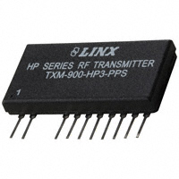
HP SERIES RF TRANSMITTER TXM-900-HP3-SP* LOT 10000 Pin Spacing: 0.1" HP SERIES RF TRANSMITTER TXM-900-HP3-SP* LOT 10000
1.290"
FEATURES
APPLICATIONS INCLUDE
8 parallel, 100 serial (PS Versions) userWireless Networks / Data Transfer selectable channels Wireless Analog / Audio FM / FSK modulation for outstanding Home / Industrial Automation performance and noise immunity Remote Access / Control Precision frequency synthesized Remote Monitoring / Telemetry architecture Long-Range RFID Transparent analog / digital interface MIDI Links Wide-range analog capability including audio (50Hz to 28kHz) Voice / Music / Intercom Links Wide temperature range (-30°C to +85°C) ORDERING INFORMATION No external RF PART # DESCRIPTION components required HP3 Transmitter (SIP 8 CH only) Compatible with previous TXM-900-HP3-PPO HP Series modules TXM-900-HP3-PPS HP3 Transmitter (SIP 8p / 100s CH) Power-down and CTS TXM-900-HP3-SPO HP3 Transmitter (SMD 8 CH only) functions TXM-900-HP3-SPS HP3 Transmitter (SMD 8p / 100s CH) Wide supply range MDEV-900-HP3-PPS-USB HP3 Development Kit (SIP Pkg.) (2.8 to 13.0VDC) MDEV-900-HP3-PPS-RS232 HP3 Development Kit (SIP Pkg.) High data rate MDEV-900-HP3-SPS-USB HP3 Development Kit (SMD Pkg.) (up to 56kbps) MDEV-900-HP3-SPS-RS232 HP3 Development Kit (SMD Pkg.) Pinned and SMD packages Transmitters are supplied in tubes of 15 pcs. No production tuning
Revised 1/28/08
�ELECTRICAL SPECIFICATIONS
Parameter POWER SUPPLY Operating Voltage Supply Current Power-Down Current TRANSMIT SECTION Transmit Frequency Range Center Frequency Accuracy Available Channels Channel Spacing Occupied Bandwidth Output Power Spurious Emissions Harmonic Emissions Data Rate Analog / Audio Bandwidth Data Input: Logic Low Logic High Data Input Impedance Frequency Deviation @ 3VDC Frequency Deviation @ 5VDC ANTENNA PORT RF Output Impedance TIMING Transmitter Turn-On Time Channel Change Time ENVIRONMENTAL Operating Temperature Range – -30 – +85 – – – – 7.0 1.0 10.0 1.5 mSec mSec – – ROUT – 50 – Ω – – – – – – 0.0 2.8 – 60 90 – – 200 70 115 0.5 5.2 – 110 140 VDC VDC kΩ kHz kHz – – – 8 8 FC – – – – PO – PH – – 902.62 -50 8 (Par.) – – -3 – – 100 50 – – – 250 115 0 -45 -60 – – 927.62 +50 100 (Ser.) – 140 +3 – -47 56,000 28,000 MHz kHz – kHz kHz dBm dBm dBm bps Hz 3 – 4 – – 5 6 6 7 7 VCC ICC IPDN 2.8 – – 3.0 14.0 – 13.0 17.0 15.0 VDC mA µA – 1 2 Designation Min. Typical Max. Units Notes
ABSOLUTE MAXIMUM RATINGS
Supply Voltage VCC Any Input or Output Pin Operating Temperature Storage Temperature Soldering Temperature -0.3 -0.3 -30 -45 +260°C to +18.0 to VCC to +85 to +85 for 10 seconds VDC VDC °C °C
*NOTE* Exceeding any of the limits of this section may lead to permanent damage to the device. Furthermore, extended operation at these maximum ratings may reduce the life of this device.
PERFORMANCE DATA
These performance parameters are based on module operation at 25°C from a 5.0VDC supply unless otherwise noted. Figure 2 illustrates the connections necessary for testing and operation. It is recommended all ground pins be connected to the ground plane. The pins marked NC have no electrical connection.
GND ANT GND NC CS0 CS1 / SS CLOCK CS2 / SS D CTS PDN VCC MODE DATA NC NC NC NC GND NC NC NC NC NC NC GND
PC PC PC 5VDC
PC
Figure 2: Test / Basic Application Circuit
TYPICAL PERFORMANCE GRAPHS
VCC / PDN
VCC / PDN
°C
–
Table 1: HP3 Series Transmitter Specifications
Notes
1. 2. 3. 4. 5. 6. 7. Over the entire operating voltage range. With the PDN pin low. Serial Mode. 100 serial channels on the PS versions only. Does not change over the 3-13VDC supply. Into 50 ohms. The receiver will not reliably hold a DC level. See the HP3 Series Receiver Module Data Guide for the minimum transition rate. 8. The voltage specified is the modulation pin voltage.
1
1
RX DATA
CTS
2 CH1 1.00V CH2 2.00V 2.5mS Delta 7.200mS
2 CH1 1.00V CH2 2.00V 2.5mS Delta 7.200mS
Figure 3: Power-Up to CTS
Figure 4: TX Powerup to Valid RX Data
IN
IN
*CAUTION*
This product incorporates numerous static-sensitive components. Always wear an ESD wrist strap and observe proper ESD handling procedures when working with this device. Failure to observe this precaution may result in module damage or failure.
OUT
OUT
CH1 2.00V
CH2 500mV
250μS
CH1 2.00V
CH2 500mV
250μS
Figure 5: Sine Wave Modulation Linearity
Page 2
Figure 6: Square Wave Modulation Linearity
Page 3
�PIN ASSIGNMENTS
Pinned Transmitter
3 CS0 4 CS1 / SS CLOCK 5 CS 2 / SS DATA 6 CTS
PIN DESCRIPTIONS
Surface-Mount Transmitter
1 2 3 4 5 6 7 8 9 10 11 12 GND ANT GND NC CS0 CS1 / SS CLOCK CS2 / SS DATA CTS PDN VCC MODE DATA NC NC NC NC GND NC NC NC NC NC NC GND 24 23 22 21 20 19 18 17 16 15 14 13
Pin # SMD Pinned 1, 3 13, 20 1
Name GND
Equivalent Circuit
Description Analog Ground
9 MODE 10 DATA
1 GND 2 ANT
7 PDN 8 VCC
2
2
ANT
RF Out
50Ω 50-ohm RF Output
5
3
CS0 CS0
25k
Channel Select 0
µ Channel Select 1 / Serial Select Clock Channel Select 2 / Serial Select Data
Figure 7: HP3 Series Receiver Pinout
Pin #
SMD SIP 1 2 3 4 5 6 3 4 1 2
6
4
CS1 / SS CLOCK
25k
Name
GND ANT GND NC CS0 CS1 / SS CLOCK CS2 / SS DATA CTS
Description
Analog Ground 50-ohm RF Output Analog Ground (SMD only) No Electrical Connection. Soldered for physical support only. Channel Select 0 Channel Select 1 / Serial Select Clock. Channel Select 1 when in parallel channel selection mode, clock input for serial channel selection mode. Channel Select 2 / Serial Select Data. Channel Select 2 when in parallel channel selection mode, data input for serial channel selection mode. Clear-To-Send. This line will go high when the transmitter is ready to accept data. Power Down. Pulling this line low will place the receiver into a low-current state. The module will not be able to receive a signal in this state. Supply Voltage Mode Select. GND for parallel channel selection, VCC for serial channel selection Digital / Analog Data Input. This line will output the demodulated digital data. Analog Ground (SMD only) No Electrical Connection. Soldered for physical support only. (SMD only)
8 6 CTS 7 5 CS2 / SS DATA
CS1
µ
25k
CS2
µ
CTS Out
Clear-to-Send Output
VCC 430k 9 7 PDN PDN Power Down (Active Low)
7
5
8
6
10
8
VCC
Voltage Input 2.8-13V
9 10 11 12 13, 20 14-19, 21-24
Page 4
7 8 9 10
PDN VCC MODE DATA GND NC
11
9
MODE MODE
160k
25k
Mode Select
µ
100k
12
10
DATA
510k 20pF
Digital / Analog Input
4, 14-19, 21-24
NC
SMD (Only)
No Electrical Connection
Figure 8: Pin Functions and Equivalent Circuits
Page 5
�THEORY OF OPERATION
The HP3 Series transmitter is a high-performance, multi-channel RF transmitter capable of transmitting both analog (FM) and digital (FSK) information. FM / FSK modulation offers significant advantages over AM or OOK modulation methods, including increased noise immunity and the receiver’s ability to capture in the presence of multiple signals. This is especially helpful in crowded bands, such as the one in which the HP3 operates.
DATA IN 28kHz Low Pass Filter
Modulator 12MHz Crystal
POWER-UP SEQUENCE
The HP3 transmitter is controlled by an on-board microprocessor. When power is applied, a start-up sequence is initiated. At the end of the start-up sequence, the transmitter is ready to transmit data. The adjacent figure shows the start-up sequence. It is executed when power is applied to the VCC line or when the PDN line is taken high.
POWER ON
Parallel Mode
Determine Mode
Serial Mode
Read ChannelSelection Inputs
Program Freq. Synth To Default CH. 50
Program Frequency Synthesizer
Crystal Oscillator Begins to Operate
MODE CS0 CS1 CS2
μP 4MHz Int. Osc.
PLL
Amplifier VCO
Band Pass Filter RF OUT
Figure 9: HP-3 Series Transmitter Block Diagram
A precision 12.00MHz Voltage Controlled Crystal Oscillator (VCXO) serves as the frequency reference for the transmitter. Incoming data is filtered to limit the bandwidth, and then used to directly modulate the reference. Direct reference modulation inside the loop bandwidth provides fast start-up, while allowing a wide modulation bandwidth and near DC modulation capability. This also eliminates the need for code balancing. The modulated 12.00MHz reference frequency is applied to the Phase-Locked Loop (PLL). The PLL, combined with a 902 to 928MHz VCXO, forms a frequency synthesizer that can be programmed to oscillate at the desired transmit frequency. An on-board microcontroller manages the PLL programming and greatly simplifies user interface. The microcontroller reads the channel selection lines and programs the on-board synthesizer. This frees the designer from complex programming requirements and allows for manual or software channel selection. The microcontroller also monitors the status of the PLL and indicates when the transmitter is ready to transmit data by pulling the CTS line high. The PLL-locked carrier is amplified to increase the output power of the transmitter and to isolate the VCO from the antenna. The output of the buffer amplifier is connected to a filter network, which suppresses harmonic emissions. Finally, the signal reaches the single-ended antenna port, which is matched to 50 ohms to support commonly available antennas, such as those from Linx.
Serial Data Input Begins to Operate On power-up, the microprocessor reads the external channel-selection lines and Program Frequency sets the frequency synthesizer to the Determine State of Synthesizer CTS Output Line appropriate channel. When the frequency Determine State of synthesizer has locked on to the proper CTS Output Line Cycle Here Until channel frequency, the circuit is ready to Channel or Mode Change accept data. This is acknowledged by the Cycle Here Until More Data Input, Mode Change, CTS line transitioning high. The module or PLL Loses Lock will then transmit data from the user’s circuit. Figure 10: Start-up Sequence
Crystal Oscillator
Ready for
POWER SUPPLY
The HP3 incorporates a precision, low-dropout regulator on-board, which allows operation over an input voltage range of 2.8 to 13 volts DC. Despite this regulator, it is still important to provide a supply that is free of noise. Power supply noise can significantly affect the transmitter modulation; therefore, providing a clean power supply for the module should be a high priority during design.
Vcc TO MODULE 10Ω Vcc IN
+
10μF
A 10Ω resistor in series with the supply followed by a 10µF tantalum capacitor from VCC to ground will help in cases where the quality of supply power is poor. This filter should be placed close to the module’s supply lines. These values may need to be adjusted depending on the noise present on the supply line.
Figure 11: Supply Filter
USING THE PDN PIN
The Power Down (PDN) line can be used to power down the transmitter without the need for an external switch. This line has an internal pull-up, so when it is held high or simply left floating, the module will be active. When the PDN line is pulled to ground, the transmitter will enter into a lowcurrent (100 or a timing problem, the receiver will default to serial channel 0. This is useful for debugging as it verifies serial port activity.
Page 10
0 902.62 1 902.87 2 903.12 3 903.37 4 903.62 5 903.87 6 904.12 7 904.37 8 904.62 9 904.87 10 905.12 11 905.37 12 905.62 13 905.87 14 906.12 15 906.37 16 906.62 17 906.87 18 907.12 19 907.37 20 907.62 21 907.87 22 908.12 23 908.37 24 908.62 25 908.87 26 909.12 27 909.37 28 909.62 29 909.87 30 910.12 31 910.37 32 910.62 33 910.87 34 911.12 35 911.37 36 911.62 37 911.87 38 912.12 39 912.37 40 912.62 41 912.87 42 913.12 43 913.37 44 913.62 45 913.87 46 914.12 47 914.37 48 914.62 49 914.87 50* 915.12 *See NOTE on previous page.
867.92 868.17 868.42 868.67 868.92 869.17 869.42 869.67 869.92 870.17 870.42 870.67 870.92 871.17 871.42 871.67 871.92 872.17 872.42 872.67 872.92 873.17 873.42 873.67 873.92 874.17 874.42 874.67 874.92 875.17 875.42 875.67 875.92 876.17 876.42 876.67 876.92 877.17 877.42 877.67 877.92 878.17 878.42 878.67 878.92 879.17 879.42 879.67 879.92 880.17 880.42
51 52 53 54 55 56 57 58 59 60 61 62 63 64 65 66 67 68 69 70 71 72 73 74 75 76 77 78 79 80 81 82 83 84 85 86 87 88 89 90 91 92 93 94 95 96 97 98 99 100
915.37 915.62 915.87 916.12 916.37 916.62 916.87 917.12 917.37 917.62 917.87 918.12 918.37 918.62 918.87 919.12 919.37 919.62 919.87 920.12 920.37 920.62 920.87 921.12 921.37 921.62 921.87 922.12 922.37 922.62 922.87 923.12 923.37 923.62 923.87 924.12 924.37 924.62 924.87 925.12 925.37 925.62 925.87 926.12 926.37 926.62 926.87 927.12 927.37 927.62 = Also available in Parallel
880.67 880.92 881.17 881.42 881.67 881.92 882.17 882.42 882.67 882.92 883.17 883.42 883.67 883.92 884.17 884.42 884.67 884.92 885.17 885.42 885.67 885.92 886.17 886.42 886.67 886.92 887.17 887.42 887.67 887.92 888.17 888.42 888.67 888.92 889.17 889.42 889.67 889.92 890.17 890.42 890.67 890.92 891.17 891.42 891.67 891.92 892.17 892.42 892.67 892.92 Mode
Page 11
�PROTOCOL GUIDELINES
While many RF solutions impose data formatting and balancing requirements, Linx RF modules do not encode or packetize the signal content in any manner. The received signal will be affected by such factors as noise, edge jitter, and interference, but it is not purposefully manipulated or altered by the modules. This gives the designer tremendous flexibility for protocol design and interface. Despite this transparency and ease of use, it must be recognized that there are distinct differences between a wired and a wireless environment. Issues such as interference and contention must be understood and allowed for in the design process. To learn more about protocol considerations, we suggest you read Linx Application Note AN-00160. Errors from interference or changing signal conditions can cause corruption of the data packet, so it is generally wise to structure the data being sent into small packets. This allows errors to be managed without affecting large amounts of data. A simple checksum or CRC could be used for basic error detection. Once an error is detected, the protocol designer may wish to simply discard the corrupt data or implement a more sophisticated scheme to correct it.
TYPICAL APPLICATIONS
The figure below shows a typical RS-232 circuit using the HP3 Series transmitter and a Maxim MAX232. The MAX232 converts RS-232 compliant signals to a serial data stream, which the transmitter then sends. The MODE line is grounded, so the channels are selected by the DIP switches.
VCC VCC
C3 4.7uF
+
C4 4.7uF
+
GND
INTERFERENCE CONSIDERATIONS
The RF spectrum is crowded and the potential for conflict with other unwanted sources of RF is very real. While all RF products are at risk from interference, its effects can be minimized by better understanding its characteristics. Interference may come from internal or external sources. The first step is to eliminate interference from noise sources on the board. This means paying careful attention to layout, grounding, filtering, and bypassing in order to eliminate all radiated and conducted interference paths. For many products, this is straightforward; however, products containing components such as switching power supplies, motors, crystals, and other potential sources of noise must be approached with care. Comparing your own design with a Linx evaluation board can help to determine if and at what level design-specific interference is present. External interference can manifest itself in a variety of ways. Low-level interference will produce noise and hashing on the output and reduce the link’s overall range. High-level interference is caused by nearby products sharing the same frequency or from near-band high-power devices. It can even come from your own products if more than one transmitter is active in the same area. It is important to remember that only one transmitter at a time can occupy a frequency, regardless of the coding of the transmitted signal. This type of interference is less common than those mentioned previously, but in severe cases it can prevent all useful function of the affected device. Although technically it is not interference, multipath is also a factor to be understood. Multipath is a term used to refer to the signal cancellation effects that occur when RF waves arrive at the receiver in different phase relationships. This effect is a particularly significant factor in interior environments where objects provide many different signal reflection paths. Multipath cancellation results in lowered signal levels at the receiver and, thus, shorter useful distances for the link.
Page 12
Figure 14: HP3 Transmitter and MAX232 IC
The figure below shows a circuit using the QS Series USB module. The QS converts USB compliant signals from a PC to serial data to be sent to the transmitter. The MODE line is high, so the module is in Serial Channel Select Mode. The RTS and DTR lines are used to load the channels. Application Note AN-00155 shows sample source code that can be adapted to use on a PC. The QS Series Data Guide and Application Note AN-00200 discuss the hardware and software set-up required for QS Series modules.
USB-B CONNECTOR 4 GND 3 DAT+ DAT 1 5V GND
GSHD
GSHD
6
GND
GND
5
Figure 15: HP3 Transmitter and Linx QS Series USB Module
The transmitter can also be connected to a microcontroller, which will generate the data based on specific actions. A UART may be employed or an I / O line may be “bit banged” to send the data to the transmitter. The transmitter may be connected directly to the microcontroller without the need for buffering or amplification.
+
C5 4.7uF
+ 1 2 3 4 5 6 7 8 C1+ V+ C1C2+ C2VT2OUT R2IN MAX232 GND VCC GND T1OUT R1IN R1OUT T1IN T2IN R2OUT 16 15 14 13 12 11 10 9
C1 4.7uF
+ C2 4.7uF DB-9 GND 1 6 2 7 3 8 4 9 5 1 2 3 4 5 6 7 8 9 10 11 12 GND ANT GND NC CS0 CS1 / SS CLOCK CS2 / SS DATA CTS PDN VCC MODE DATA TXM-900-HP3 GND NC NC NC NC GND NC NC NC NC NC NC GND 24 23 22 21 20 19 18 17 16 14 13
GND VCC
GND
GND
1 2 3 4 5 6 7 8
USBDP RI USBDM DCD GND DSR VCC DATA_IN SUSP_IND DATA_OUT RX_IND RTS TX_IND CTS 485_TX DTR SDM-USB-QS
16 15 14 13 12 11 10 9
1 2 3 4 GND 5 6 7 VCC 9 11 12
GND ANT GND NC CS0 CS1 / SS CLOCK CS2 / SS DATA CTS PDN VCC MODE DATA TXM-900-HP3
NC NC NC NC GND NC NC
24 23 22 21 20 19 18
NC NC GND
14 13 GND
Page 13
�BOARD LAYOUT GUIDELINES
If you are at all familiar with RF devices, you may be concerned about specialized board layout requirements. Fortunately, because of the care taken by Linx in designing the modules, integrating them is very straightforward. Despite this ease of application, it is still necessary to maintain respect for the RF stage and exercise appropriate care in layout and application in order to maximize performance and ensure reliable operation. The antenna can also be influenced by layout choices. Please review this data guide in its entirety prior to beginning your design. By adhering to good layout principles and observing some basic design rules, you will be on the path to RF success. The adjacent figure shows the suggested PCB footprint for the module. The actual pad dimensions are shown in the Pad Layout section of this manual. A ground plane (as large as possible) should be placed on a lower layer of your PC board opposite the module. This ground plane can also be critical to the performance of your antenna, which will be discussed later. There should not be any ground or traces under the module on the same layer as the module, just bare PCB.
GROUND PLANE ON LOWER LAYER
MICROSTRIP DETAILS
A transmission line is a medium whereby RF energy is transferred from one place to another with minimal loss. This is a critical factor, especially in highfrequency products like Linx RF modules, because the trace leading to the module’s antenna can effectively contribute to the length of the antenna, changing its resonant bandwidth. In order to minimize loss and detuning, some form of transmission line between the antenna and the module should be used, unless the antenna can be placed very close (