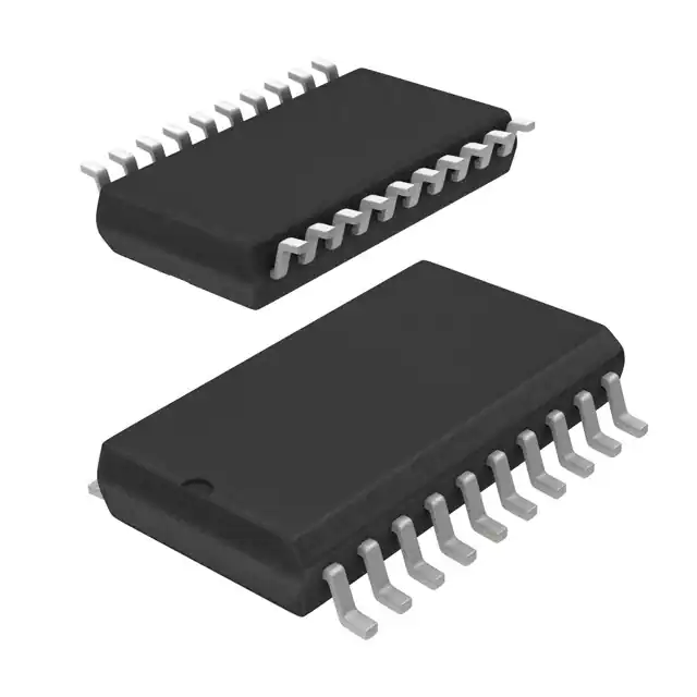
1ED020I12FA2
Single IGBT Driver IC
SP001080574
1
Overview
Main Features
•
Single channel isolated IGBT Driver
•
For 600V/1200V IGBTs
•
2 A rail-to-rail output
•
Vcesat-detection
•
Active Miller Clamp
Product Highlights
•
Coreless transformer isolated driver
•
Basic insulation according to DIN EN 60747-5-2
•
Basic insulation recognized under UL 1577
•
Integrated protection features
•
Suitable for operation at high ambient temperature
•
AEC Qualified
Typical Application
•
Drive inverters for HEV and EV
•
Auxiliary inverters for HEV and EV
•
High Power DC/DC inverters
Description
The 1ED020I12FA2 is a galvanic isolated single channel IGBT driver in PG-DSO-20 package that provides an
output current capability of typically 2A.
All logic pins are 5V CMOS compatible and could be directly connected to a microcontroller.
The data transfer across galvanic isolation is realized by the integrated Coreless Transformer Technology.
The 1ED020I12FA2 provides several protection features like IGBT desaturation protection, active Miller clamping
and active shut down.
Type
Package
Marking
1ED020I12FA2
PG-DSO-20
1ED020I12FA2
Data Sheet
www.infineon.com
1
Rev. 3.0
2016-04-04
�1ED020I12FA2
Single IGBT Driver IC
Table of Contents
1
Overview . . . . . . . . . . . . . . . . . . . . . . . . . . . . . . . . . . . . . . . . . . . . . . . . . . . . . . . . . . . . . . . . . . . . . . . 1
Table of Contents . . . . . . . . . . . . . . . . . . . . . . . . . . . . . . . . . . . . . . . . . . . . . . . . . . . . . . . . . . . . . . . . 2
List of Figures . . . . . . . . . . . . . . . . . . . . . . . . . . . . . . . . . . . . . . . . . . . . . . . . . . . . . . . . . . . . . . . . . . . 3
List of Tables . . . . . . . . . . . . . . . . . . . . . . . . . . . . . . . . . . . . . . . . . . . . . . . . . . . . . . . . . . . . . . . . . . . . 4
2
Block Diagram . . . . . . . . . . . . . . . . . . . . . . . . . . . . . . . . . . . . . . . . . . . . . . . . . . . . . . . . . . . . . . . . . . . 5
3
3.1
3.2
Pin Configuration and Functionality . . . . . . . . . . . . . . . . . . . . . . . . . . . . . . . . . . . . . . . . . . . . . . . . . 6
Pin Configuration . . . . . . . . . . . . . . . . . . . . . . . . . . . . . . . . . . . . . . . . . . . . . . . . . . . . . . . . . . . . . . . . . 6
Pin Functionality . . . . . . . . . . . . . . . . . . . . . . . . . . . . . . . . . . . . . . . . . . . . . . . . . . . . . . . . . . . . . . . . . . 7
4
4.1
4.2
4.3
4.3.1
4.3.2
4.3.3
4.3.4
4.4
4.5
4.6
4.6.1
4.6.2
4.6.3
4.7
Functional Description . . . . . . . . . . . . . . . . . . . . . . . . . . . . . . . . . . . . . . . . . . . . . . . . . . . . . . . . . . . . 9
Introduction . . . . . . . . . . . . . . . . . . . . . . . . . . . . . . . . . . . . . . . . . . . . . . . . . . . . . . . . . . . . . . . . . . . . . . 9
Supply . . . . . . . . . . . . . . . . . . . . . . . . . . . . . . . . . . . . . . . . . . . . . . . . . . . . . . . . . . . . . . . . . . . . . . . . . . 9
Internal Protection Features . . . . . . . . . . . . . . . . . . . . . . . . . . . . . . . . . . . . . . . . . . . . . . . . . . . . . . . . 10
Undervoltage Lockout (UVLO) . . . . . . . . . . . . . . . . . . . . . . . . . . . . . . . . . . . . . . . . . . . . . . . . . . . . . 10
READY Status Output . . . . . . . . . . . . . . . . . . . . . . . . . . . . . . . . . . . . . . . . . . . . . . . . . . . . . . . . . . . 10
Watchdog Timer . . . . . . . . . . . . . . . . . . . . . . . . . . . . . . . . . . . . . . . . . . . . . . . . . . . . . . . . . . . . . . . 10
Active Shut-Down . . . . . . . . . . . . . . . . . . . . . . . . . . . . . . . . . . . . . . . . . . . . . . . . . . . . . . . . . . . . . . 11
Non-Inverting and Inverting Inputs . . . . . . . . . . . . . . . . . . . . . . . . . . . . . . . . . . . . . . . . . . . . . . . . . . . 11
Driver Output . . . . . . . . . . . . . . . . . . . . . . . . . . . . . . . . . . . . . . . . . . . . . . . . . . . . . . . . . . . . . . . . . . . 11
External Protection Features . . . . . . . . . . . . . . . . . . . . . . . . . . . . . . . . . . . . . . . . . . . . . . . . . . . . . . . 11
Desaturation Protection . . . . . . . . . . . . . . . . . . . . . . . . . . . . . . . . . . . . . . . . . . . . . . . . . . . . . . . . . . 11
Active Miller Clamp . . . . . . . . . . . . . . . . . . . . . . . . . . . . . . . . . . . . . . . . . . . . . . . . . . . . . . . . . . . . . 11
Short Circuit Clamping . . . . . . . . . . . . . . . . . . . . . . . . . . . . . . . . . . . . . . . . . . . . . . . . . . . . . . . . . . . 11
RESET . . . . . . . . . . . . . . . . . . . . . . . . . . . . . . . . . . . . . . . . . . . . . . . . . . . . . . . . . . . . . . . . . . . . . . . . 11
5
5.1
5.2
5.3
5.4
5.4.1
5.4.2
5.4.3
5.4.4
5.4.5
5.4.6
5.4.7
5.4.8
Electrical Parameters . . . . . . . . . . . . . . . . . . . . . . . . . . . . . . . . . . . . . . . . . . . . . . . . . . . . . . . . . . . .
Absolute Maximum Ratings . . . . . . . . . . . . . . . . . . . . . . . . . . . . . . . . . . . . . . . . . . . . . . . . . . . . . . . .
Operating Parameters . . . . . . . . . . . . . . . . . . . . . . . . . . . . . . . . . . . . . . . . . . . . . . . . . . . . . . . . . . . .
Recommended Operating Parameters . . . . . . . . . . . . . . . . . . . . . . . . . . . . . . . . . . . . . . . . . . . . . . . .
Electrical Characteristics . . . . . . . . . . . . . . . . . . . . . . . . . . . . . . . . . . . . . . . . . . . . . . . . . . . . . . . . . .
Voltage Supply . . . . . . . . . . . . . . . . . . . . . . . . . . . . . . . . . . . . . . . . . . . . . . . . . . . . . . . . . . . . . . . . .
Logic Input and Output . . . . . . . . . . . . . . . . . . . . . . . . . . . . . . . . . . . . . . . . . . . . . . . . . . . . . . . . . .
Gate Driver . . . . . . . . . . . . . . . . . . . . . . . . . . . . . . . . . . . . . . . . . . . . . . . . . . . . . . . . . . . . . . . . . . .
Active Miller Clamp . . . . . . . . . . . . . . . . . . . . . . . . . . . . . . . . . . . . . . . . . . . . . . . . . . . . . . . . . . . . .
Short Circuit Clamping . . . . . . . . . . . . . . . . . . . . . . . . . . . . . . . . . . . . . . . . . . . . . . . . . . . . . . . . . . .
Dynamic Characteristics . . . . . . . . . . . . . . . . . . . . . . . . . . . . . . . . . . . . . . . . . . . . . . . . . . . . . . . . .
Desaturation Protection . . . . . . . . . . . . . . . . . . . . . . . . . . . . . . . . . . . . . . . . . . . . . . . . . . . . . . . . . .
Active Shut Down . . . . . . . . . . . . . . . . . . . . . . . . . . . . . . . . . . . . . . . . . . . . . . . . . . . . . . . . . . . . . .
12
12
13
13
14
14
15
16
16
17
17
18
20
6
6.1
6.2
6.3
Insulation Characteristics . . . . . . . . . . . . . . . . . . . . . . . . . . . . . . . . . . . . . . . . . . . . . . . . . . . . . . . .
Certified according to DIN EN 60747-5-2 (VDE 0884 Teil 2): 2003-01. Basic Insulation . . . . . . . . . .
Recognized under UL 1577 . . . . . . . . . . . . . . . . . . . . . . . . . . . . . . . . . . . . . . . . . . . . . . . . . . . . . . . .
Reliability . . . . . . . . . . . . . . . . . . . . . . . . . . . . . . . . . . . . . . . . . . . . . . . . . . . . . . . . . . . . . . . . . . . . . .
21
21
21
21
7
Timing Diagramms . . . . . . . . . . . . . . . . . . . . . . . . . . . . . . . . . . . . . . . . . . . . . . . . . . . . . . . . . . . . . . 22
8
Package Outlines . . . . . . . . . . . . . . . . . . . . . . . . . . . . . . . . . . . . . . . . . . . . . . . . . . . . . . . . . . . . . . . 24
9
9.1
9.2
Application Notes . . . . . . . . . . . . . . . . . . . . . . . . . . . . . . . . . . . . . . . . . . . . . . . . . . . . . . . . . . . . . . . 25
Reference Layout for Thermal Data . . . . . . . . . . . . . . . . . . . . . . . . . . . . . . . . . . . . . . . . . . . . . . . . . . 25
Printed Circuit Board Guidelines . . . . . . . . . . . . . . . . . . . . . . . . . . . . . . . . . . . . . . . . . . . . . . . . . . . . . 25
Data Sheet
2
Rev. 3.0
2016-04-04
�1ED020I12FA2
Single IGBT Driver IC
List of Figures
Figure 1
Figure 2
Figure 3
Figure 4
Figure 5
Figure 6
Figure 7
Figure 8
Figure 9
Figure 10
Data Sheet
Block Diagram 1ED020I12FA2. . . . . . . . . . . . . . . . . . . . . . . . . . . . . . . . . . . . . . . . . . . . . . . . . . . . . 5
PG-DSO-20 (top view) . . . . . . . . . . . . . . . . . . . . . . . . . . . . . . . . . . . . . . . . . . . . . . . . . . . . . . . . . . . 7
Application Example Bipolar Supply . . . . . . . . . . . . . . . . . . . . . . . . . . . . . . . . . . . . . . . . . . . . . . . . . 9
Application Example Unipolar Supply. . . . . . . . . . . . . . . . . . . . . . . . . . . . . . . . . . . . . . . . . . . . . . . 10
Propagation Delay, Rise and Fall Time . . . . . . . . . . . . . . . . . . . . . . . . . . . . . . . . . . . . . . . . . . . . . 22
Typical Switching Behavior. . . . . . . . . . . . . . . . . . . . . . . . . . . . . . . . . . . . . . . . . . . . . . . . . . . . . . . 22
DESAT Switch-Off Behavior . . . . . . . . . . . . . . . . . . . . . . . . . . . . . . . . . . . . . . . . . . . . . . . . . . . . . . 23
UVLO Behavior. . . . . . . . . . . . . . . . . . . . . . . . . . . . . . . . . . . . . . . . . . . . . . . . . . . . . . . . . . . . . . . . 23
PG-DSO-20 (Plastic (Green) Dual Small Outline Package) . . . . . . . . . . . . . . . . . . . . . . . . . . . . . . 24
Reference Layout for Thermal Data (Copper thickness 102 μm) . . . . . . . . . . . . . . . . . . . . . . . . . . 25
3
Rev. 3.0
2016-04-04
�1ED020I12FA2
Single IGBT Driver IC
List of Tables
Table 1
Table 2
Table 3
Table 4
Table 5
Table 6
Table 7
Table 8
Table 9
Table 10
Table 11
Table 12
Table 13
Table 14
Data Sheet
Pin Configuration . . . . . . . . . . . . . . . . . . . . . . . . . . . . . . . . . . . . . . . . . . . . . . . . . . . . . . . . . . . . . . . 6
Absolute Maximum Ratings . . . . . . . . . . . . . . . . . . . . . . . . . . . . . . . . . . . . . . . . . . . . . . . . . . . . . . 12
Operating Parameters . . . . . . . . . . . . . . . . . . . . . . . . . . . . . . . . . . . . . . . . . . . . . . . . . . . . . . . . . . 13
Recommended Operating Parameters . . . . . . . . . . . . . . . . . . . . . . . . . . . . . . . . . . . . . . . . . . . . . 13
Voltage Supply . . . . . . . . . . . . . . . . . . . . . . . . . . . . . . . . . . . . . . . . . . . . . . . . . . . . . . . . . . . . . . . . 14
Logic Input and Output . . . . . . . . . . . . . . . . . . . . . . . . . . . . . . . . . . . . . . . . . . . . . . . . . . . . . . . . . 15
Gate Driver . . . . . . . . . . . . . . . . . . . . . . . . . . . . . . . . . . . . . . . . . . . . . . . . . . . . . . . . . . . . . . . . . . 16
Active Miller Clamp . . . . . . . . . . . . . . . . . . . . . . . . . . . . . . . . . . . . . . . . . . . . . . . . . . . . . . . . . . . . 16
Short Circuit Clamping . . . . . . . . . . . . . . . . . . . . . . . . . . . . . . . . . . . . . . . . . . . . . . . . . . . . . . . . . . 17
Dynamic Characteristics . . . . . . . . . . . . . . . . . . . . . . . . . . . . . . . . . . . . . . . . . . . . . . . . . . . . . . . . 17
Desaturation Protection . . . . . . . . . . . . . . . . . . . . . . . . . . . . . . . . . . . . . . . . . . . . . . . . . . . . . . . . . 18
Active Shut Down . . . . . . . . . . . . . . . . . . . . . . . . . . . . . . . . . . . . . . . . . . . . . . . . . . . . . . . . . . . . . 20
According to DIN EN 60747-5-2 . . . . . . . . . . . . . . . . . . . . . . . . . . . . . . . . . . . . . . . . . . . . . . . . . . 21
Recognized under UL 1577 . . . . . . . . . . . . . . . . . . . . . . . . . . . . . . . . . . . . . . . . . . . . . . . . . . . . . . 21
4
Rev. 3.0
2016-04-04
�1ED020I12FA2
Single IGBT Driver IC
Block Diagram
2
Block Diagram
VCC1
18
UVLO
UVLO
&
IN+
13
K4
TX
VCC2
8
CLAMP
7
OUT
5
NC
3
DESAT
4
GND2
2V
delay
delay
6
&
RX
1
VCC1
IN-
VCC2
14
&
VCC1
RDY
VEE2
15
FLT2
&
/RDY
1
DECODER
RX
TX
ENCODER
VEE2
VCC2
VCC1
16
FLT
1
RDY2
FLTNL
/FLT
&
&
≥1
S
17
9V
Q
R
≥1
VCC1
/RST
I3
K3
delay
RST
1
2
VEE2
Figure 1
Data Sheet
11
12
GND1
GND1
1
19
GND1
20
1ED020 I12FA2
GND1
1
2
9
10
VEE2
VEE2
VEE2
VEE2
Block Diagram 1ED020I12FA2
5
Rev. 3.0
2016-04-04
�1ED020I12FA2
Single IGBT Driver IC
Pin Configuration and Functionality
3
Pin Configuration and Functionality
3.1
Pin Configuration
Table 1
Pin Configuration
Pin No. Name
Function
1
VEE2
Negative power supply output side
2
VEE2
Negative power supply output side
3
DESAT
Desaturation protection
4
GND2
Signal ground output side
5
NC
Not connected
6
VCC2
Positive power supply output side
7
OUT
Driver output
8
CLAMP
Miller clamping
9
VEE2
Negative power supply output side
10
VEE2
Negative power supply output side
11
GND1
Ground input side
12
GND1
Ground input side
13
IN+
Non inverted driver input
14
IN-
Inverted driver input
15
RDY
Ready output
16
/FLT
Fault output, low active
17
/RST
Reset input, low active
18
VCC1
Positive power supply input side
19
GND1
Ground input side
20
GND1
Ground input side
Data Sheet
6
Rev. 3.0
2016-04-04
�1ED020I12FA2
Single IGBT Driver IC
Pin Configuration and Functionality
Figure 2
PG-DSO-20 (top view)
3.2
Pin Functionality
1
VEE2
GND1 20
2
VEE2
GND1 19
3
DESAT
VCC1 18
4
GND2
/RST 17
5
NC
/FLT 16
6
VCC2
RDY 15
7
OUT
IN- 14
8
CLAMP
IN+ 13
9
VEE2
GND1 12
10
VEE2
GND1 11
GND1
Ground connection of the input side.
IN+ Non Inverting Driver Input
IN+ control signal for the driver output if IN- is set to low. (The IGBT is on if IN+ = high and IN- = low)
A minimum pulse width is defined to make the IC robust against glitches at IN+. An internal Pull-Down-Resistor
ensures IGBT Off-State.
IN- Inverting Driver Input
IN- control signal for driver output if IN+ is set to high. (IGBT is on if IN- = low and IN+ = high)
A minimum pulse width is defined to make the IC robust against glitches at IN-. An internal Pull-Up-Resistor
ensures IGBT Off-State.
/RST Reset Input
Function 1: Enable/shutdown of the input chip. (The IGBT is off if /RST = low). A minimum pulse width is
defined to make the IC robust against glitches at /RST.
Function 2: Resets the DESAT-FAULT-state of the chip if /RST is low for a time TRST. An internal Pull-Up-Resistor
is used to ensure /FLT status output.
/FLT Fault Output
Open-drain output to report a desaturation error of the IGBT (FLT is low if desaturation occurs)
Data Sheet
7
Rev. 3.0
2016-04-04
�1ED020I12FA2
Single IGBT Driver IC
Pin Configuration and Functionality
RDY Ready Status
Open-drain output to report the correct operation of the device (RDY = high if both chips are above the UVLO
level and the internal chip transmission is faultless).
VCC1
5 V power supply of the input chip
VEE2
Negative power supply pins of the output chip. If no negative supply voltage is available, all VEE2 pins have to
be connected to GND2.
DESAT Desaturation Detection Input
Monitoring of the IGBT saturation voltage (VCE) to detect desaturation caused by short circuits. If OUT is high,
VCE is above a defined value and a certain blanking time has expired, the desaturation protection is activated
and the IGBT is switched off. The blanking time is adjustable by an external capacitor.
CLAMP Miller Clamping
Ties the gate voltage to ground after the IGBT has been switched off at a defined voltage to avoid a parasitic
switch-on of the IGBT.During turn-off, the gate voltage is monitored and the clamp output is activated when
the gate voltage goes below 2 V below VEE2.
GND2 Reference Ground
Reference ground of the output chip.
OUT Driver Output
Output pin to drive an IGBT. The voltage is switched between VEE2 and VCC2. In normal operating mode Vout
is controlled by IN+, IN- and /RST. During error mode (UVLO, internal error or DESAT) Vout is set to VEE2
independent of the input control signals.
VCC2
Positive power supply pin of the output side.
Data Sheet
8
Rev. 3.0
2016-04-04
�1ED020I12FA2
Single IGBT Driver IC
Functional Description
4
Functional Description
4.1
Introduction
The 1ED020I12FA2 is an advanced IGBT gate driver that can be also used for driving power MOS devices.
Control and protection functions are included to make possible the design of high reliability systems.
The device consists of two galvanic separated parts. The input chip can be directly connected to a standard
5 V DSP or microcontroller with CMOS in/output and the output chip is connected to the high voltage side.
The rail-to-rail driver output enables the user to provide easy clamping of the IGBTs gate voltage during short
circuit of the IGBT. So an increase of short circuit current due to the feedback via the Miller capacitance can be
avoided. Further, a rail-to-rail output reduces power dissipation.
The device also includes IGBT desaturation protection with FAULT status output.
The READY status output reports if the device is supplied and operates correctly.
+5V
10k
10k
VCC1
SGND
100n
1µ
CLAMP
OUT
IN+
RDY
FLT
/RST
Figure 3
Application Example Bipolar Supply
4.2
Supply
220p
GND2
/FLT
RST
10R
NC
IN-
RDY
1k
DESAT
GND1
IN+
+15V
VCC2
1µ
VEE2
-8V
The driver 1ED020I12FA2 is designed to support two different supply configurations, bipolar supply and
unipolar supply.
In bipolar supply the driver is typically supplied with a positive voltage of 15V at VCC2 and a negative voltage
of -8V at VEE2, please refer to Figure 3. Negative supply prevents a dynamic turn on due to the additional
charge which is generated from IGBT input capacitance times negative supply voltage. If an appropriate
negative supply voltage is used, connecting CLAMP to IGBT gate is redundant and therefore typically not
necessary.
For unipolar supply configuration the driver is typically supplied with a positive voltage of 15V at VCC2.
Erratically dynamic turn on of the IGBT could be prevented with active Miller clamp function, so CLAMP output
is directly connected to IGBT gate, please refer to Figure 4.
Data Sheet
9
Rev. 3.0
2016-04-04
�1ED020I12FA2
Single IGBT Driver IC
Functional Description
10R
10k
10k
+5V
VCC1
1µ
100n
SGND
+15V
VCC2
1k
DESAT
GND1
CLAMP
10R
IN+
IN+
OUT
NC
IN-
RDY
RDY
FLT
220p
GND2
/FLT
RST
/RST
Figure 4
Application Example Unipolar Supply
4.3
Internal Protection Features
4.3.1
Undervoltage Lockout (UVLO)
VEE2
To ensure correct switching of IGBTs the device is equipped with an undervoltage lockout for both chips, refer
to Figure 8.
If the power supply voltage VVCC1 of the input chip drops below VUVLOL1 a turn-off signal is sent to the output
chip before power-down. The IGBT is switched off and the signals at IN+ and IN- are ignored as long as VVCC1
reaches the power-up voltage VUVLOH1.
If the power supply voltage VVCC2 of the output chip goes down below VUVLOL2 the IGBT is switched off and
signals from the input chip are ignored as long as VVCC2 reaches the power-up voltage VUVLOH2. VEE2 is not
monitored, otherwise negative supply voltage range from 0 V to -12 V would not be possible.
4.3.2
READY Status Output
The READY output shows the status of three internal protection features.
•
•
•
UVLO of the input chip
UVLO of the output chip after a short delay
Internal signal transmission after a short delay
It is not necessary to reset the READY signal since its state only depends on the status of the former mentioned
protection signals.
4.3.3
Watchdog Timer
During normal operation the internal signal transmission is monitored by a watchdog timer. If the
transmission fails for a given time, the IGBT is switched off and the READY output reports an internal error.
Data Sheet
10
Rev. 3.0
2016-04-04
�1ED020I12FA2
Single IGBT Driver IC
Functional Description
4.3.4
Active Shut-Down
The Active Shut-Down feature ensures a safe IGBT off-state if the output chip is not connected to the power
supply, IGBT gate is clamped at OUT to VEE2.
4.4
Non-Inverting and Inverting Inputs
There are two possible input modes to control the IGBT. At non-inverting mode IN+ controls the driver output
while IN- is set to low. At inverting mode IN- controls the driver output while IN+ is set to high, please see
Figure 6. A minimum input pulse width is defined to filter occasional glitches.
4.5
Driver Output
The output driver sections uses only MOSFETs to provide a rail-to-rail output. This feature permits that tight
control of gate voltage during on-state and short circuit can be maintained as long as the drivers supply is
stable. Due to the low internal voltage drop, switching behaviour of the IGBT is predominantly governed by
the gate resistor. Furthermore, it reduces the power to be dissipated by the driver.
4.6
External Protection Features
4.6.1
Desaturation Protection
A desaturation protection ensures the protection of the IGBT at short circuit. When the DESAT voltage goes up
and reaches 9 V, the output is driven low. Further, the FAULT output is activated, please refer to Figure 7. A
programmable blanking time is used to allow enough time for IGBT saturation. Blanking time is provided by a
highly precise internal current source and an external capacitor.
4.6.2
Active Miller Clamp
In a half bridge configuration the switched off IGBT tends to dynamically turn on during turn on phase of the
opposite IGBT. A Miller clamp allows sinking the Miller current across a low impedance path in this high dV/dt
situation. Therefore in many applications, the use of a negative supply voltage can be avoided.
During turn-off, the gate voltage is monitored and the clamp output is activated when the gate voltage goes
below typical 2 V (related to VEE2). The clamp is designed for a Miller current up to 2 A.
4.6.3
Short Circuit Clamping
During short circuit the IGBTs gate voltage tends to rise because of the feedback via the Miller capacitance. An
additional protection circuit connected to OUT and CLAMP limits this voltage to a value slightly higher than
the supply voltage. A current of maximum 500 mA for 10 μs may be fed back to the supply through one of this
paths. If higher currents are expected or a tighter clamping is desired external Schottky diodes may be added.
4.7
RESET
The reset inputs have two functions.
Firstly, /RST is in charge of setting back the FAULT output. If /RST is low longer than a given time, /FLT will be
cleared at the rising edge of /RST, refer to Figure 7; otherwise, it will remain unchanged. Moreover, it works as
enable/shutdown of the input logic, refer to Figure 6.
Data Sheet
11
Rev. 3.0
2016-04-04
�1ED020I12FA2
Single IGBT Driver IC
Electrical Parameters
5
Electrical Parameters
5.1
Absolute Maximum Ratings
Note:
Absolute maximum ratings are defined as ratings, which when being exceeded may lead to
destruction of the integrated circuit. Unless otherwise noted all parameters refer to GND1.
Table 2
Absolute Maximum Ratings
Parameter
Symbol
Values
Min.
Max.
Unit
Note
Positive power supply output side
VVCC2
-0.3
20
V
1)
Negative power supply output side
VVEE2
-12
0.3
V
1)
Maximum power supply voltage output side
(VVCC2 - VVEE2)
Vmax2
–
28
V
–
Gate driver output
VOUT
VVEE2-0.3
VVCC2+0.3 V
–
Gate driver high output maximum current
IOUT
–
2.4
A
t = 2 µs
Gate & Clamp driver low output maximum
current
IOUT
–
2.4
A
t = 2 µs
Maximum short circuit clamping time
tCLP
–
10
μs
ICLAMP/OUT =
500 mA
Positive power supply input side
VVCC1
-0.3
6.5
V
–
Logic input voltages
(IN+,IN-,RST)
VLogicIN
-0.3
6.5
V
–
Opendrain Logic output voltage (FLT)
VFLT#
-0.3
6.5
V
–
Opendrain Logic output voltage (RDY)
VRDY
-0.3
6.5
V
–
Opendrain Logic output current (FLT)
IFLT#
–
10
mA
–
Opendrain Logic output current (RDY)
IRDY
–
10
mA
–
Pin DESAT voltage
VDESAT
-0.3
VVCC2 +0.3 V
1)
Pin CLAMP voltage
VCLAMP
-0.3
VVCC2
+0.32)
V
3)
Junction temperature
TJ
-40
150
°C
–
Storage temperature
TS
-55
150
°C
–
Power dissipation, per input part
PD, IN
–
100
mW
4)
@TA = 25°C
Power dissipation, per output part
PD, OUT
–
700
mW
4)
@TA = 25°C
K/W
4)
@TA = 25°C
@TA = 25°C
Thermal resistance (Input part)
RTHJA,IN
–
139
Thermal resistance (Output chip active)
RTHJA,OUT
–
117
K/W
4)
ESD Capability
VESD
–
1
kV
Human Body
Model5)
1) With respect to GND2.
2) May be exceeded during short circuit clamping.
Data Sheet
12
Rev. 3.0
2016-04-04
�1ED020I12FA2
Single IGBT Driver IC
Electrical Parameters
3) With respect to VEE2.
4) Output IC power dissipation is derated linearly at 8.5 mW/°C above 68°C. Input IC power dissipation does not require
derating. See Figure 10 for reference layouts for these thermal data. Thermal performance may change significantly
with layout and heat dissipation of components in close proximity.
5) According to EIA/JESD22-A114-B (discharging a 100 pF capacitor through a 1.5 kΩ series resistor).
5.2
Operating Parameters
Note:
Within the operating range the IC operates as described in the functional description. Unless
otherwise noted all parameters refer to GND1.
Table 3
Operating Parameters
Parameter
Symbol
Values
Min.
Max.
Unit
Note
Positive power supply output side
VVCC2
13
20
V
1)
Negative power supply output side
VVEE2
-12
0
V
1)
Maximum power supply voltage
output side
(VVCC2 - VVEE2)
Vmax2
–
28
V
–
Positive power supply input side
VVCC1
4.5
5.5
V
–
Logic input voltages
(IN+,IN-,RST)
VLogicIN
-0.3
5.5
V
–
Pin CLAMP voltage
VCLAMP
VVEE2-0.3
VVCC22)
V
–
Pin DESAT voltage
VDESAT
-0.3
VVCC2
V
1)
Pin TLSET voltage
VTLSET
-0.3
VVCC2
V
1)
Ambient temperature
TA
-40
125
°C
–
Common mode transient
immunity3)
|DVISO/dt|
–
50
kV/μs
@ 500 V
1) With respect to GND2.
2) May be exceeded during short circuit clamping.
3) The parameter is not subject to production test - verified by design/characterization
5.3
Recommended Operating Parameters
Note:
Unless otherwise noted all parameters refer to GND1.
Table 4
Recommended Operating Parameters
Parameter
Symbol
Value
Unit
Note
Positive power supply output side
VVCC2
15
V
1)
Negative power supply output side
VVEE2
-8
V
1)
Positive power supply input side
VVCC1
5
V
–
1) With respect to GND2.
Data Sheet
13
Rev. 3.0
2016-04-04
�1ED020I12FA2
Single IGBT Driver IC
Electrical Parameters
5.4
Electrical Characteristics
Note:
The electrical characteristics include the spread of values in supply voltages, load and junction
temperatures given below. Typical values represent the median values at TA = 25°C. Unless
otherwise noted all voltages are given with respect to their respective GND (GND1 for pins 9 to 16,
GND2 for pins 1 to 8).
5.4.1
Voltage Supply
Table 5
Voltage Supply
Parameter
Symbol
Values
Min.
Typ.
Max.
Unit
Note
UVLO Threshold Input
Chip
VUVLOH1
–
4.1
4.3
V
–
VUVLOL1
3.5
3.8
–
V
–
UVLO Hysteresis Input
Chip (VUVLOH1 - VUVLOL1)
VHYS1
0.15
–
–
V
–
UVLO Threshold Output VUVLOH2
Chip
VUVLOL2
–
12.0
12.6
V
–
10.4
11.0
–
V
–
UVLO Hysteresis Output VHYS2
Chip (VUVLOH1 - VUVLOL1)
0.7
0.9
–
V
–
Quiescent Current Input IQ1
Chip
–
7
9
mA
VVCC1 = 5 V
IN+ = High,
IN- = Low
=>OUT = High,
RDY = High,
/FLT = High
Quiescent Current
Output Chip
–
4
6
mA
VVCC2 = 15 V
VVEE2 = -8 V
IN+ = High,
IN- = Low
=>OUT = High,
RDY = High,
/FLT = High
Data Sheet
IQ2
14
Rev. 3.0
2016-04-04
�1ED020I12FA2
Single IGBT Driver IC
Electrical Parameters
5.4.2
Logic Input and Output
Table 6
Logic Input and Output
Parameter
Symbol
Values
Unit
Note
Min.
Typ.
Max.
IN+,IN-, RST Low Input Voltage VIN+L,
VIN-L,
VRSTL#
–
–
1.5
V
–
IN+,IN-, RST High Input Voltage VIN+H,
VIN-H,
VRSTH#
3.5
–
–
V
–
IN-, RST Input Current
IIN-, IRST#
-400
-100
–
μA
VIN- = GND1
VRST# = GND1
IN+ Input Current
IIN+,
–
100
400
μA
VIN+ = VCC1
RDY,FLT Pull Up Current
IPRDY, IPFLT#
-400
-100
–
μA
VRDY = GND1
VFLT# = GND1
Input Pulse Suppression IN+,
IN-
TMININ+,
TMININ-
30
40
–
ns
–
Input Pulse Suppression RST
for ENABLE/SHUTDOWN
TMINRST
30
40
–
ns
–
Pulse Width RST
for Reseting FLT
TRST
800
–
–
ns
–
FLT Low Voltage
VFLTL
–
–
300
mV
ISINK(FLT#) = 5 mA
RDY Low Voltage
VRDYL
–
–
300
mV
ISINK(RDY) = 5 mA
Data Sheet
15
Rev. 3.0
2016-04-04
�1ED020I12FA2
Single IGBT Driver IC
Electrical Parameters
5.4.3
Gate Driver
Table 7
Gate Driver
Parameter
Symbol
High Level Output
Voltage
Values
Unit
Note
Min.
Typ.
Max.
VOUTH1
VCC2 -1.2
VCC2 -0.8
–
V
IOUTH = -20 mA
VOUTH2
VCC2 -2.5
VCC2 -2.0
–
V
IOUTH = -200 mA
VOUTH3
VCC2 -9
VCC2 -5
–
V
IOUTH = -1 A
VCC2 -10
–
V
IOUTH = -2 A
VOUTH4
High Level Output Peak IOUTH
Current
-1.5
-2.0
–
A
IN+ = High,
IN- = Low;
OUT = High
Low Level Output
Voltage
VOUTL1
–
VVEE2 +0.04
VVEE2+0.09
V
IOUTL = 20 mA
VOUTL2
–
VVEE2 +0.3
VVEE2+0.85
V
IOUTL = 200 mA
VOUTL3
–
VVEE2 +2.1
VVEE2+5
V
IOUTL = 1 A
VOUTL4
–
VVEE2 +7
–
V
IOUTL = 2 A
1.5
2.0
–
A
IN+ = Low,
IN- = Low;
OUT = Low,
VVCC2 = 15 V,
VVEE2 = -8 V
Low Level Output Peak IOUTL
Current
5.4.4
Active Miller Clamp
Table 8
Active Miller Clamp
Parameter
Symbol
Values
Unit
Note
Min.
Typ.
Max.
VCLAMPL1
–
VVEE2+0.03
VVEE2 +0.08
V
IOUTL = 20 mA
VCLAMPL2
–
VVEE2+0.3
VVEE2 +0.8
V
IOUTL = 200 mA
VCLAMPL3
–
VVEE2+1.9
VVEE2 +4.8
V
Low Level Clamp
Current
ICLAMPL
2
–
–
A
IOUTL = 1 A
1)
Clamp Threshold
Voltage
VCLAMP
1.6
2.1
2.4
V
Related to VEE2
Low Level Clamp
Voltage
1) The parameter is not subject to production test - verified by design/characterization
Data Sheet
16
Rev. 3.0
2016-04-04
�1ED020I12FA2
Single IGBT Driver IC
Electrical Parameters
5.4.5
Short Circuit Clamping
Short circuit clamping characteristics are measured with IN+ = High, IN- = Low and OUT = High.
Table 9
Short Circuit Clamping
Parameter
Symbol
Values
Unit
Note
Min.
Typ.
Max.
Clamping voltage (OUT) VCLPout
(VOUT - VVCC2)
–
0.8
1.3
V
Ipulse test,
tCLPmax = 10 μs)
Clamping voltage
(CLAMP) (VVCLAMP-VVCC2)
VCLPclamp
–
1.3
–
V
ICLAMP = 500 mA
(pulse test,
tCLPmax = 10 μs)
Clamping voltage
(CLAMP)
VCLPclamp
–
0.7
1.1
V
ICLAMP = 20 mA
5.4.6
Dynamic Characteristics
Dynamic characteristics are measured with VVCC1 = 5 V, VVCC2 = 15 V and VVEE2 = -8 V.
Table 10
Dynamic Characteristics
Parameter
Symbol
Values
Min.
Typ.
Max.
Unit
Note
CLOAD = 100 pF
VIN+ = 50%,
VOUT=50% @ 25°C
Input IN+, IN- to output
propagation delay ON
TPDON
145
170
195
ns
Input IN+, IN- to output
propagation delay OFF
TPDOFF
145
165
190
ns
Input IN+, IN- to output TPDISTO
propagation delay
distortion (TPDOFF - TPDON)
-35
-5
25
ns
Input IN+, IN- to output
propagation delay ON
variation due to temp
TPDONt
160
190
220
ns
Input IN+, IN- to output
propagation delay OFF
variation due to temp
TPDOFFt
165
195
225
ns
Input IN+, IN- to output TPDISTOt
propagation delay
distortion (TPDOFF - TPDON)
-25
5
35
ns
Data Sheet
17
CLOAD = 100 pF
VIN+ = 50%,
VOUT = 50% @ 125°C
Rev. 3.0
2016-04-04
�1ED020I12FA2
Single IGBT Driver IC
Electrical Parameters
Table 10
Dynamic Characteristics (cont’d)
Parameter
Symbol
Values
Min.
Typ.
Max.
Unit
Note
CLOAD = 100 pF
VIN+ = 50%,
VOUT = 50% @ -40°C
Input IN+, IN- to output
propagation delay ON
variation due to temp
TPDONt
135
165
195
ns
Input IN+, IN- to output
propagation delay OFF
variation due to temp
TPDOFFt
125
155
185
ns
Input IN+, IN- to output TPDISTOt
propagation delay
distortion (TPDOFF - TPDON)
-40
-10
20
ns
Rise Time
10
30
60
ns
CLOAD = 1 nF
VL 10%, VH 90%
200
400
800
ns
CLOAD = 34 nF
VL 10%, VH 90%
10
50
90
ns
CLOAD = 1 nF
VL 10%, VH 90%
200
350
600
ns
CLOAD = 34 nF
VL 10%, VH 90%
Unit
Note
TRISE
Fall Time
TFALL
5.4.7
Desaturation Protection
Table 11
Desaturation Protection
Parameter
Symbol
Values
Min.
Typ.
Max.
Blanking Capacitor
Charge Current
IDESATC
450
500
550
μA
VVCC2 =15 V,
VVEE2=- 8 V
VDESAT = 2 V
Blanking Capacitor
Discharge Current
IDESATD
9
14
–
mA
VVCC2 =15 V,
VVEE2 = -8 V
VDESAT = 6 V
Desaturation
Reference Level
VDESAT
8.3
9
9.5
V
VVCC2 = 15 V
Desaturation Filter
Time
TDESATfilter
–
250
–
ns
VVCC2 = 15 V,
VVEE2 = -8 V
VDESAT = 9 V
Desaturation Sense to
OUT Low Delay
TDESATOUT
–
350
430
ns
VOUT = 90%
CLOAD = 1 nF
Desaturation Sense to
FLT Low Delay
TDESATFLT
–
–
2.25
μs
VFLT# = 10%;
IFLT # = 5 mA
Data Sheet
18
Rev. 3.0
2016-04-04
�1ED020I12FA2
Single IGBT Driver IC
Electrical Parameters
Table 11
Desaturation Protection (cont’d)
Parameter
Desaturation Low
Voltage
Symbol
VDESATL
Leading edge blanking TDESATleb
Data Sheet
Values
Unit
Note
Min.
Typ.
Max.
0.4
0.6
0.95
V
IN+ = Low, IN- = Low,
OUT = Low
–
400
–
ns
Not subject of
production test
19
Rev. 3.0
2016-04-04
�1ED020I12FA2
Single IGBT Driver IC
Electrical Parameters
5.4.8
Active Shut Down
Table 12
Active Shut Down
Parameter
Symbol
Active Shut Down Voltage VACTSD1)
Values
Min.
Typ.
Max.
–
–
2.0
Unit
Note
V
IOUT = -200 mA,
VCC2 open
1) With reference to VEE2
Data Sheet
20
Rev. 3.0
2016-04-04
�1ED020I12FA2
Single IGBT Driver IC
Insulation Characteristics
6
Insulation Characteristics
Insulation characteristics are guaranteed only within the safety maximum ratings which must be ensured by
protective circuits in application. Surface mount classification is class A in accordance with CECCOO802.
This coupler is suitable for “basic insulation” only within the safety ratings. Compliance with the safety ratings
shall be ensured by means of suitable protective circuits.
6.1
Certified according to DIN EN 60747-5-2 (VDE 0884 Teil 2): 2003-01. Basic Insulation
Table 13
According to DIN EN 60747-5-2
Description
Symbol
Characteristic
Unit
–
Installation classification per EN 60664-1, Table 1
for rated mains voltage ≤ 150 VRMS
for rated mains voltage ≤ 300 VRMS
for rated mains voltage ≤ 600 VRMS
I-IV
I-III
I-II
Climatic Classification
40/125/21
–
Pollution Degree (EN 60664-1)
2
–
Minimum External Clearance
CLR
8
mm
Minimum External Creepage
CPG
8
mm
Minimum Comparative Tracking Index
CTI
175
–
Maximum Repetitive Insulation Voltage
VIORM
1420
VPEAK
Highest Allowable Overvoltage
VIOTM
6000
VPEAK
Maximum Surge Insulation Voltage
VIOSM
6000
V
Description
Symbol
Characteristic
Unit
Insulation Withstand Voltage / 1 min
VISO
3750
Vrms
Insulation Test Voltage / 1 s
VISO
4500
Vrms
6.2
Recognized under UL 1577
Table 14
Recognized under UL 1577
6.3
Reliability
For Qualification Report please contact your local Infineon Technologies office.
Data Sheet
21
Rev. 3.0
2016-04-04
�1ED020I12FA2
Single IGBT Driver IC
Timing Diagramms
7
Timing Diagramms
50%
IN+
90%
50%
10%
OUT
TPDON
Figure 5
TRISE
TPDOFF
TFALL
Propagation Delay, Rise and Fall Time
IN+
IN/RST
OUT
Figure 6
Data Sheet
Typical Switching Behavior
22
Rev. 3.0
2016-04-04
�1ED020I12FA2
Single IGBT Driver IC
Timing Diagramms
IN+
TPDON
TPDON
OUT
TPDOFF
TDESATfilter
TDESATOUT
VDESAT typ. 9V
TDESATleb
TDESATleb
DESAT
blanking time
/FLT
TDESATFLT
/RST
>TRSTmin
Figure 7
DESAT Switch-Off Behavior
ESD diode conduction
IN+
VUVLOH1
VUVLOL1
VCC1
VUVLOH2
VUVLOL2
VCC2
OUT
RDY
/FLT
/RST
Figure 8
Data Sheet
UVLO Behavior
23
Rev. 3.0
2016-04-04
�1ED020I12FA2
Single IGBT Driver IC
Package Outlines
8
Package Outlines
Figure 9
PG-DSO-20 (Plastic (Green) Dual Small Outline Package)
Data Sheet
24
Rev. 3.0
2016-04-04
�1ED020I12FA2
Single IGBT Driver IC
Application Notes
9
Application Notes
9.1
Reference Layout for Thermal Data
The PCB layout shown in Figure 10 represents the reference layout used for the thermal characterisation. Pins
11, 12, 19 and 20 (GND1) and pins 1, 2, 9 and 10 (VEE2) require ground plane connections for achiving
maximum power dissipation. The 1ED020I12FA2 is conceived to dissipate most of the heat generated through
this pins.
Figure 10
Reference Layout for Thermal Data (Copper thickness 102 μm)
9.2
Printed Circuit Board Guidelines
Following factors should be taken into account for an optimum PCB layout.
•
•
•
•
Sufficient spacing should be kept between high voltage isolated side and low voltage side circuits.
The same minimum distance between two adjacent high-side isolated parts of the PCB should be
maintained to increase the effective isolation and reduce parasitic coupling.
In order to ensure low supply ripple and clean switching signals, bypass capacitor trace lengths should be
kept as short as possible.
Lowest trace length for VEE2 to GND2 decoupling could be achieved with capacitor closed to pins 2 and 4.
Data Sheet
25
Rev. 3.0
2016-04-04
�1ED020I12FA2
Single IGBT Driver IC
Revision History
Page or Item
Subjects (major changes since previous revision)
Rev. 3.0, 2016-04-04
All
Update latest template
Figure 1
Blockdiagram update
Table 2,Table 3, Removed Test Condition in table header
Table 4,Table 5,
Table 6,
Table 7,
Table 8,
Table 9,
Table 10,
Table 11,
Table 12
Table 5
Changed VUVLOH1 into VUVLOL1
Table 2
Symbol changed from Vmax2 to Vcc2 in Gate driver output
Data Sheet
26
Rev. 3.0
2016-04-04
�Please read the Important Notice and Warnings at the end of this document
Trademarks of Infineon Technologies AG
µHVIC™, µIPM™, µPFC™, AU-ConvertIR™, AURIX™, C166™, CanPAK™, CIPOS™, CIPURSE™, CoolDP™, CoolGaN™, COOLiR™, CoolMOS™, CoolSET™, CoolSiC™,
DAVE™, DI-POL™, DirectFET™, DrBlade™, EasyPIM™, EconoBRIDGE™, EconoDUAL™, EconoPACK™, EconoPIM™, EiceDRIVER™, eupec™, FCOS™, GaNpowIR™,
HEXFET™, HITFET™, HybridPACK™, iMOTION™, IRAM™, ISOFACE™, IsoPACK™, LEDrivIR™, LITIX™, MIPAQ™, ModSTACK™, my-d™, NovalithIC™, OPTIGA™,
OptiMOS™, ORIGA™, PowIRaudio™, PowIRStage™, PrimePACK™, PrimeSTACK™, PROFET™, PRO-SIL™, RASIC™, REAL3™, SmartLEWIS™, SOLID FLASH™,
SPOC™, StrongIRFET™, SupIRBuck™, TEMPFET™, TRENCHSTOP™, TriCore™, UHVIC™, XHP™, XMC™.
Trademarks updated November 2015
Other Trademarks
All referenced product or service names and trademarks are the property of their respective owners.
Edition 2016-04-04
Published by
Infineon Technologies AG
81726 Munich, Germany
© 2016 Infineon Technologies AG.
All Rights Reserved.
Do you have a question about any
aspect of this document?
Email: erratum@infineon.com
IMPORTANT NOTICE
The information given in this document shall in no
event be regarded as a guarantee of conditions or
characteristics ("Beschaffenheitsgarantie").
With respect to any examples, hints or any typical
values stated herein and/or any information regarding
the application of the product, Infineon Technologies
hereby disclaims any and all warranties and liabilities
of any kind, including without limitation warranties of
non-infringement of intellectual property rights of any
third party.
In addition, any information given in this document is
subject to customer's compliance with its obligations
stated in this document and any applicable legal
requirements, norms and standards concerning
customer's products and any use of the product of
Infineon Technologies in customer's applications.
The data contained in this document is exclusively
intended for technically trained staff. It is the
responsibility of customer's technical departments to
evaluate the suitability of the product for the intended
application and the completeness of the product
information given in this document with respect to
such application.
For further information on technology, delivery terms
and conditions and prices, please contact the nearest
Infineon Technologies Office (www.infineon.com).
WARNINGS
Due to technical requirements products may contain
dangerous substances. For information on the types
in question please contact your nearest Infineon
Technologies office.
Except as otherwise explicitly approved by Infineon
Technologies in a written document signed by
authorized representatives of Infineon Technologies,
Infineon Technologies’ products may not be used in
any applications where a failure of the product or any
consequences of the use thereof can reasonably be
expected to result in personal injury.
�


 工商网监
湘ICP备2023018690号
工商网监
湘ICP备2023018690号