Data Sheet No.PD60210 Rev.D
IR3311(S)
PROGRAMMABLE CURRENT SENSING HIGH SIDE SWITCH
Product Summary
Features
•
•
•
•
•
•
•
Load current feedback
Programmable over current shutdown
Active clamp
E.S.D protection
Input referenced to Vcc
Over temperatue shutdown
Reverse battery protection
Rds(on)
12mΩ
Vcc.op.
6 to 28V
Current ratio
Ishutdown
Description
The IR 3311(S) is a Fully Protected 4 terminal high side switch.
The input signal is referenced to Vcc. When the input voltage
Vcc - Vin is higher than the specified Vih threshold, the output
power MOSFET is turned-on. When Vcc - Vin is lower than
the specified Vil threshold, the output MOSFET is turned-off.
A sense current proportional to the current in the power Mosfet
is sourced to the Ifb pin. Over-current shutdown occurs when
Vifb - Vin > 4.5 V. The current shutdown threshold is adjusted
by selecting the proper RIfb. Either over-current and over-temperature latches off the switch. The device is reset by pulling
the input pin high. Other integrated protections ( ESD, reverse
battery, active clamp ) make the IR3311(S) very rugged and
suitable for the automotive environment.
5300
6A to 58A
Active clamp
35V
Load Dump
40V
Package
5 Lead TO220
IR3311
5 Lead
D2Pak (SMD220)
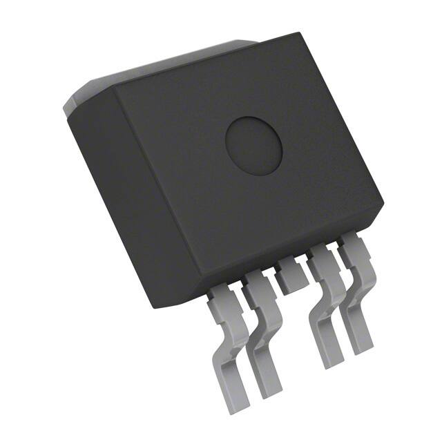
IR3311S
Typical Connection
VCC
IN
IR 3311
Ifb
Battery
OUT
10 k
LOAD
RIfb
on
off
System
Ground
Power
Ground
www.irf.com
1
�IR3311(S)
Absolute Maximum Ratings
Absolute maximum ratings indicate sustained limits beyond which damage to the device may occur. All voltage parameters
are referenced to Vcc lead. (TAmbient = 25oC unless otherwise specified).
Symbol
Parameter
Min.
Max.
Units
Vcc - Vin max
Vcc-VIfb max
-16
-0.3
-0.3
50
50
33
V
Vcc - Vout max.
Maximum input voltage
Maximum Ifb voltage
Maximum output voltage
Ids cont.
Ids1 cont
Ids pulsed
ESD 1
ESD 2
Pd
TJ max.
Diode max. permanent current (Rth = 60 °C/W) (1)
Diode max. permanent current (Rth = 5 °C/W) (1)
Diode max. pulsed current (1)
Electrostatic discharge (human body model) C=100pF, R=1500Ω,
Electrostatic discharge (machine model)C=200pF, R=0Ω, L=10µH
Power dissipation ( Rth = 60 °C/W )
Max. storage and junction temperature
—
—
—
—
—
—
-40
2.8
30
100
4
0.5
2
150
Min RIfb
Ifb max
Minimum resistor on the Ifb pin
Max. Ifb current
0.3
-20
—
+20
kΩ
mA
Typ.
Max.
Units
60
—
—
A
kV
W
°C
Thermal Characteristics
Symbol
R th
R th
R th
R th
1
2
1
2
R th 3
Parameter
Thermal resistance junction to Ambient - TO220
Thermal resistance junction to case - TO220
Thermal resistance with standard footprint - SMD220
Thermal resistance with 1" square footprint - SMD220
Thermal resistance junction to case - SMD220
0.7
60
35
0.7
—
—
—
°C/W
Recommended Operating Conditions
These values are given for a quick design. For operation outside these conditions, please consult the application notes.
Symbol
Parameter
Vcc -Vin
Vcc -VIfb
Vcc
Iout
Iout 85°C amb.
RIfb
Pulse min.
Fmax
Continuous input voltage
Continuous Ifb pin voltage
Supply to power ground voltage
Continuous output current ( Rth/amb < 5 °C/W, Tj = 125°C)
Continuous output current ( Rth/amb < 60 °C/W, Tj = 125°C)
Ifb resistor to program Isd and scale (2 & 3)
Minimum turn-on pulse width
Maximum operating frequency
Fmax Prot.
Maximum frequency with protections activated
Min.
Max.
Units
6
0.3
6
28
28
28
V
—
—
0.5
1
18
5
3.5
—
—
—
500
200
A
kΩ
ms
Hz
1) Limited by junction temperature. Pulsed current is also limited by wiring
2) 5000 Ohm or leaving Ifb open will shutdown the part. No current will flow in the load.
2
WWW.IRF.COM
�IR3311(S)
Protection Characteristics
Tj = 25oC (unless otherwise specified), RIfb = 500 to 5kOhm.
Symbol
Parameter
VIfb -Vin
@ Isd
Over-current shutdown threshold
Tsd
Treset
OV
Isdf
Isd_1k
Min.Pulse
WAIT
Over-temp. shutdown threshold
Protection reset time
Over voltage shutdown (not latched)
Fixed over current shutdown
Adjustable over current shutdown 1K
Minimum pulse width (no WAIT state)
WAIT function timer
Rev.Rdson Rds(on) reverse battery protection
Min.
Typ.
Max. Units Test Conditions
4
—
—
33
58
18
200
0.5
4.5
5.4
165
50
36
70
24
500
1.2
—
300
41
90
31
1200
3.5
µS
V
A
A
µs
ms
6
10
18
mΩ
V
°C
see Fig. 7
see Fig. 7
VIfb 60 A
Tj > 165 °C
IN
4
reverse
battery
protection
Ifb
OUT
WWW.IRF.COM
�IR3311(S)
Lead Assignments
3 (Vcc)
3 (Vcc)
1 - In
2 - Ifb
3 - Vcc (tab)
4 - NC
5 - Out
12345
12345
5 Lead - D2PAK (SMD220)
5 Lead - TO220
IR3311
IR3311S
Part Number
Vcc-Vin
Vcc-Vin
Vcc-Vin max
Vcc-Vin1 max
Vcc-Vin (op)
Vih
Vil
Vhys
Vcc-Vout
Vcc-Vout max
Vcc
Vclamp1
Vclamp2
In
IR3311
Iin
Iin
max
Iin1,2
Iin(on)
VIfb
Ifb
Out
Iout
Iout max
-Ids cont.
-Ids pulsed
Iout 85°C
Isd
Iq
Ifb
Figure 1 - Voltages and currents definitions
WWW.IRF.COM
Vcc
90%
Vcc-Vout
DV/dt(on)
5V
10 %
Td on
Tr1
Tr2
Figure 2 - Switching time definitions (turn-on)
5
�IR3311(S)
Vcc
Vcc-Vin
Vin
90%
Ids
Vcc-Vout
DV/dt(off)
T clamp
Vcc
Vds clamp
10 %
Td off
Tf
Vout
Vcc-Vclamp
( see Design tip to evaluate power dissipation )
Figure 3 - Switching time definitions (turn-off)
Vin
Figure 4 - Active clamp waveforms
clamp
Vcc-Vin
12V
0V
I Load
38 us (typ.)
T minpulse
Iout
T minpulse
Wait
Ifb
0V
Precise measurement
Figure 6 - Minimum pulse & WAIT
function
Figure 5 - Current sense precision:
Accurate measurement only when the power Mosfet is fully ON
6
WWW.IRF.COM
�IR3311(S)
Vcc-Vin
12V
0V
Iout
t < T reset
t > T reset
t > T reset
t < T reset
OI shutdown
Isd
wait
wait
Tj
OT shutdown
Tjsd
Figure 7 - Protection Timing Diagrams
All curves are typical characteristics. Operation in hatched areas is not recommended. Tj=250C, RIfb=500 Ohm,
Vcc=14V (unless otherwise specified).
16
10
14
8
12
10
6
8
4
6
4
2
2
0
0
0
10
20
30
40
50
60
Figure 8 - Icc (mA) vs Vcc-Vin (V)
WWW.IRF.COM
70
0
5
10
15
20
25
30
Figure 9- Rdson (mΩ) vs Vcc-Vin (V)
7
�IR3311(S)
200%
6
180%
5
160%
140%
4
120%
100%
3
80%
2
60%
40%
Vifb-Vin
Vih
1
20%
Vil
0%
-50 -25
0
25
50
75 100 125 150
0
-50
Figure 10 -Normalized Rdson (%) vs Tj (oC)
-25
0
25
50
125 150
Isd min 3s
isd typ
Isd max 3s
8
Max. specified
7
100
Figure 11 - Vih, Vil & Vifb -Vin (V) vs Tj (oC)
100
9
75
6
5
4
10
Typical value
3
2
1
0
0
15
30
45
60
Figure 12 - Error (+/-A) vs Iload (A)
8
1
100
1000
10000
Figure 13 - Isd (A) vs RIfb (Ohm)
WWW.IRF.COM
�IR3311(S)
5°C/W
15°C/W
35°C/W 1'' f oot
60°C/W s td f ooprint
50
45
40
100
35
30
25
10
20
15
10
single pulse
10 Hz rth=60°C/W dT=25°C
100Hz rth=60°C/W dT=25°C
1kHz rth=60°C/W dT=25°C
5
0
-50
0
50
100
150
200
1
0.001
Figure 14 - Max. DC current (A) vs Temp. (°C)
100
0.01
0.1
1
10
Figure 15 - Max. I (A) vs inductance (mH)
100
60°C/W free air
5°C/W
C urre nt path capability
should be above those
10
10
Loaad C haracte ristic
should be above those
curve s
1
T=25°C free air/ std. footprint
T=100°C free air/ std. footprint
1
0.00001 0.0001
0.1
0.001
0.01
0.1
1
10
100
1000
Figure 16 - I out (A) vs Protection resp. Time (s)
WWW.IRF.COM
0.0001
0.001
0.01
0.1
1
10
100
1000
Figure 17 - Rth (oC/W) vs Time (s)
9
�IR3311(S)
Case Outline - TO220 (5 lead)
IRGB 01-3042 01
10
WWW.IRF.COM
�IR3311(S)
Case Outline 5 Lead - D2PAK (SMD220)
WWW.IRF.COM
11
�IR3311(S)
Tape & Reel
5 Lead - D2PAK (SMD220)
01-3071 00 / 01-3072 00
IR WORLD HEADQUARTERS: 233 Kansas St., El Segundo, California 90245 Tel: (310) 252-7105
Data and specifications subject to change without notice.
This product has been designed and qualified for the Automotive [Q100] market.
7/24/2004
12
WWW.IRF.COM
�Note: For the most current drawings please refer to the IR website at:
http://www.irf.com/package/
�
很抱歉,暂时无法提供与“98-0383”相匹配的价格&库存,您可以联系我们找货
免费人工找货