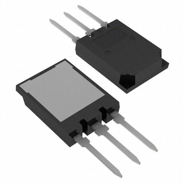
AIKQ100N60CT
TRENCHSTOPTM�Series
Low�Loss�DuoPack:�IGBT�in�TRENCHSTOPTM�and�Fieldstop�technology
with�soft,�fast�recovery�antiparallel�Emitter�Controlled�diode
�
Features:
C
•��Automotive�AEC-Q101�qualified
•��Designed�for�DC/AC�converters�for�Automotive�Application
•��Very�low��VCE(sat)�1.5V�(typ.)
•��Maximum�junction�temperature�175°C
•��Dynamically�stress�tested
•��Short�circuit�withstand�time�5µs
•��100%�short�circuit�tested
•��100%�of�the�parts�are�dynamically�tested
•��Positive�temperature�coefficient�in�VCE(sat)
•��Low�EMI
•��Low�gate�charge�QG
•��Green�package
•��Very�soft,�fast�recovery�antiparallel�Emitter�Controlled�HE
���diode
•��TRENCHSTOPTM�and�Fieldstop�technology�for�600V
���applications�offers:
������-�very�tight�parameter�distribution
������-�high�ruggedness,�temperature�stable�behavior
������-�very�high�switching�speed
G
E
Applications:
•��Main�inverter
•��Climate�compressor
•��PTC�heater
•��Motor�drives
Key�Performance�and�Package�Parameters
Type
AIKQ100N60CT
Datasheet
www.infineon.com
VCE
IC
VCEsat,�Tvj=25°C
Tvjmax
Marking
Package
600V
100A
1.5V
175°C
AK100DCT
PG-TO247-3-46
Please�read�the�Important�Notice�and�Warnings�at�the�end�of�this�document
V�2.1
2017-02-09
�AIKQ100N60CT
TRENCHSTOPTM�Series
Table�of�Contents
Description . . . . . . . . . . . . . . . . . . . . . . . . . . . . . . . . . . . . . . . . . . . . . . . . . . . . . . . . . . . . . . . . . . . . . . . . 1
Table of Contents . . . . . . . . . . . . . . . . . . . . . . . . . . . . . . . . . . . . . . . . . . . . . . . . . . . . . . . . . . . . . . . . . . . 2
Maximum Ratings . . . . . . . . . . . . . . . . . . . . . . . . . . . . . . . . . . . . . . . . . . . . . . . . . . . . . . . . . . . . . . . . . . . 3
Thermal Resistance . . . . . . . . . . . . . . . . . . . . . . . . . . . . . . . . . . . . . . . . . . . . . . . . . . . . . . . . . . . . . . . . . 3
Electrical Characteristics . . . . . . . . . . . . . . . . . . . . . . . . . . . . . . . . . . . . . . . . . . . . . . . . . . . . . . . . . . . . . . 4
Electrical Characteristics Diagrams . . . . . . . . . . . . . . . . . . . . . . . . . . . . . . . . . . . . . . . . . . . . . . . . . . . . . 6
Package Drawing . . . . . . . . . . . . . . . . . . . . . . . . . . . . . . . . . . . . . . . . . . . . . . . . . . . . . . . . . . . . . . . . . . .13
Testing Conditions . . . . . . . . . . . . . . . . . . . . . . . . . . . . . . . . . . . . . . . . . . . . . . . . . . . . . . . . . . . . . . . . . .14
Revision History . . . . . . . . . . . . . . . . . . . . . . . . . . . . . . . . . . . . . . . . . . . . . . . . . . . . . . . . . . . . . . . . . . . .15
Disclaimer . . . . . . . . . . . . . . . . . . . . . . . . . . . . . . . . . . . . . . . . . . . . . . . . . . . . . . . . . . . . . . . . . . . . . . . . .16
Datasheet
2
V�2.1
2017-02-09
�AIKQ100N60CT
TRENCHSTOPTM�Series
Maximum�Ratings
Parameter
Symbol
Value
Unit
Collector-emitter�voltage,�Tvj�≥�25°C
VCE
600
V
DC�collector�current,�limited�by�Tvjmax
TC�=�25°C�value�limited�by�bondwire
TC�=�130°C
IC
160.0
100.0
A
Pulsed�collector�current,�tp�limited�by�Tvjmax
ICpuls
400.0
A
Turn off safe operating area
VCE�≤�600V,�Tvj�≤�175°C,�tp�=�1µs
-
400.0
A
Diode�forward�current,�limited�by�Tvjmax
TC�=�25°C�value�limited�by�bondwire
TC�=�117°C
IF
160.0
100.0
A
Diode�pulsed�current,�tp�limited�by�Tvjmax
IFpuls
400.0
A
Gate-emitter voltage
VGE
±20
V
Short circuit withstand time
VGE�=�15.0V,�VCC�≤�400V
Allowed number of short circuits < 1000
Time between short circuits: ≥ 1.0s
Tvj�=�150°C
tSC
Power�dissipation�TC�=�25°C
Ptot
714.0
W
Operating junction temperature
Tvj
-40...+175
°C
Storage temperature
Tstg
-55...+150
°C
µs
5
1)
Soldering temperature,
wave soldering 1.6mm (0.063in.) from case for 10s
°C
260
Thermal�Resistance
Parameter
Symbol Conditions
Value
min.
typ.
max.
Unit
Rth�Characteristics
IGBT thermal resistance,2)
junction - case
Rth(j-c)
-
-
0.21
K/W
Diode thermal resistance,2)
junction - case
Rth(j-c)
-
-
0.35
K/W
Thermal resistance
junction - ambient
Rth(j-a)
-
-
40
K/W
1)
2)
Package not recommended for surface mount application
Thermal resistance of thermal grease Rth(c-s) (case to heat sink) of more than 0.1K/W not included.
Datasheet
3
V�2.1
2017-02-09
�AIKQ100N60CT
TRENCHSTOPTM�Series
Electrical�Characteristic,�at�Tvj�=�25°C,�unless�otherwise�specified
Parameter
Symbol Conditions
Value
Unit
min.
typ.
max.
600
-
-
V
VGE�=�15.0V,�IC�=�100.0A
Tvj�=�25°C
Tvj�=�175°C
-
1.50
1.90
2.00
-
V
-
1.65
1.60
2.05
-
V
4.1
4.9
5.7
V
Static�Characteristic
Collector-emitter breakdown voltage V(BR)CES VGE�=�0V,�IC�=�0.20mA
Collector-emitter saturation voltage VCEsat
Diode forward voltage
VF
VGE�=�0V,�IF�=�100.0A
Tvj�=�25°C
Tvj�=�175°C
Gate-emitter threshold voltage
VGE(th)
IC�=�1.60mA,�VCE�=�VGE
Zero gate voltage collector current
ICES
VCE�=�600V,�VGE�=�0V
Tvj�=�25°C
Tvj�=�175°C
-
2500
40
-
µA
Gate-emitter leakage current
IGES
VCE�=�0V,�VGE�=�20V
-
-
100
nA
Transconductance
gfs
VCE�=�20V,�IC�=�100.0A
-
63.0
-
S
Integrated gate resistor
rG
Ω
none
Electrical�Characteristic,�at�Tvj�=�25°C,�unless�otherwise�specified
Parameter
Symbol Conditions
Value
Unit
min.
typ.
max.
-
6230
-
-
360
-
-
175
-
VCC�=�480V,�IC�=�100.0A,
VGE�=�15V
-
610.0
-
nC
VGE�=�15.0V,�VCC�≤�400V,
tSC�≤�5µs
Tvj�=�150°C
-
-
A
Dynamic�Characteristic
Input capacitance
Cies
Output capacitance
Coes
Reverse transfer capacitance
Cres
Gate charge
QG
Short circuit collector current
Max. 1000 short circuits
IC(SC)
Time between short circuits: ≥ 1.0s
VCE�=�25V,�VGE�=�0V,�f�=�1MHz
802
pF
Switching�Characteristic,�Inductive�Load
Parameter
Symbol Conditions
Value
Unit
min.
typ.
max.
-
30
-
ns
-
38
-
ns
-
290
-
ns
-
31
-
ns
-
3.10
-
mJ
-
2.50
-
mJ
-
5.60
-
mJ
IGBT�Characteristic,�at�Tvj�=�25°C
Turn-on delay time
td(on)
Rise time
tr
Turn-off delay time
td(off)
Fall time
tf
Turn-on energy
Eon
Turn-off energy
Eoff
Total switching energy
Ets
Datasheet
Tvj�=�25°C,
VCC�=�400V,�IC�=�100.0A,
VGE�=�0.0/15.0V,
RG(on)�=�3.6Ω,�RG(off)�=�3.6Ω,
Lσ�=�63nH,�Cσ�=�31pF
Lσ,�Cσ�from�Fig.�E
Energy losses include “tail” and
diode reverse recovery.
4
V�2.1
2017-02-09
�AIKQ100N60CT
TRENCHSTOPTM�Series
Diode�Characteristic,�at�Tvj�=�25°C
Diode reverse recovery time
trr
Diode reverse recovery charge
Qrr
Diode peak reverse recovery current Irrm
Diode peak rate of fall of reverse
recovery�current�during�tb
Tvj�=�25°C,
VR�=�400V,
IF�=�100.0A,
diF/dt�=�1100A/µs
dirr/dt
-
225
-
ns
-
2.80
-
µC
-
23.0
-
A
-
-393
-
A/µs
Switching�Characteristic,�Inductive�Load
Parameter
Symbol Conditions
Value
Unit
min.
typ.
max.
-
31
-
ns
-
52
-
ns
-
351
-
ns
-
42
-
ns
-
6.00
-
mJ
-
3.70
-
mJ
-
9.70
-
mJ
-
300
-
ns
-
8.70
-
µC
-
50.0
-
A
-
-847
-
A/µs
IGBT�Characteristic,�at�Tvj�=�175°C
Turn-on delay time
td(on)
Rise time
tr
Turn-off delay time
td(off)
Fall time
tf
Turn-on energy
Eon
Turn-off energy
Eoff
Total switching energy
Ets
Tvj�=�175°C,
VCC�=�400V,�IC�=�100.0A,
VGE�=�0.0/15.0V,
RG(on)�=�3.6Ω,�RG(off)�=�3.6Ω,
Lσ�=�63nH,�Cσ�=�31pF
Lσ,�Cσ�from�Fig.�E
Energy losses include “tail” and
diode reverse recovery.
Diode�Characteristic,�at�Tvj�=�175°C
Diode reverse recovery time
trr
Diode reverse recovery charge
Qrr
Diode peak reverse recovery current Irrm
Diode peak rate of fall of reverse
recovery�current�during�tb
Datasheet
Tvj�=�175°C,
VR�=�400V,
IF�=�100.0A,
diF/dt�=�1050A/µs
dirr/dt
5
V�2.1
2017-02-09
�AIKQ100N60CT
800
180
700
160
140
600
IC,�COLLECTOR�CURRENT�[A]
Ptot,�POWER�DISSIPATION�[W]
TRENCHSTOPTM�Series
500
400
300
200
120
100
80
60
40
100
0
20
25
50
75
100
125
150
0
175
25
50
TC,�CASE�TEMPERATURE�[°C]
Figure 1. Power�dissipation�as�a�function�of�case
temperature
(Tj≤175°C)
125
150
175
300
VGE=20V
270
VGE=20V
270
15V
13V
240
11V
210
9V
8V
180
7V
150
6V
120
90
210
7V
2.0
2.5
3.0
3.5
90
0
4.0
VCE,�COLLECTOR-EMITTER�VOLTAGE�[V]
Figure 3. Typical�output�characteristic
(Tj=25°C)
Datasheet
6V
120
30
1.5
8V
150
30
1.0
9V
180
60
0.5
13V
11V
60
0.0
15V
240
IC,�COLLECTOR�CURRENT�[A]
IC,�COLLECTOR�CURRENT�[A]
100
Figure 2. Collector�current�as�a�function�of�case
temperature
(VGE≥15V,�Tj≤175°C)
300
0
75
TC,�CASE�TEMPERATURE�[°C]
0.0
0.5
1.0
1.5
2.0
2.5
3.0
3.5
4.0
VCE,�COLLECTOR-EMITTER�VOLTAGE�[V]
Figure 4. Typical�output�characteristic
(Tj=175°C)
6
V�2.1
2017-02-09
�AIKQ100N60CT
TRENCHSTOPTM�Series
300
3.0
Tj=25°C
Tj=175°C
IC,�COLLECTOR�CURRENT�[A]
240
210
180
150
120
90
60
30
0
0
2
4
6
8
10
12
IC=38A
IC=75A
IC=100A
IC=150A
2.7
VCE(sat),�COLLECTOR-EMITTER�SATURATION�[V]
270
2.4
2.1
1.8
1.5
1.2
0.9
0.6
0.3
0.0
14
0
VGE,�GATE-EMITTER�VOLTAGE�[V]
Figure 5. Typical�transfer�characteristic
(VCE=20V)
75
100
125
150
175
1E+4
td(off)
tf
td(on)
tr
t,�SWITCHING�TIMES�[ns]
td(off)
tf
td(on)
tr
t,�SWITCHING�TIMES�[ns]
50
Figure 6. Typical�collector-emitter�saturation�voltage�as
a�function�of�junction�temperature
(VGE=15V)
1000
100
10
25
Tj,�JUNCTION�TEMPERATURE�[°C]
0
25
50
75
100
125
150
175
1000
100
10
200
IC,�COLLECTOR�CURRENT�[A]
Figure 7. Typical�switching�times�as�a�function�of
collector�current
(inductive�load,�Tj=175°C,�VCE=400V,
VGE=15/0V,�rG=3,6Ω,Dynamic�test�circuit�in
Figure E)
Datasheet
0
10
20
30
40
50
60
70
80
rG,�GATE�RESISTOR�[Ω]
Figure 8. Typical�switching�times�as�a�function�of�gate
resistor
(inductive�load,�Tj=175°C,�VCE=400V,
VGE=15/0V,�IC=100A,Dynamic�test�circuit�in
Figure E)
7
V�2.1
2017-02-09
�AIKQ100N60CT
TRENCHSTOPTM�Series
1000
7
VGE(th),�GATE-EMITTER�THRESHOLD�VOLTAGE�[V]
t,�SWITCHING�TIMES�[ns]
td(off)
tf
td(on)
tr
100
10
25
50
75
100
125
150
typ.
min.
max.
6
5
4
3
2
1
0
175
0
Tj,�JUNCTION�TEMPERATURE�[°C]
Figure 9. Typical�switching�times�as�a�function�of
junction�temperature
(inductive�load,�VCE=400V,�VGE=15/0V,
IC=100A,�rG=3,6Ω,Dynamic�test�circuit�in
Figure E)
75
100
125
150
70
Eoff
Eon
Ets
Eoff
Eon
Ets
60
E,�SWITCHING�ENERGY�LOSSES�[mJ]
25
E,�SWITCHING�ENERGY�LOSSES�[mJ]
50
Figure 10. Gate-emitter�threshold�voltage�as�a�function
of�junction�temperature
(IC=1.6mA)
30
20
15
10
50
40
30
20
5
0
25
Tj,�JUNCTION�TEMPERATURE�[°C]
10
0
25
50
75
100
125
150
175
0
200
IC,�COLLECTOR�CURRENT�[A]
Figure 11. Typical�switching�energy�losses�as�a
function�of�collector�current
(inductive�load,�Tj=175°C,�VCE=400V,
VGE=15/0V,�rG=3,6Ω,Dynamic�test�circuit�in
Figure E)
Datasheet
0
10
20
30
40
50
60
70
80
rG,�GATE�RESISTOR�[Ω]
Figure 12. Typical�switching�energy�losses�as�a
function�of�gate�resistor
(inductive�load,�Tj=175°C,�VCE=400V,
VGE=15/0V,�IC=100A,Dynamic�test�circuit�in
Figure E)
8
V�2.1
2017-02-09
�AIKQ100N60CT
TRENCHSTOPTM�Series
10
16.0
Eoff
Eon
Ets
8
7
6
5
4
3
2
12.0
10.0
8.0
6.0
4.0
2.0
1
0
Eoff
Eon
Ets
14.0
E,�SWITCHING�ENERGY�LOSSES�[mJ]
E,�SWITCHING�ENERGY�LOSSES�[mJ]
9
25
50
75
100
125
150
0.0
200
175
Tj,�JUNCTION�TEMPERATURE�[°C]
300
400
500
VCE,�COLLECTOR-EMITTER�VOLTAGE�[V]
Figure 13. Typical�switching�energy�losses�as�a
function�of�junction�temperature
(inductive�load,�VCE=400V,�VGE=15/0V,
IC=100A,�rG=3,6Ω,Dynamic�test�circuit�in
Figure E)
Figure 14. Typical�switching�energy�losses�as�a
function�of�collector�emitter�voltage
(inductive�load,�Tj=175°C,�VGE=15/0V,
IC=100A,�RG=3,6Ω,�Dynamic�test�circuit�in
Figure E)
16
120V
480V
Cies
Coes
Cres
14
12
C,�CAPACITANCE�[pF]
VGE,�GATE-EMITTER�VOLTAGE�[V]
1E+4
10
8
6
1000
100
4
2
0
0
100
200
300
400
500
600
10
700
QGE,�GATE�CHARGE�[nC]
Figure 15. Typical�gate�charge
(IC=100A)
Datasheet
0
5
10
15
20
25
30
VCE,�COLLECTOR-EMITTER�VOLTAGE�[V]
Figure 16. Typical�capacitance�as�a�function�of
collector-emitter�voltage
(VGE=0V,�f=1MHz)
9
V�2.1
2017-02-09
�AIKQ100N60CT
TRENCHSTOPTM�Series
14
1400
12
tSC,�SHORT�CIRCUIT�WITHSTAND�TIME�[µs]
IC(SC),�SHORT�CIRCUIT�COLLECTOR�CURRENT�[A]
1600
1200
1000
800
600
400
10
8
6
4
2
200
0
12
13
14
15
16
17
18
19
0
20
10
VGE,�GATE-EMITTER�VOLTAGE�[V]
0.1
D=0.5
0.2
0.1
0.05
0.02
0.01
single pulse
1E-5
1E-4
0.001
0.01
0.1
14
15
D=0.5
0.2
0.1
0.05
0.02
0.01
single pulse
0.01
i:
1
2
3
4
ri[K/W]: 0.05376081 0.11574 0.1831625 4.6E-3
τi[s]:
2.0E-4
2.2E-3
0.01444578 0.2132621
1
0.001
1E-7
tp,�PULSE�WIDTH�[s]
Figure 19. IGBT�transient�thermal�impedance�as�a
function�of�pulse�width�for�different�duty
cycles�D
(D=tp/T)
Datasheet
13
0.1
i:
1
2
3
4
ri[K/W]: 0.03045787 0.04949446 0.1280814 3.4E-3
τi[s]:
2.0E-4
2.1E-3
0.01548802 0.2130233
0.001
1E-6
12
Figure 18. Short�circuit�withstand�time�as�a�function�of
gate-emitter�voltage
(VCE=400V,�start�at�Tj=25°C,�Tjmax≤150°C)
ZthJC,�TRANSIENT�THERMAL�IMPEDANCE�[K/W]
ZthJC,�TRANSIENT�THERMAL�IMPEDANCE�[K/W]
Figure 17. Typical�short�circuit�collector�current�as�a
function�of�gate-emitter�voltage
(VCE≤400V,�start�at�Tj≤150°C)
0.01
11
VGE,�GATE-EMITTER�VOLTAGE�[V]
1E-6
1E-5
1E-4
0.001
0.01
0.1
1
tp,�PULSE�WIDTH�[s]
Figure 20. Diode�transient�thermal�impedance�as�a
function�of�pulse�width�for�different�duty
cycles�D
(D=tp/T)
10
V�2.1
2017-02-09
�AIKQ100N60CT
TRENCHSTOPTM�Series
800
10
Tj=25°C, IF = 100A
Tj=175°C, IF = 100A
9
Qrr,�REVERSE�RECOVERY�CHARGE�[µC]
trr,�REVERSE�RECOVERY�TIME�[ns]
700
600
500
400
300
200
8
7
6
5
4
3
2
100
0
500
1
600
700
800
900
1000
1100
0
500
1200
diF/dt,�DIODE�CURRENT�SLOPE�[A/µs]
800
900
1000
1100
1200
0
Tj=25°C, IF = 100A
Tj=175°C, IF = 100A
Tj=25°C, IF = 100A
Tj=175°C, IF = 100A
50
-200
dIrr/dt,�diode�peak�rate�of�fall�of�Irr�[A/µs]
Irr,�REVERSE�RECOVERY�CURRENT�[A]
700
Figure 22. Typical�reverse�recovery�charge�as�a
function�of�diode�current�slope
(VR=400V,�Dynamic�test�circuit�in�Figure�E)
60
40
30
20
10
-400
-600
-800
-1000
600
700
800
900
1000
1100
1200
-1200
500
diF/dt,�DIODE�CURRENT�SLOPE�[A/µs]
Figure 23. Typical�reverse�recovery�current�as�a
function�of�diode�current�slope
(VR=400V,�Dynamic�test�circuit�in�Figure�E)
Datasheet
600
diF/dt,�DIODE�CURRENT�SLOPE�[A/µs]
Figure 21. Typical�reverse�recovery�time�as�a�function
of�diode�current�slope
(VR=400V,Dynamic�test�circuit�in�Figure�E)
0
500
Tj=25°C, IF = 100A
Tj=175°C, IF = 100A
600
700
800
900
1000
1100
1200
diF/dt,�DIODE�CURRENT�SLOPE�[A/µs]
Figure 24. Typical�diode�peak�rate�of�fall�of�reverse
recovery�current�as�a�function�of�diode
current�slope
(VR=400V,�Dynamic�test�circuit�in�Figure�E)
11
V�2.1
2017-02-09
�AIKQ100N60CT
TRENCHSTOPTM�Series
300
2.50
Tj=25°C
Tj=175°C
IF=38A
IF=75A
IF=100A
IF=150A
2.25
250
VF,�FORWARD�VOLTAGE�[V]
IF,�FORWARD�CURRENT�[A]
2.00
200
150
100
1.75
1.50
1.25
1.00
50
0.75
0
0.0
0.5
1.0
1.5
2.0
2.5
3.0
0.50
VF,�FORWARD�VOLTAGE�[V]
Figure 25. Typical�diode�forward�current�as�a�function
of�forward�voltage
Datasheet
0
25
50
75
100
125
150
175
Tj,�JUNCTION�TEMPERATURE�[°C]
Figure 26. Typical�diode�forward�voltage�as�a�function
of�junction�temperature
12
V�2.1
2017-02-09
�AIKQ100N60CT
TRENCHSTOPTM�Series
Package Drawing PG-TO247-3-46
DIM
A
A1
A2
b
b1
b2
MIN
4.90
2.31
1.90
1.16
1.96
1.96
MILLIMETERS
MAX
5.10
2.51
2.10
1.26
2.25
2.06
INCHES
MIN
0.193
0.091
0.075
0.046
0.077
0.077
MAX
0.201
0.099
0.083
0.050
0.089
0.081
DOCUMENT NO.
Z8B00174295
SCALE
0
c
D
D1
D2
D3
E
E1
E3
e
N
L
L1
R
Datasheet
0.66
21.10
16.85
1.35
0.78
15.90
13.50
1.55
0.59
20.90
16.25
1.05
0.58
15.70
13.10
1.35
0.026
0.831
0.663
0.053
0.031
0.626
0.531
0.061
0.023
0.823
0.640
0.041
0.023
0.618
0.516
0.053
0.214 (BSC)
5.44 (BSC)
19.80
1.90
20.10
4.30
2.10
0.780
0.075
13
5 5
7.5mm
EUROPEAN PROJECTION
ISSUE DATE
13-08-2014
3
3
0
0.791
0.169
0.083
REVISION
01
V�2.1
2017-02-09
�AIKQ100N60CT
TRENCHSTOPTM�Series
Testing Conditions
VGE(t)
I,V
90% VGE
t rr = t a + t b
Q rr = Q a + Q b
dIF/dt
a
10% VGE
b
t
Qa
IC(t)
Qb
dI
90% IC
90% IC
10% IC
10% IC
Figure C. Definition of diode switching
characteristics
t
VCE(t)
t
td(off)
tf
td(on)
t
tr
Figure A.
VGE(t)
90% VGE
Figure D.
10% VGE
t
IC(t)
CC
2% IC
t
Figure E. Dynamic test circuit
Parasitic inductance Ls,
parasitic capacitor Cs,
relief capacitor Cr,
(only for ZVT switching)
VCE(t)
t2
E
off
=
t4
VCE x IC x dt
E
t1
t1
on
=
VCE x IC x d t
2% VCE
t3
t2
t3
t4
t
Figure B.
Datasheet
14
V�2.1
2017-02-09
�AIKQ100N60CT
TRENCHSTOPTM�Series
Revision�History
AIKQ100N60CT
Revision:�2017-02-09,�Rev.�2.1
Previous Revision
Revision
Date
Subjects (major changes since last revision)
2.1
2017-02-09
Data sheet created
Datasheet
15
V�2.1
2017-02-09
�Trademarks�of�Infineon�Technologies�AG
µHVIC™,�µIPM™,�µPFC™,�AU-ConvertIR™,�AURIX™,�C166™,�CanPAK™,�CIPOS™,�CIPURSE™,�CoolDP™,
CoolGaN™,�COOLiR™,�CoolMOS™,�CoolSET™,�CoolSiC™,�DAVE™,�DI-POL™,�DirectFET™,�DrBlade™,�EasyPIM™,
EconoBRIDGE™,�EconoDUAL™,�EconoPACK™,�EconoPIM™,�EiceDRIVER™,�eupec™,�FCOS™,�GaNpowIR™,
HEXFET™,�HITFET™,�HybridPACK™,�iMOTION™,�IRAM™,�ISOFACE™,�IsoPACK™,�LEDrivIR™,�LITIX™,�MIPAQ™,
ModSTACK™,�my-d™,�NovalithIC™,�OPTIGA™,�OptiMOS™,�ORIGA™,�PowIRaudio™,�PowIRStage™,�PrimePACK™,
PrimeSTACK™,�PROFET™,�PRO-SIL™,�RASIC™,�REAL3™,�SmartLEWIS™,�SOLID�FLASH™,�SPOC™,
StrongIRFET™,�SupIRBuck™,�TEMPFET™,�TRENCHSTOP™,�TriCore™,�UHVIC™,�XHP™,�XMC™
�
Trademarks�updated�November�2015
�
Other�Trademarks
All�referenced�product�or�service�names�and�trademarks�are�the�property�of�their�respective�owners.
�
�
�
�
Published�by
Infineon�Technologies�AG
81726�München,�Germany
©�Infineon�Technologies�AG�2017.
All�Rights�Reserved.
Important�Notice
The�information�given�in�this�document�shall�in�no�event�be�regarded�as�a�guarantee�of�conditions�or�characteristics
(“Beschaffenheitsgarantie”).�With�respect�to�any�examples,�hints�or�any�typical�values�stated�herein�and/or�any
information�regarding�the�application�of�the�product,�Infineon�Technologies�hereby�disclaims�any�and�all�warranties�and
liabilities�of�any�kind,�including�without�limitation�warranties�of�non-infringement�of�intellectual�property�rights�of�any�third
party.
In�addition,�any�information�given�in�this�document�is�subject�to�customer’s�compliance�with�its�obligations�stated�in�this
document�and�any�applicable�legal�requirements,�norms�and�standards�concerning�customer’s�products�and�any�use�of
the�product�of�Infineon�Technologies�in�customer’s�applications.
The�data�contained�in�this�document�is�exclusively�intended�for�technically�trained�staff.�It�is�the�responsibility�of
customer’s�technical�departments�to�evaluate�the�suitability�of�the�product�for�the�intended�application�and�the
completeness�of�the�product�information�given�in�this�document�with�respect�to�such�application.
For�further�information�on�the�product,�technology,�delivery�terms�and�conditions�and�prices�please�contact�your�nearest
Infineon�Technologies�office�(www.infineon.com).
Warnings
Due�to�technical�requirements�products�may�contain�dangerous�substances.�For�information�on�the�types�in�question
please�contact�your�nearest�Infineon�Technologies�office.
Except�as�otherwise�explicitly�approved�by�Infineon�Technologies�in�a�written�document�signed�by�authorized
representatives�of�Infineon�Technologies,�Infineon�Technologies’�products�may�not�be�used�in�any�applications�where�a
failure�of�the�product�or�any�consequences�of�the�use�thereof�can�reasonably�be�expected�to�result�in�personal�injury.
�