th
May 9 , 2012
Automotive grade
AUIPS2051L/AUIPS2052G
INTELLIGENT POWER LOW SIDE SWITCH
Features
Product Summary
Over temperature shutdown
Over current shutdown
Active clamp
Low current & logic level input
ESD protection
Optimized Turn On/Off for EMI
Diagnostic on the input current
Rds(on)
300m (max.)
Vclamp
70V
Ishutdown
1.8A (typ.)
Applications
Packages
Solenoids and relays
24V truck loads
Description
The AUIPS2051L/AUIPS2052G is a three terminal
Intelligent Power Switch (IPS) that features a low side
MOSFET with over-current, over-temperature, ESD
protection and drain to source active clamp. The
AUIPS2052 is a dual channel device while the AUIPS2051
is a single channel.This device offers protections and the
high reliability required in harsh environments. The switch
provides efficient protection by turning OFF the power
MOSFET when the temperature exceeds 165°C or when
the drain current reaches 1.8A. The device restarts once
the input is cycled. A serial resistance connected to the
input provides the diagnostic. The avalanche capability is
significantly enhanced by the active clamp and covers
most inductive load demagnetizations.
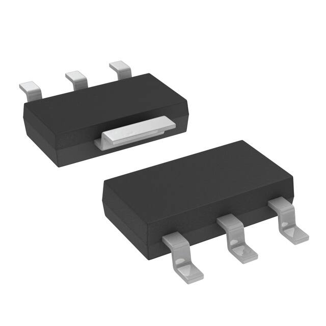
SOT223
AUIPS2051L
SO-8
AUIPS2052G
Typical Connection
+Bat
Load
D
2
S
3
IN
Control
Input R
Input Signal
V Diag
www.irf.com
1
1
�AUIPS2051L/AUIPS2052G
Qualification Information†
Qualification Level
Automotive
††
(per AEC-Q100 )
Comments: This IC has passed an Automotive qualification. IR’s
Industrial and Consumer qualification level is granted by extension of
the higher Automotive level.
††
SOT-223
MSL2 , 260°C
(per IPC/JEDEC J-STD-020)
8L-SOICN
MSL2 , 260°C
(per IPC/JEDEC J-STD-020)
Moisture Sensitivity Level
††
Machine Model
ESD
Human Body Model
Charged Device Model
IC Latch-Up Test
RoHS Compliant
†
††
Class M3
(per AEC-Q-100-003)
Class H2
(per AEC-Q-100-002)
Class C5
(per AEC-Q-100-011)
ClassII, Level A
(per AEC-Q100-004)
Yes
Qualification standards can be found at International Rectifier’s web site http://www.irf.com/
Exceptions to AEC-Q100 requirements are noted in the qualification report.
www.irf.com
2
�AUIPS2051L/AUIPS2052G
Absolute Maximum Ratings
Absolute maximum ratings indicate sustained limits beyond which damage to the device may occur. All voltage parameters
are referenced to Ground lead. (Tambient=25°C unless otherwise specified).
Symbol
Parameter
Min.
Max.
Units
Vds
Vds cont.
Vin
Isd cont.
Maximum drain to source voltage
Maximum continuous drain to source voltage
Maximum input voltage
Max diode continuous current (limited by thermal dissipation) Rth=125°C/W
Maximum power dissipation (internally limited by thermal protection)
Rth=60C°/W AUIPS2051L 1” sqr. footprint
Rth=100°C/W AUIPS2052G std. footprint
Electrostatic discharge voltage (Human body) C=100pF, R=1500
Between drain and source
Other combinations
Electrostatic discharge voltage (Machine Model) C=200pF,R=0
Between drain and source
Other combinations
Max. storage & operating temperature junction temperature
-0.3
-0.3
60
35
6
1
V
V
V
A
2
1.25
4
3
-40
0.5
0.3
150
°C
Typ.
Max.
Units
100
60
100
130
Pd
ESD
Tj max.
W
kV
Thermal Characteristics
Symbol
Parameter
Rth1
Rth2
Thermal resistance junction to ambient SOT-223 std. footprint
Thermal resistance junction to ambient SOT-223 1” sqr. footprint
Thermal resistance junction to ambient SO-8 std. Footprint
Rth1
Rth1
1 die active
Thermal resistance junction to ambient SO-8 std. footprint
2 die active
°C/W
note : Tj=Power dissipated in one channel x Rth
Recommended Operating Conditions
These values are given for a quick design. For operation outside these conditions, please consult the application notes.
Symbol
Parameter
VIH
VIL
Ids
Rin
Max. t rise
High level input voltage
Low level input voltage
Continuous drain current, Tambient=85°C, Tj=125°C, Vin=5V,Rth=100°C/W
Recommended resistor in series with IN pin to generate a diagnostic
Max. input rising time
www.irf.com
Min.
Max.
Units
4
0
5.5
0.5
0.9
5
1
A
k
µs
0.5
3
�AUIPS2051L/AUIPS2052G
Static Electrical Characteristics
Tj=-40..150°C, Vcc=28V (unless otherwise specified)
Symbol
Parameter
Rds(on)
ON state resistance Tj=25°C
ON state resistance Tj=150°C(2)
Drain to source leakage current
Drain to source leakage current
Drain to source clamp voltage 1
Drain to source clamp voltage 2
IN to source pin clamp voltage
Input threshold voltage
ON state IN positive current
OFF state IN positive current
( after protection latched )
Idss1
Idss2
V clamp1
V clamp2
Vin clamp
Vth
Iin, on
Iin, off
Min.
Typ.
Max.
300
520
1
2
5.5
1.1
15
150
250
440
0.2
0.5
69
70
6.2
2
40
250
75
7.5
2.7
80
350
µA
Min.
Typ.
Max.
Units
0.1
0.1
1
0.1
1
0.3
1.8
0.5
5
3
2.5
3.5
2.5
Min.
Typ.
Max.
63
Units
m
µA
V
Test Conditions
Vin=5V, Ids=1A
Vcc=28V, Tj=25°C
Vcc=50V, Tj=25°C
Id=20mA See fig. 3 & 4
Id=150mA
Iin=1mA
Id=50mA
Vin=5V
Switching Electrical Characteristics
Vcc=28V, Resistive load=50, Rinput=50, Vin=5V, Tj=25°C
Symbol
Parameter
Tdon
Tr
Tdoff
Tf
Eon + Eoff
Turn-on delay time to 20%
Rise time 20% to 80%
Turn-off delay time to 80%
Fall time 80% to 20%
Turn on and off energy
µs
Test Conditions
See figure 2
µJ
Protection Characteristics
Tj=-40..150°C, Vcc=28V (unless otherwise specified)
Symbol
Parameter
Tsd
Over temperature threshold
Isd
Over current threshold
Vreset
IN protection reset threshold
Treset
Time to reset protection
(2) Guaranteed by design
www.irf.com
150(2)
1.2
1.1
15(2)
165
1.8
1.6
50
3
2
500
Units
°C
A
V
µs
Test Conditions
See figure 1
See figure 1
Vin=0V, Tj=25°C
4
�AUIPS2051L/AUIPS2052G
Lead Assignments
Functional Block Diagram
All values are typical
DRAIN
66V
1k
6V
S
R
75V
20k
Q
Q
Tj > 165°C
1k
75
150k
IN
I > Isd
SOURCE
www.irf.com
5
�AUIPS2051L/AUIPS2052G
All curves are typical values. Operating in the shaded area is not recommended.
Vin
Ids
tT reset
Ishutdown
Vin
Isd
20%
Tr-in
80%
Tj
Ids
Tsd
165°C
20%
Tshutdown
Td on
Td off
Tr
Vdiag
Tf
Vds
normal
fault
Figure 1 – Timing diagram
Figure 2 – IN rise time & switching definitions
T clamp
Vin
L
Rem : During active clamp,
Vload is negative
V load
R
Ids
D
Vds clamp
IN
5V
Vds
+
14V
-
Vin
0V
Vcc
Vds
S
Ids
See Application Notes to evaluate power dissipation
Figure 3 – Active clamp waveforms
www.irf.com
Figure 4 – Active clamp test circuit
6
�AUIPS2051L/AUIPS2052G
200%
150%
100%
50%
0%
0
1
2
3
4
5
6
Rds(on), Drain-to-Source On Resistance
(Normalized)
Rds(on), Drain-to-Source On Resistance
(normalized)
200%
150%
100%
50%
-50
Vin, input voltage (V)
0
50
100
150
Tj, junction temperature (°C)
Figure 5 – Normalized Rdson (%) Vs Input voltage (V)
Figure 6 - Normalized Rds(on) (%) Vs Tj (°C)
2
140%
Isd, normalized I shutdown (%)
120%
Ids, output current
1.5
1
0.5
I limit
I shutdown
0
100%
80%
60%
40%
20%
0%
0
1
2
3
4
5
6
Vin, input voltage (V)
Figure 7 – Current limitation and current shutdown
Vs Input voltage (V)
www.irf.com
-50
0
50
100
150
Tj, junction temperature (°C)
Figure 8 – Normalized I shutdown (%) Vs junction
temperature (°C)
7
�2
Ids, cont. Output current (A)
SOT223
Rth=100°C/W
1
0
-50
0
50
100
150
Tamb, Ambient temperature (°C)
Idss1, drain to source leakage current 28V (µA)
AUIPS2051L/AUIPS2052G
Figure 9 – Max. continuous output current (A) Vs
Ambient temperature (°C)
1.4
1.2
1
0.8
0.6
0.4
0.2
0
-50
0
50
100
150
Temperature (°C)
Figure 10 – Idss1 (µA) Vs temperature (°C)
1
0.1
0.1
1
10
100
1000
Inductive load (mH)
Figure 11 – Max. ouput current (A)
Vs Inductive load (mH)
Zth, transient thermal impedance (°C/W)
Ids, output current (A)
10
100
10
1
0.1
0.01
1E-5 1E-4
1E-3 1E-2
1E-1 1E+0 1E+1 1E+2 1E+3
Time (s)
Figure 12 – Transient thermal impedance (°C/W)
Vs time (s)
This is for single pulse when Tj=165°C and for repetitive
pulses when Tj
很抱歉,暂时无法提供与“AUIPS2051L”相匹配的价格&库存,您可以联系我们找货
免费人工找货