Automotive grade
AUIR3320S
LOW EMI CURRENT SENSE HIGH SIDE SWITCH
Features
Product Summary
Load current feedback
Programmable over current shutdown
Active clamp
ESD protection
Input referenced to Vcc
Over temperature shutdown
Switching time optimized for low EMI
Reverse battery protection
Lead-Free, Halogen-Free, RoHS compliant
Rds(on)
4 m max.
Vcc op.
6 to 26V
Current Ratio
6000
Prog. Ishutdown 10 to 55A
Vclamp
40V
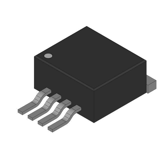
Packages
Description
The AUIR3320(S) is a fully protected 4 terminals high side
switch. The input signal is referenced to Vcc. When the
input voltage Vcc - Vin is higher than the specified
threshold, the output power Mosfet is turned on. When the
Vcc - Vin is lower than the specified Vil threshold, the
output Mosfet is turned off. A current proportional to the
power Mosfet current is sourced to the Ifb pin. Over
current shutdown occurs when Vifb-Vin > 4.7V. The
current shutdown threshold is adjusted by selecting the
proper RIfb. Either over current and over temperature
latches off the switch. The device is reset by pulling the
input pin high. Other integrated protections (ESD, reverse
battery, active clamp) make the switch very rugged in
automotive environment.
D²Pak
Pin 4 and 5 fused
AUIR3320S
Ordering Information
Base Part Number
Standard Pack
Package Type
Complete Part Number
Form
AUIR3320S
1
D2-Pak-5-Leads
Tape and reel left
Quantity
800
AUIR3320STRL
2017-07-11
�AUIR3320S
Typical Connection
Vcc
In
Current feedback
Input
Battery
Ifb
10k
OR
AUIR3320S
*
Out
Rifb
Load
On
Off
Logic
Ground
Power
Ground
*The diode between the collector and the emitor is necessary for the reverse battery protection
2
2017-7-11
�AUIR3320S
Absolute Maximum Ratings
Absolute maximum ratings indicate sustained limits beyond which damage to the device may occur. All voltage parameters
are referenced to Vcc lead. (Tj=-40°..150°C, Vcc=6.26V Tambient=25°C unless otherwise specified).
Symbol
Parameter
Vcc-Vin
Vcc-Vin cont.
Vcc-Vfb
Vcc-Vout
Ids cont.
Ids pulsed
Pd
Maximum Vcc voltage
Maximum continuous Vcc voltage
Maximum Ifb voltage
Maximum output voltage
Maximum body diode continuous current Rth=60°C/W (1) Tambient=25°C
Maximum body diode pulsed current (1)
Maximum power dissipation Rth=60°C/W Tambient=25°C
Maximum operating junction temperature
Tj max.
Maximum storage temperature
Min Rfb
Minimum on the resistor on Ifb pin
Ifb max.
Max. Ifb current
(1) Limited by junction temperature. Pulsed is also limited by wiring
Min.
Max.
-16
-16
-16
-0.3
37
26
33
37
2.8
100
2
150
150
-40
-55
0.3
-50
Units
V
A
W
°C
50
k
mA
Typ.
Max.
Units
60
40
0.7
°C/W
Thermal Characteristics
Symbol
Parameter
Rth1
Rth2
Rth3
Thermal resistance junction to ambient D²-Pak Std footprint
Thermal resistance junction to ambient D²-Pak 1” sqrt. footprint
Thermal resistance junction to case D²-Pak
Recommended Operating Conditions
These values are given for a quick design. For operation outside these conditions, please consult the application notes.
Symbol
Parameter
Continuous output current
Iout
Tambient=85°C, Rth=5°C/W, Tj=150°C
Tambient=85°C, Rth=40°C/W, Tj=150°C
Rifb
Recommended Ifb resistor (2)(3)
Pulse min.
Minimum turn-on pulse width
Fmax.
Maximum operating frequency
(2) If Rifb is too low, the device can be damaged.
(3) If Rifb is too high, the device may not switch on.
3
Min.
Max.
Units
45
16
3.5
A
0.3
1
200
k
ms
Hz
2017-7-11
�AUIR3320S
Protection Characteristics
Tj=-40°..150°C, Vcc=6..26V, Rifb=500 to 3.5k. Typical value are given for Vcc=14V and Tj=25°C
Symbol
Parameter
Vifb-Vin@Isd
Tsd
OV
Isdf
Isd_560
Treset
Min. pulse
WAIT
Over-current shutdown threshold
Over temperature threshold
Over voltage protection (not latched)
Fixed over current shutdown
Programmable over current shutdown
Time to reset protection
Min. pulse width (no WAIT state)
WAIT function timer
Reverse battery On state resistance,
Tj=25°C
Tj=125°C
Rds(on) rev.
Min.
Typ.
Max.
Units
3.8
5.9
33
105
71
500
2000
2
V
°C
V
0.4
4.7
165
29
75
50
50
900
1
4
6
6
9
26
55
34
A
µs
ms
m
Test Conditions
See fig. 5
Vifb 75A
Tj > 165°C
IN
5
+
Min. Pulse
reverse
battery
protection
IFB OUT
2017-7-11
�AUIR3320S
Lead Assignments
3- Vcc
1- In
2- Ifb
3- Vcc (tab)
4- Out
5- Out
12
45
D²Pak
90%
90%
Vcc-Vin
Vih
Vil
Vhyst
Icc
Vcc
Vcc-Vout
Vclamp1
Vclamp2
Vcc-Vin
10%
tr-in Tr-in
90%
Vcc-5V
IN
90%
Vcc-5V
IR3320
Iin
Ifb
10%
10%
Td on
Vout
Out
Td off
Tr1
10%
Tf
td on
Ifb
Iout
Isd
Figure 1 – Voltages and current definitions
6
Tr2
td off
tr1
tf
tr2
Figure 2 – Switching time definitions
2017-7-11
�AUIR3320S
t clamp
Vcc-Vin
Vin
Iout
t min. pulse
Vcc
t min. pulse
Wait
Iout
Vout
Vcc - V clamp
See Application Notes to evaluate power dissipation
Figure 3 – Active clamp waveforms
Figure 4 – Min. pulse and Wait function
Vcc-Vin
t < t reset
t > t reset
t < t reset
Wait
t > t reset
Wait
Over-current shutdown
Iout
Over-temperature shutdown
Tj
Figure 5 – Protection Timing Diagrams
7
2017-7-11
�AUIR3320S
All curves are typical characteristics. Tj=25°C, Rifb=500ohm, Vcc=14V (unless otherwise specified).
6
Icc, supply current (mA)
8
6
4
2
0
0
10
20
30
40
50
Icc off, supply leakeage current (µA)
10
5
4
3
2
1
0
-50
0
Vcc-Vin, supply voltage (V)
150
Figure 7 – Icc off (µA) Vs Tj (°C)
6
180%
Rds(on), Drain-to-Source On Resistance
(Normalized)
100
Tj, junction temperature (°C)
Figure 6 – Icc (mA) Vs Vcc-Vin (V)
160%
Vih, Vil and Vifb-Vin@Isd (V)
5
140%
120%
100%
80%
60%
40%
20%
4
Vifb-Vin@Isd
VIH
3
VIL
2
1
0
-50
0%
-50 -25
0
25
50
-25
0
25
50
75
100
125
150
75 100 125 150
Tj, junction temperature (°C)
Figure 8 - Normalized Rds(on) (%) Vs Tj (°C)
8
50
Tj, junction temperature (°C)
Figure 9 – Vih, Vil and Vifb-Vin@Isd (V) Vs Tj (°C)
2017-7-11
�AUIR3320S
100
12
With calibration
Isd, over current shutdown (A)
10
Spec. Max.
Error (+/-A)
8
6
4
2
0
0
20
10
40
100
I load, load current (A)
1000
10000
Rifb, feedback resistor ()
Figure 10 – Error (+/- A) Vs I load (A)
Figure 11 – Ids (A) Vs Rifb ()
40
100
60°C/W
35°C/W
Max. output current (A)
Max. output current (A)
30
20
10
10
0
-50
0
50
100
150
Tamb., ambient temperature (°C)
Figure 12 – Max. Iout (A) Vs Tamb. (°C)
9
10
100
1000
Inductance (µH)
Figure 13 – Max. Iout (A) Vs inductance (µH)
2017-7-11
�AUIR3320S
Zth, transient thermal impedance (°C/W)
100
50°C/W free air
5°C/W
10
1
0.1
1.E-4
1.E-3
1.E-2
1.E-1
1.E+0 1.E+1 1.E+2
Time (s)
Figure 14 – Transient thermal impedance (°C/W)
Vs time (s)
10
2017-7-11
�AUIR3320S
Case Outline - D2PAK - 5 Leads
11
2017-7-11
�AUIR3320S
Tape & Reel - D2PAK – 5 leads
12
2017-7-11
�AUIR3320S
Part Marking Information
Qualification Information†
Qualification Level
Moisture Sensitivity Level
Machine Model
ESD
Human Body Model
Charged Device Model
IC Latch-Up Test
RoHS Compliant
13
Automotive
(per AEC-Q100)
Comments: This family of ICs has passed an Automotive qualification. IR’s
Industrial and Consumer qualification level is granted by extension of the
higher Automotive level.
D2PAK-5L
MSL1, 260°C
(per IPC/JEDEC J-STD-020)
Class M3 (400V)
(per AEC-Q100-003)
Class H2 (4,000 V)
(per AEC-Q100-002)
Class C4 (1000 V)
(per AEC-Q100-011)
Class II, Level A
(per AEC-Q100-004)
Yes
2017-7-11
�AUIR3320S
Published by
Infineon Technologies AG
81726 München, Germany
© Infineon Technologies AG 2015
All Rights Reserved.
IMPORTANT NOTICE
The information given in this document shall in no event be regarded as a guarantee of conditions
or characteristics (“Beschaffenheitsgarantie”). With respect to any examples, hints or any typical
values stated herein and/or any information regarding the application of the product, Infineon
Technologies hereby disclaims any and all warranties and liabilities of any kind, including without
limitation warranties of non-infringement of intellectual property rights of any third party.
In addition, any information given in this document is subject to customer’s compliance with its
obligations stated in this document and any applicable legal requirements, norms and standards
concerning customer’s products and any use of the product of Infineon Technologies in
customer’s applications.
The data contained in this document is exclusively intended for technically trained staff. It is the
responsibility of customer’s technical departments to evaluate the suitability of the product for the
intended application and the completeness of the product information given in this document with
respect to such application.
For further information on the product, technology, delivery terms and conditions and prices
please contact your nearest Infineon Technologies office (www.infineon.com).
WARNINGS
Due to technical requirements products may contain dangerous substances. For information on
the types in question please contact your nearest Infineon Technologies office.
Except as otherwise explicitly approved by Infineon Technologies in a written document signed by
authorized representatives of Infineon Technologies, Infineon Technologies’ products may not be
used in any applications where a failure of the product or any consequences of the use thereof
can reasonably be expected to result in personal injury
14
2017-7-11
�AUIR3320S
Revision History
Revision
Date
A7
A8
June, 4 2012
August, 13rd 2012
Notes/Changes
A9
Rev1.0
August, 30 2012
th
July, 11 2017
th
15
th
Initial release
-Update switching limits
-Update Iratio max limit
Update Tj max.
- Page ‘Case Outline - D2PAK - 5 Leads’
updated
- Page ‘Ordering information’ updated
- Page 14 ‘Notice’ updated
2017-7-11
�