Automotive Grade
AUIR3330S
PROTECTED HIGH FREQUENCY HIGH SIDE SWITCH
Features
Applications
Up to 30Khz PWM switching capability
Charge pump for DC operation
Active di/dt control to reduce EMI
Load current feedback
Short-circuit protection
Programmable over current shutdown
Over temperature shutdown
Diagnostic feedback
Under voltage shutdown
Gnd, IN and bootstrap pin loss protection
E.S.D protection
Low power mode
Lead-free, RoHS compliant
Fan engine cooling
Air conditioning blower
Pumps (oil, fuel, water…)
Compressor
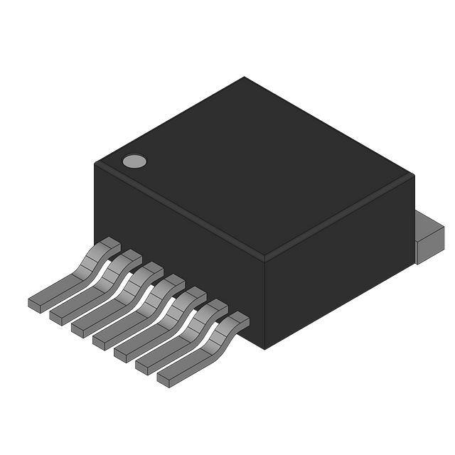
Package
D2Pak - 7 leads
Description
The AUIR3330s is a 7 terminals high side switch for variable speed DC motor. It features simplify the design of
the DC motor drive with a microcontroller. The Mosfet switches the power load proportionally to the input signal
duty cycle at the same frequency and provides a current feedback on the Ifbk pin. The over-current shutdown is
programmable from 5A to 50A. Over-current, over-temperature latch OFF the power switch and provide a digital
diagnostic status on the input pin. In sleep mode, the device consumes typically less then 1uA.
Further integrated protections such as ESD and GND disconnect protection guarantee safe operation in harsh
conditions of the automotive environment.
Typical connection with reverse battery protection
1
www.irf.com
© 2012 International Rectifier
May 29, 2014
�AUIR3330S
Qualification Information†
Automotive
(per AEC-Q100)
Comments: This family of ICs has passed an Automotive
qualification. IR’s Industrial and Consumer qualification level is
granted by extension of the higher Automotive level.
Qualification Level
Moisture Sensitivity Level
Machine Model
ESD
Human Body Model
Charged Device Model
IC Latch-Up Test
RoHS Compliant
MSL1 260°C
(per IPC/JEDEC J-STD-020)
Class M3 (+/-350V)
(per AEC-Q100-003)
Class H4 (+/-4000V)
(per AEC-Q100-002)
Class C4 (Pass +/-1000V)
(per AEC-Q100-011)
Class II Level A
(per AEC-Q100-004)
Yes
† Qualification standards can be found at International Rectifier’s web site http://www.irf.com/
2
www.irf.com
© 2012 International Rectifier
May 29, 2014
�AUIR3330S
Absolute Maximum Ratings
Absolute maximum ratings indicate sustained limits beyond which damage to the device may occur.
(Tj= -40°C..150°C, Vcc=6..18V unless otherwise specified).
Symbol
Parameter
Min.
Max.
Vout
Maximum drain to source voltage
GND-5V
Vcc+0.3
Vin
Maximum input voltage
-0.3
5.5
Vcc max.
Maximum Vcc voltage
36
Vcc cont
Maximum continuous Vcc voltage
28
Iin max.
Maximum input current
-0.3
10
Ifb max
Maximum Ifb current
-50
10
Maximum power dissipation
Rth=60°C/W
Pd
2.5
Tambient=25°C, Tj=150°C Rth=40°C/W D²Pack 6cm² footprint
Tj max.
Max. storage & operating temperature junction temperature
-40
150
Units
V
V
V
V
mA
mA
W
°C
Thermal Characteristics
Symbol
Rth1
Rth2
Rth3
Parameter
Thermal resistance junction to ambient D²Pak Std footprint
Thermal resistance junction to ambient D²pak 6cm² footprint
Thermal resistance junction to case D²pak
Typ.
60
40
0.65
Max.
Units
Min.
6
100
100
2.2
1
10
1
0.6
Max.
18
45
220
5
50
2.2
5
Units
V
A
nF
nF
µF
k
k
nF
k
10
25
k
30
kHz
°C/W
Recommended Operating Conditions
These values are given for a quick design.
Symbol
Parameter
Vcc op.
Operating voltage range
Iout
DC output current Tj=145°C, Tamb=85°C, Rth=5°C/W
Cboot
Bootstrap capacitor
Cd1
Decoupling ceramic capacitor
Cd2
Decoupling ceramic capacitor
R In
Recommended resistor in series with In pin
Rp diag
Recommended resistor in series with In pin to read the diagnostic
CIfb
Recommended Ifb filter capacitor
RIfb
Recommended resistor to program over current shutdown
Recommended resistor in series with RIfb pin to read the current
Rp Ifb
feedback
Maximum recommended input frequency, duty cycle=10% to 90%
F max.
3
www.irf.com
© 2012 International Rectifier
May 29, 2014
�AUIR3330S
Static Electrical Characteristics
-40°C < Tj < 150°C, 6V < Vcc < 18V, (unless otherwise specified)
Symbol
Parameter
Min.
Typ.
ON state resistance Tj=25°C
3
Rds on
1
ON state resistance Tj=150°C
5.5
ON state resistance low voltage
Rds on Lv
3
Tj=25°C
Forward voltage of the Mosfet body
Vf Mos
0.6
diode
Breakdown voltage between Vcc
Vbrk out
39
40
and Vout (MOSFET body diode)
Supply current in sleep mode (IC +
I Vcc Slp
1
MOSFET leakage)
Bootstrap regulator biasing current
I bias Boot
5.5
(flows through the output)
Vcc current when the device is
I Vcc Wke
14
woken up (IC + Ibias Boot)
Input threshold voltage to wake up
V In Wke
0.35
0.75
the device
V In Off
In voltage threshold to turn off
1.9
2.2
V In On
In voltage threshold to turn on
2.8
V In Hyst
Input threshold hysteresis
0.4
C In
Input pin capacitor
10
I In on
On state input current
10
20
Max.
3.5
6.2
Units
3.5
m
1.1
V
V
2
µA
Vin=0V Vcc = 14V
Tj = 25°C
14
mA
Vout = 0V
20
mA
I_boot = 0A Vout = 0V
1.3
V
3.2
0.7
30
V
V
V
pF
µA
m
I Bt Chrge
Bootstrap current charge
0.4
1.5
A
V Bt Chrge
Bootstrap voltage
4.9
5.5
6.3
V
Test Conditions
Iout=30A
Iout=30A
Iout=15A Vcc=6V
Iout = -50A
Vin = 5V
Vout = 0V
Cboot =500nF
Cboot =500nF
Guaranteed by design.
4
www.irf.com
© 2012 International Rectifier
May 29, 2014
�AUIR3330S
Switching Electrical Characteristics
-40°C < Tj < 150°C, 6V < Vcc < 18V, Rin = 5k (unless otherwise specified)
Symbol
Parameter
Min.
Typ.
Max.
Units
Td Vout on
Turn-on output voltage delay time
0.7
1
1.4
µs
Tr Vout
Ouput voltage rise time
500
800
1300
ns
Tr Iout
Ouput current rise time
0.7
1.2
1.85
µs
dv/dt on
Turn on dv/dt
10
20
28
V/µs
di/dt on
Turn on di/dt
21
40
51
A/µs
Td Vout off
Turn-off delay time
0.9
1.2
1.7
µs
Tf Vout
Output voltage fall time
250
430
650
ns
Tf Iout
Output current fall time
0.55
1
1.45
µs
dv/dt off
Turn off dv/dt
28
50
67
V/µs
di/dt off
Turn off di/dt
30
40
51
A/µs
8.5
10
11.5
µs
38.5
39.5
40.5
µs
2
µs
T Trfct Ld
T Trfct Hd
T Off Min
5
Input output transfer function for
low duty cycle
Input output transfer function for
high duty cycle
Minimum off time to recharge the
bootstrap capacitor
www.irf.com
© 2012 International Rectifier
Conditions
between 50% of IN and
30% of Vout, Iout = 14A
Between 15% and 85%;
Vcc = 14v, Iout=14A
Between 5A and 40A;
Vcc = 14v, Iout=45A
Between 25% and 70%;
Vcc = 14v
Between Iout 15A and
35A; Vcc = 14v
between 50% of IN and
90% of Vout, Iout = 14A
Between 90% and 10%;
Vcc = 14v, Iout=14A
Between 40A and 5A;
Vcc = 14v, Iout=45A
Between 30% and 70%;
Vcc = 14v
Between Iout 35A and
15A; Vcc = 14v
Iout = 1A;
In pulse time =10µS
Iout = 1A;
In pulse time =40µS
Cboot = 100nF
May 29, 2014
�AUIR3330S
Protection Characteristics
-40°C < Tj < 150°C, 6V < Vcc < 18V (unless otherwise specified).
Symbol
Parameter
Min.
Typ.
Vth Ifb
IFB over current threshold voltage
3.65
4
Maximum internal over current
Isd fix
55
70
shutdown
Isd prog 2
Programmable current shutdown
11
17
Isd prog 1
Programmable current shutdown
30
40
2
Tsd
Over temperature threshold
150
165
Vds threshold to activate the over
Vth Vds OVP
0.75
power protection
Vds delay to turn off after OVP
Td Vds OVP
6
10
detection
UV On
5.3
Under voltage threshold to turn on
UV Off
4.3
Under voltage threshold to turn off
UV Hyst
Under voltage hysteresis
0.5
T slp
Sleep mode time and fault reset
20
30
T rst
Time to reset the latched fault
50
T wke min
Minimum pulse width to wake up
2
Tpwr_on_rst
Power on reset time
5
8
Over temperature diagnostic
F Dg OT
260
frequency
F Dg OC
Over current diagnostic frequency
35
70
V Dg Dft
DG voltage when fault
Max.
4.35
Units
V
Conditions
90
A
24
50
175
A
A
°C
Rifb = 1.5k
Rifb = 640
V
Tj=25°C
15
µs
6.3
5.3
1.25
50
15
V
V
V
ms
µs
µs
µs
Hz
95
400
Hz
mV
Tj=25°C
Vin = 5V Rin = 5k
Current Sense Characteristics
-40°C < Tj < 150°C, 6V < Vcc < 18V (unless otherwise specified), Rifbk=1k
Symbol
Parameter
Min.
Typ.
Max.
I offset
Load current diagnostic offset
-2.7
0.62
4
Ratio
(I load + I offset) / Ifb
5400
6400
7200
Ratio Tc
Iload/Ifbk variation over temperature
-3.5
1.5
2
Guaranteed by design.
6
www.irf.com
© 2012 International Rectifier
Units
A
%
Conditions
Range 5A to 40A
Range 5A to 40A
Tj=-40°C to 150°C
May 29, 2014
�AUIR3330S
Leads Assignment
PART NUMBER
1 : Ifb
2 : In
3 : Gnd
4 : Vcc (Tab)
5 : Boot
6 : Out
7 : Out
7
www.irf.com
© 2012 International Rectifier
AUIR3330S
D2Pak 7 leads
May 29, 2014
�AUIR3330S
Functional Block Diagram
All values are typical
Internal diode schematic
All values are typical
Boot
8
www.irf.com
© 2012 International Rectifier
May 29, 2014
�AUIR3330S
Design: basic schematic with microprocessor
The basic circuit is giving all the functionality to drive a 50A DC motor. RIfb set both the current shutdown and the
current feedback reading scale. The In signal provides the Pwm frequency and duty cycle order to the
AUIR3330S. D1 is the free wheeling diode during PWM operation. As the equivalent circuit between Vbat and –
Mot is 2 diode in series (the body diode of the AUIR3330S and D1), the system requires T1, D2, R1 and R2 to
sustain the reverse battery. (Cf: Typical connection with reverse battery protection).
DC to 30 kHz operation
The AUIR3330S is able to operate in DC and high speed switching operation. To be able to switch at 30 kHz, a
bootstrap capacitor is used externally. The device integrates the power supply of the bootstrap capacitor. In DC
operation, when the capacitor is discharged, the charge pump maintains the device ON.
Active di/dt control to reduce EMI and switching losses
Phase 7
Phase 6
Phase 5
Phase 4
Phase 3
On
Phase 1
Phase 2
The AUIR3330S includes a special gate drive, managing the Mosfet di/dt controlled internally, by managing the
gate voltage dynamically. This di/dt trade-off is set internally to an optimum value, between power dissipation
versus noise. This feature brings to the designer less EMI versus switching losses. The system has three phases
during the turn on sequence and three phases during the turn off sequence. First the driver injects a high current
in the gate until the gate voltage reaches the Vth. Then it injects a low current to control the di/dt value until the
gate voltage reaches the miller plate. And after it injects a high current to fully turn on quickly the MOSFET to
reduce the dv time (reducing the switching losses). The turn off sequence is the same than the turn on but in the
opposite direction: First reduce the dv time after control the di/dt and then discharge totally the gate.
Igate
Vgs
Vth
Ids
VDS
9
www.irf.com
© 2012 International Rectifier
Switching
losses losses
Switching
May 29, 2014
�AUIR3330S
Sense Load current feedback and programmable current shutdown
The Ifb pin allows an analog measurement of the load current and with an external resistor allows to program the
over current shutdown level from 10A to 50A. The voltage threshold level of the Ifb pin is internally set to 4v (See
the formulas below). It is also possible to dynamically adjust the current shutdown protection versus time by
adding some external components. This protection is latched and turns off the output MOSFET without di/dt
sequence to reduce the device and the application stress. The operating mode is recovered after resetting by the
sleep mode.
Rifb
Vifb _ gnd min
Ratio min
Imax _ appli Ioffset min
Ishd max MAX Ishd max@ 40C; Ishd max@ 25; Ishtd max@ 150C
Vifb min@ T C
Iload Ioffset max@ T C
Rifb
Ratio max@ T C
Vifb max@ T C
Iload Ioffset min@ T C
Rifb
Ratio min@ T C
Vifb _ gnd max
Ishd max@ T C
Ratio max@ T C Ioffset max@ T C
Rifb (calculated )
Where:
Imax appli is the maximum application current
Ishtd max is the maximum output shutdown current
Internal over current shutdown
The maximum current shutdown threshold value is internally fixed to 65A typ. This protection is latched and turns
off the output MOSFET without di/dt sequence to reduce the device and the application stress. The operating
mode is recovered after resetting by the sleep mode.
Under voltage lock-out
The AUIR3330S remains operational from UV off threshold. Under this continuous voltage, the device will be
locked until the voltage recovers the operating range, according to an internal hysteresis fixed to 0,5V min. The
maximum rating voltage is given by the Trench VDMOS technology where the avalanche voltage is up to 43V
typically.
Sleep mode and reset fault:
The sleep mode is enabled if the IN pin stay low (Vin < V In Slp) more than T Slp time. The consumption in sleep
mode is Icc off. The AUIR3330S wakes up at first rise edge on the IN pin (Vin > V In Slp). This mode allows
resetting all the latched faults after Trst time (Cf. Error! Reference source not found.). This filter time allows
memorizing and maintaining the fault latched even if the power supply is removed (ISO pulses latch protection).
10
www.irf.com
© 2012 International Rectifier
May 29, 2014
�AUIR3330S
Over-power protection
The AUIR3330S have an internal over-power protection. This feature allows protecting the silicon device and the
application against several critical issues:
The bootstrap capacitor missing.
Abnormal leakage on the bootstrap capacitor.
Abnormal leakage on the power MOSFET gate.
Very low impedance output short circuit.
ED_pch signal
Actif if Vgs > Vth
Igen1
• The time constant Ign1 + C represent the thermal
silicon time constant
R1
+
-
Vds_075 signal
Actif if Vds < 0.75 V
Sw1
C
Igen2
OVP_Flt signal
Go to the latch block
• The time constant Ign2 + C represent the thermal
package time constant (T(ign2 + C) < T Slp)
• Igen1 is on if the gate voltage (of the
output MOSFET) is higher than its Vth
R2
• Ign2 is always switching on.
• Sw1 is close if the Vbat – out voltage (Vds)
is lower than 0.75V
Time to charge the capacitor and latch a fault (Igen1 + C) = 9µs
Time to discharge the capacitor (Igen2 + C) = 11ms
When the Output MOSFET gate voltage reaches its output MOSFET Vth value, the current generator Igen1 start
to charge the capacitor C. Then three scenarios are possible:
1. The device turn on properly (Vds < 0.75v) and the capacitor C is discharged by the switch sw1. The device is
In input
ready for the next pulse. It is the normal
case.
Vgs voltage
Normal value
Vbat – Voutput voltage
(Vds)
2. The device can not turn on properly (Vds
stay > 0.75v no capacitor reset) and the on
time duration (duty cycle) is enough long to
charge completely the capacitor C. The
comparator detects the fault, stop the
device and latch it. This fault could be reset
by a sleep mode
Ed_pch signal
C capacitor
voltage
OVP_Flt
signal
11
www.irf.com
© 2012 International Rectifier
May 29, 2014
�AUIR3330S
In input
3. The device can not turn on properly (Vds stay >
0.75v no capacitor reset) but the ON time duration
(duty cycle) is not enough long to charge
completely the capacitor C. So the fault is not
detected by the comparator and it is not latched.
But the picture of energy value dissipated by the
MOSFET during the almost turn on value is stored
in the capacitor C. And at the next pulse the
current generator Igen1 resume to charge the
capacitor until it reach the comparator value and
latch the fault (this sequence could be on several
pulse). It could be reset by a sleep mode.
Vgs voltage
Normal value
Vbat – Voutput voltage
(Vds)
Ed_pch signal
C capacitor
voltage
OVP_Flt
signal
Wake up sequence:
The AUIR3330S has an internal power on reset. After waking it up by the IN signal, the device waits for
Tpwron_rst before activating the output power mosfet. This time is required to charge properly the bootstrap
capacitor and to stabilize the internal power supply (Cf. Error! Reference source not found.).
12
www.irf.com
© 2012 International Rectifier
May 29, 2014
�AUIR3330S
In pin and digital diagnostic
The IN has two functions. In normal working condition, the output follows the IN pin digital level. In latched fault
condition (over current and over temperature shutdown), the IN pin provides a digital feedback to the µ-processor.
This digital diagnostic gives a different frequency signal according to the fault type.
13
www.irf.com
© 2012 International Rectifier
May 29, 2014
�AUIR3330S
Bootstrap current measurement:
Switching time definition:
As the opposite schematic shows, the dv/dt on & off and
the Td Vout on & off switching time are measured at zero
current value and with a simulated continuous conduction
condition to avoid the di/dt impact (see also the
chronogram above).
Due the inductive load, the drain current level impacts
directly the delay to switch on the output voltage. So the
output voltage duty cycle value changes with the current
level. The output current duty cycle is higher than the
output voltage duty cycle. The di/dt on limit value allows
calculating the complete delay (here named Tcdon and off)
to switch on the output voltage.
Tcdonmax Td _ Vout _ onmax
Tcdonmin Td _ Vout _ onmin
Tcdoff min Td _ Vout _ off min
Rin
4
8 AUIR3330S(L)
Vcc Tab
2
5
Vout
Boot
In
Cboot
1
100n
15v
If b
6
Out
7
Gnd Out2
Vcc
3
1 Ohm
14v
Figure 1: Switching time test circuit
Id
didt _ onmin
Id
didt _ onmax
Tonmin Tin _ on Tdconmax Tcdoff min
Tonmax Tin _ on Tdconmin Tcdoff max
Tcdoff max Td _ Vout _ off max
All switching time values (except the Td Vout on & off parameters) could change with the application schematic
(output snubber filter) and with the PCB layout. Due to the internal pad, the input pin of the device has a parasitic
capacitor Cin. This capacitor and the Rin (the recommended input resistor) create low pass filter and add an
additional delay in the Tdcon value.
14
www.irf.com
© 2012 International Rectifier
May 29, 2014
�AUIR3330S
The minimum off time is the time to charge the bootstrap capacitor (recover the value before turn on the
MOSFET) during the high duty cycle operation. In the high duty cycle value condition, due to the di/dt driver, the
internal gate continues to move whereas the output voltage doesn’t go down under 6v (from vbat). So the device
still need energy from the bootstrap capacitor but it can not charge it. When the bootstrap capacitor is discharged
the circuit goes in linear mode and it is stopped by the over power protection. To avoid this situation, the microprocessor must turn fully on the device after the minimum off time is reached as it is describe in the Error!
Reference source not found.. The minimum off time is the minimum time to charge properly the bootstrap
capacitor.
15
www.irf.com
© 2012 International Rectifier
May 29, 2014
�AUIR3330S
Notes:
Decoupling capacitors:
During the turn on and off phase, a high current
(about a hundred mA) flows through the Vcc, the
gnd and the boot. So the bootstrap capacitor and the
decoupling must be as closer as possible. And it is
forbidden to implement a resistor in series with the
Gnd
pin.
Bootstrap capacitor charge:
The power on reset is necessary to charge the
bootstrap capacitor before turns on the power
mosfet. The bootstrap capacitor gets its charge
through the load. So the time to charge it depends of
the load.
But the power on reset doesn’t monitor the bootstrap
capacitor voltage. Its time is set internally to allow
starting the most of load without implement a special
sequence:
Power on reset
time
Vin
Vcboot
Vboot
charged
Vg
If the inductance of the load is lower than 500µH, the power on
reset is enough long to charge the bootstrap capacitor before turns on
the power mosfet.
Time to charge the
bootstrap capacitor
16
www.irf.com
© 2012 International Rectifier
May 29, 2014
�AUIR3330S
Power on reset
time
Vin
T wakemin
If the inductance of the load is higher than 500µH, the power on reset is not
enough long to charge completely the bootstrap capacitor before turns on the power
mosfet. So the micro-processor need to implement a special sequence to start the
device without activates the output power mosfet. The µp send one short pulse
(Twake min < short pulse < Tpwr_on_rst) then wait for the bootstrap capacitor is
totally charged and after provide the appropriate duty cycle.
Vboot
charged
Vg
Time to charge the
bootstrap capacitor
The bootstrap charge depends of the battery voltage, the bootstrap capacitor value and the inductance load
value.
Output high dv/dt immunity system:
The IR3330S has a high dv/dt immunity system. This
function creates a negative gate biasing if the output
voltage exceed 1.7V. So this device can be
implemented in an H-bridge configuration.
17
www.irf.com
© 2012 International Rectifier
May 29, 2014
�AUIR3330S
Open load detection function:
The bootstrap regulator bias provides a current on device
output. If the impedance between the Output and ground is
too high, after the turn off of the output mosfet, the output
never reaches the ground. So it becomes possible to detect
easily an open load condition when the device switches. In
fully on condition the open load condition will detect by the
current feedback (easy thanks to a high current condition).
+Bat
Boot
CBoot
Vcc
C2
100nF
In
Vbat
Out
8mA
6V
6V
Ifbk
Ifb
D1
MBR
3045CT
- Mot
Gnd
In the schematic below the component R7, Q1, R8, D2
create the detection open load and provide a logic level
diagnostic (open diag line) even if the battery in low voltage
condition.
18
www.irf.com
© 2012 International Rectifier
+ Mot
Reverse
battery
protection
Gnd
May 29, 2014
�AUIR3330S
EMI consideration:
At vehicle level:
This is typical schematic of a high frequency power module in a vehicle (see: Error! Reference source not
found.) with the parasitic element create by the connection wire. Between the battery and the module, the voltage
is almost constant and the current switch at the application frequency. The power line creates a parasitic
inductance with the current variation that generates voltage spike on the battery line. The level of this spike is
directly linked to the conducted emissions level on the battery line. So control the current variation or the di/dt
value reduces the conducted EMI level on the battery line. In this case use the AUIR3330 (active di/dt control)
allows reducing significantly the conduced EMI level.
By analogy between the module and the load (see: Error! Reference source not found.), due to the high
inductance value of the motor, the current is almost constant and the voltage switches at the application
frequency. Due to the parasitic capacitor of the load each voltage variation create current spike on the load line.
The level of this spike is directly linked to the radiated emissions level on the load line. So control the voltage
variation or the dv/dt value reduces the radiated EMI level. In this case use the AUIR3340 (active dv/dt control)
allows reducing significantly the radiated EMI level.
19
www.irf.com
© 2012 International Rectifier
May 29, 2014
�AUIR3330S
At module level:
This typical schematic takes into account the
created by the PCB tracks. Its impedance is
Ztrace R jL .
parasitic elements
2F
Due to the jL element, the current
line must be smooth to avoid the over voltage
Ul L
variation in each
spikes.
Di
Dt
The impedance value of the parasitic element
negligible compare to the motor impedance.
an important influence on the EMI
Z3 and Z6 are
So they don’t have
perturbation level.
Figure 2: typical schematic of a power
module
The parasitic component evaluation for DC and low frequency conditions are:
l
R
S
d e
2l
L 0.2 106 l ln(
) 0.5 0.22(
)
l
d e
Where:
20
www.irf.com
: material resistivity Cu = 1.7x10⁻⁸m
l : track length in m
S : track section in m² (d x e)
d : track width in m
e : track thickness in m
© 2012 International Rectifier
e
May 29, 2014
�AUIR3330S
Example:
If the copper track characteristic between the MOSFET pin and the free wheeling diode (parasitic element Z2) is:
So
l = 2 cm
R = 0.9m
d = 1mm
L = 8nH
e = 35µm
If the MOSFET switches without any slope control, the di/dt can reach 100A/µs. The overvoltage spike created by
the current variation in the parasitic inductance is then
Ul = 8n * (100/1E-6) = 800mv
Now, if the MOSFET slope is controlled and limited to 40A/µs. Then, the overvoltage spike created by the current
variation in the parasitic inductance is:
Ul = 8n * (40/1E-6) = 320mV
Even if the PCB tracks are short, their parasitic impedances are not negligible in 20 kHz application. Limiting the
current variation in these parasitic impedances reduces the overvoltage spikes so the noise level. For further
information about the PCB impedance effect see the application note named “Using the AUIR3330/40: PCB
layout recommendation” on the IR web site (www.irf.com).
Measured impact of the di/dt control:
If the device detects an over current condition, it turns off the output MOSFET without di/dt sequence to reduce
application stress. So a simple test, consists to look at the waveform before (pulse1) and during the over current
protection shutdown (pulse 2) to see the di/dt impact with the same condition (even if the dv/dt stay constant).
Black (Ch1) = In_pwm 5V/div
Red (Ch2) = drain current 10A/div
Green (Ch3) = Vds (drain source voltage)
5V/div
Blue (Ch4) = Vbat (battery voltage) in AC
mode 1V/div
21
www.irf.com
© 2012 International Rectifier
Pulse1
Pulse2
May 29, 2014
�AUIR3330S
Pulse1) Oscilloscope screenshot in normal
condition:
The perturbation on the Vbat line during the turn on
is due to the discontinuity of the current in the diode
and intensified by the current loop implemented
between the input filter and the device to measure
the drain current (di/dt).
2) Oscilloscope screenshot during the over current
shutdown:
This screenshot is the next pulse after this one
shows previously. The perturbation on the Vbat line
during the turn on is due to the discontinuity of the
current in the diode and intensified by the current
loop implemented between the input filter and the
device to measure the drain current (di/dt).
Remove the di/dt sequence only on the turn off increase strongly the perturbation level (more than 20dB) on the
power line even if the output dv/dt value doesn’t change.
Note that in this example, the di/dt on sequence is still activated. By analogy with the turn off, we can easily
guessed that the over all noise level will be increase if we could only keep the dv/dt on and remove the di/dt on.
22
www.irf.com
© 2012 International Rectifier
May 29, 2014
�AUIR3330S
Parameters curves:
23
www.irf.com
© 2012 International Rectifier
May 29, 2014
�AUIR3330S
24
www.irf.com
© 2012 International Rectifier
May 29, 2014
�AUIR3330S
25
www.irf.com
© 2012 International Rectifier
May 29, 2014
�AUIR3330S
Figure 20: Transient thermal impedance and model vs. time
26
www.irf.com
© 2012 International Rectifier
May 29, 2014
�AUIR3330S
Case Outline 7L D2PAK
27
www.irf.com
© 2012 International Rectifier
May 29, 2014
�AUIR3330S
28
www.irf.com
© 2012 International Rectifier
May 29, 2014
�AUIR3330S
Part Marking Information
Ordering Information
Base Part Number
Standard Pack
Package Type
Complete Part Number
Form
AUIR3330S
29
D2-Pak-7Leads
www.irf.com
Quantity
Tube
50
Tape and reel left
800
Tape and reel right
800
© 2012 International Rectifier
AUIR3330S
AUIR3330STRL
AUIR3330STRR
May 29, 2014
�AUIR3330S
IMPORTANT NOTICE
Unless specifically designated for the automotive market, International Rectifier Corporation and its subsidiaries
(IR) reserve the right to make corrections, modifications, enhancements, improvements, and other changes to its
products and services at any time and to discontinue any product or services without notice. Part numbers
designated with the “AU” prefix follow automotive industry and / or customer specific requirements with regards to
product discontinuance and process change notification. All products are sold subject to IR’s terms and conditions
of sale supplied at the time of order acknowledgment.
IR warrants performance of its hardware products to the specifications applicable at the time of sale in
accordance with IR’s standard warranty. Testing and other quality control techniques are used to the extent IR
deems necessary to support this warranty. Except where mandated by government requirements, testing of all
parameters of each product is not necessarily performed.
IR assumes no liability for applications assistance or customer product design. Customers are responsible for
their products and applications using IR components. To minimize the risks with customer products and
applications, customers should provide adequate design and operating safeguards.
Reproduction of IR information in IR data books or data sheets is permissible only if reproduction is without
alteration and is accompanied by all associated warranties, conditions, limitations, and notices. Reproduction of
this information with alterations is an unfair and deceptive business practice. IR is not responsible or liable for
such altered documentation. Information of third parties may be subject to additional restrictions.
Resale of IR products or serviced with statements different from or beyond the parameters stated by IR for that
product or service voids all express and any implied warranties for the associated IR product or service and is an
unfair and deceptive business practice. IR is not responsible or liable for any such statements.
IR products are not designed, intended, or authorized for use as components in systems intended for surgical
implant into the body, or in other applications intended to support or sustain life, or in any other application in
which the failure of the IR product could create a situation where personal injury or death may occur. Should
Buyer purchase or use IR products for any such unintended or unauthorized application, Buyer shall indemnify
and hold International Rectifier and its officers, employees, subsidiaries, affiliates, and distributors harmless
against all claims, costs, damages, and expenses, and reasonable attorney fees arising out of, directly or
indirectly, any claim of personal injury or death associated with such unintended or unauthorized use, even if such
claim alleges that IR was negligent regarding the design or manufacture of the product.
Only products certified as military grade by the Defense Logistics Agency (DLA) of the US Department of Defense
are designed and manufactured to meet DLA military specifications required by certain military, aerospace or
other applications. Buyers acknowledge and agree that any use of IR products not certified by DLA as militarygrade, in applications requiring military grade products, is solely at the Buyer’s own risk and that they are solely
responsible for compliance with all legal and regulatory requirements in connection with such use.
IR products are neither designed nor intended for use in automotive applications or environments unless the
specific IR products are designated by IR as compliant with ISO/TS 16949 requirements and bear a part number
including the designation “AU”. Buyers acknowledge and agree that, if they use any non-designated products in
automotive applications, IR will not be responsible for any failure to meet such requirements.
For technical support, please contact IR’s Technical Assistance Center
http://www.irf.com/technical-info/
WORLD HEADQUARTERS:
101 N. Sepulveda Blvd., El Segundo, California 90245
Tel: (310) 252-7105
30
www.irf.com
© 2012 International Rectifier
May 29, 2014
�