AUTOMOTIVE GRADE
PD - 97732
AUIRFZ48N
HEXFET® Power MOSFET
Features
l
l
l
l
l
l
l
l
l
Advanced Planar Technology
Low On-Resistance
Dynamic dv/dt Rating
175°C Operating Temperature
Fast Switching
Fully Avalanche Rated
Repetitive Avalanche Allowed
up to Tjmax
Lead-Free, RoHS Compliant
Automotive Qualified*
D
G
S
V(BR)DSS
55V
RDS(on) typ.
max
ID
11m
14m
69A
D
Description
Specifically designed for Automotive applications, this
Stripe Planar design of HEXFET® Power MOSFETs utilizes the latest processing techniques to achieve low onresistance per silicon area. This benefit combined with
the fast switching speed and ruggedized device design
that HEXFET power MOSFETs are well known for, provides the designer with an extremely efficient and reliable device for use in Automotive and a wide variety of
other applications.
G
D
S
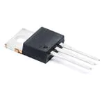
TO-220AB
AUIRFZ48N
G
Gate
D
Drain
S
Source
Absolute Maximum Ratings
Stresses beyond those listed under “Absolute Maximum Ratings” may cause permanent damage to the device. These are stress ratings
only; and functional operation of the device at these or any other condition beyond those indicated in the specifications is not implied.
Exposure to absolute-maximum-rated conditions for extended periods may affect device reliability. The thermal resistance and power
dissipation ratings are measured under board mounted and still air conditions. Ambient temperature (T A) is 25°C, unless otherwise
specified.
Parameter
Max.
Units
ID @ TC = 25°C
Continuous Drain Current, VGS @ 10V
69
ID @ TC = 100°C
Continuous Drain Current, VGS @ 10V
49
IDM
Pulsed Drain Current
270
PD @TC = 25°C
Power Dissipation
160
W
Linear Derating Factor
1.1
W/°C
Gate-to-Source Voltage
± 20
V
265
mJ
VGS
c
EAS
Single Pulse Avalanche Energy (Thermally Limited)
EAS (tested)
Single Pulse Avalanche Energy Tested Value
IAR
Avalanche Current
EAR
Repetitive Avalanche Energy
TJ
Operating Junction and
TSTG
Storage Temperature Range
�c
g
Soldering Temperature, for 10 seconds
Mounting Torque, 6-32 or M3 screw
h
d
290
See Fig.12a, 12b, 15, 16
i
mJ
°C
300 (1.6mm from case )
y
y
10 lbf in (1.1N m)
Typ.
Max.
–––
0.95
RJC
Junction-to-Case
RCS
Case-to-Sink, Flat, Greased Surface
0.50
–––
RJA
Junction-to-Ambient
–––
62
www.irf.com
A
-55 to + 175
Thermal Resistance
Parameter
A
Units
°C/W
1
10/3/11
�AUIRFZ48N
Static Electrical Characteristics @ TJ = 25°C (unless otherwise specified)
Parameter
V(BR)DSS
V(BR)DSS/TJ
RDS(on)
VGS(th)
gfs
IDSS
IGSS
Drain-to-Source Breakdown Voltage
Breakdown Voltage Temp. Coefficient
Static Drain-to-Source On-Resistance
Gate Threshold Voltage
Forward Transconductance
Drain-to-Source Leakage Current
Gate-to-Source Forward Leakage
Gate-to-Source Reverse Leakage
Min. Typ. Max. Units
55
–––
–––
2.0
24
–––
–––
–––
–––
–––
0.054
11
–––
–––
–––
–––
–––
–––
–––
–––
14
4.0
–––
25
250
100
-100
Conditions
V VGS = 0V, ID = 250μA
V/°C Reference to 25°C, ID = 1.0mA
m VGS = 10V, ID = 40A
V VDS = VGS, ID = 100μA
S VDS = 10V, ID = 40A
μA VDS = 55V, VGS = 0V
VDS = 55V, VGS = 0V, TJ = 125°C
nA VGS = 20V
VGS = -20V
e
Dynamic Electrical Characteristics @ TJ = 25°C (unless otherwise specified)
Parameter
Min. Typ. Max. Units
Qg
Qgs
Qgd
td(on)
tr
td(off)
tf
LD
Total Gate Charge
Gate-to-Source Charge
Gate-to-Drain ("Miller") Charge
Turn-On Delay Time
Rise Time
Turn-Off Delay Time
Fall Time
Internal Drain Inductance
–––
–––
–––
–––
–––
–––
–––
–––
42
9.0
17
12
62
37
37
4.5
63
–––
–––
–––
–––
–––
–––
–––
nC
ns
nH
LS
Internal Source Inductance
Ciss
Coss
Crss
Coss
Coss
Coss eff.
Input Capacitance
Output Capacitance
Reverse Transfer Capacitance
Output Capacitance
Output Capacitance
Effective Output Capacitance
–––
–––
–––
–––
–––
–––
–––
7.5
1900
470
120
2180
340
610
–––
–––
–––
–––
–––
–––
–––
Conditions
ID = 40A
VDS = 44V
VGS = 10V
VDD = 28V
ID = 40A
e
RG = 7.6
VGS = 10V
e
Between lead,
6mm (0.25in.)
from package
and center of die contact
VGS = 0V
VDS = 25V
pF
D
G
S
ƒ = 1.0MHz
VGS = 0V, VDS = 1.0V, ƒ = 1.0MHz
VGS = 0V, VDS = 44V, ƒ = 1.0MHz
VGS = 0V, VDS = 0V to 44V
f
Source-Drain Ratings and Characteristics
Parameter
IS
ISM
VSD
trr
Qrr
ton
Continuous Source Current
(Body Diode)
Pulsed Source Current
(Body Diode)
Diode Forward Voltage
Reverse Recovery Time
Reverse Recovery Charge
Forward Turn-On Time
�c
Notes:
Repetitive rating; pulse width limited by
max. junction temperature. (See fig. 11).
Limited by TJmax, starting TJ = 25°C, L = 0.24mH
RG = 50, IAS = 40A, VGS =10V. Part not
recommended for use above this value.
Pulse width 1.0ms; duty cycle 2%.
Coss eff. is a fixed capacitance that gives the
same charging time as Coss while VDS is rising
from 0 to 80% VDSS .
2
Min. Typ. Max. Units
–––
–––
69
A
–––
–––
270
Conditions
MOSFET symbol
showing the
integral reverse
p-n junction diode.
TJ = 25°C, IS = 40A, VGS = 0V
TJ = 25°C, IF = 40A, VDD = 28V
e
–––
–––
1.3
V
–––
71
110
ns
–––
230
345
nC di/dt = 100A/μs
Intrinsic turn-on time is negligible (turn-on is dominated by LS+LD)
e
Limited by TJmax , see Fig.12a, 12b, 15, 16 for typical repetitive
avalanche performance.
This value determined from sample failure population, starting
TJ = 25°C, L = 0.24mH, R G = 50, IAS = 40A, VGS =10V.
R is measured at TJ approximately 90°C.
www.irf.com
�AUIRFZ48N
Qualification Information
†
Automotive
(per AEC-Q101)
Qualification Level
Moisture Sensitivity Level
Machine Model
††
Comments: This part number(s) passed Automotive qualification.
IR’s Industrial and Consumer qualification level is granted by
extension of the higher Automotive level.
TO-220
N/A
†††
Class M3 (+/- 400V)
AEC-Q101-002
ESD
Human Body Model
Class H1C (+/- 1500V)†††
AEC-Q101-001
Charged Device Model
Class C5 (+/- 2000V)†††
AEC-Q101-005
RoHS Compliant
Yes
Qualification standards can be found at International Rectifiers web site: http//www.irf.com/
Exceptions (if any) to AEC-Q101 requirements are noted in the qualification report.
Highest passing voltage.
www.irf.com
3
�AUIRFZ48N
1000
1000
VGS
15V
12V
10V
8.0V
7.0V
6.0V
5.5V
5.0V
100
BOTTOM
VGS
15V
12V
10V
8.0V
7.0V
6.0V
5.5V
5.0V
TOP
ID, Drain-to-Source Current (A)
ID, Drain-to-Source Current (A)
TOP
100
5.0V
10
BOTTOM
5.0V
10
60μs PULSE WIDTH
60μs PULSE WIDTH
Tj = 175°C
Tj = 25°C
1
1
0.1
1
10
100
0.1
V DS, Drain-to-Source Voltage (V)
50
Gfs, Forward Transconductance (S)
ID, Drain-to-Source Current (A)
100
Fig 2. Typical Output Characteristics
1000
T J = 175°C
100
10
T J = 25°C
1
VDS = 25V
60μs PULSE WIDTH
0.1
T J = 25°C
40
T J = 175°C
30
20
10
V DS = 10V
380μs PULSE WIDTH
0
0
2
4
6
8
10
12
14
16
0
20
40
60
80
ID,Drain-to-Source Current (A)
VGS, Gate-to-Source Voltage (V)
Fig 3. Typical Transfer Characteristics
Fig 4. Typical Forward Transconductance vs. Drain Current
2.5
RDS(on) , Drain-to-Source On Resistance
(Normalized)
1000
ISD, Reverse Drain Current (A)
10
V DS, Drain-to-Source Voltage (V)
Fig 1. Typical Output Characteristics
T J = 175°C
100
T J = 25°C
10
VGS = 0V
1.0
ID = 67A
VGS = 10V
2.0
1.5
1.0
0.5
0.2
0.6
1.0
1.4
1.8
2.2
VSD, Source-to-Drain Voltage (V)
Fig 5. Typical Source-Drain Diode Forward Voltage
4
1
-60 -40 -20 0 20 40 60 80 100120140160180
T J , Junction Temperature (°C)
Fig 6. Normalized On-Resistance vs. Temperature
www.irf.com
�AUIRFZ48N
100000
VGS, Gate-to-Source Voltage (V)
ID= 40A
C oss = C ds + C gd
10000
C, Capacitance (pF)
14.0
VGS = 0V,
f = 1 MHZ
C iss = C gs + C gd, C ds SHORTED
C rss = C gd
Ciss
Coss
1000
Crss
100
10
12.0
VDS= 44V
VDS= 28V
10.0
VDS= 11V
8.0
6.0
4.0
2.0
0.0
1
10
100
0
VDS, Drain-to-Source Voltage (V)
70
60
100μsec
1msec
10
ID, Drain Current (A)
ID, Drain-to-Source Current (A)
Fig 8. Typical Gate Charge vs. Gate-to-Source Voltage
OPERATION IN THIS AREA
LIMITED BY R DS(on)
100
10msec
1
10 15 20 25 30 35 40 45 50
QG, Total Gate Charge (nC)
Fig 7. Typical Capacitance vs. Drain-to-Source Voltage
1000
5
DC
Tc = 25°C
Tj = 175°C
Single Pulse
50
40
30
20
10
0.1
0
0.1
1
10
100
25
VDS, Drain-toSource Voltage (V)
50
75
100
125
150
175
T C , Case Temperature (°C)
Fig 9. Maximum Safe Operating Area
Fig 10. Maximum Drain Current vs. Case Temperature
Thermal Response ( Z thJC ) °C/W
10
1
D = 0.50
0.20
0.10
0.05
0.1
0.02
0.01
0.01
SINGLE PULSE
( THERMAL RESPONSE )
0.001
1E-006
1E-005
0.0001
Notes:
1. Duty Factor D = t1/t2
2. Peak Tj = P dm x Zthjc + Tc
0.001
0.01
0.1
t1 , Rectangular Pulse Duration (sec)
Fig 11. Maximum Effective Transient Thermal Impedance, Junction-to-Case
www.irf.com
5
�AUIRFZ48N
4.5
ID
TOP
7.2A
14A
BOTTOM 40A
700
600
VGS(th) , Gate threshold Voltage (V)
EAS , Single Pulse Avalanche Energy (mJ)
800
500
400
300
200
100
4.0
3.5
3.0
ID = 100μA
ID = 1.0mA
2.5
ID = 1.0A
2.0
1.5
0
25
50
75
100
125
150
-75 -50 -25
175
0
25 50 75 100 125 150 175
T J , Temperature ( °C )
Starting T J , Junction Temperature (°C)
Fig 12. Maximum Avalanche Energy vs. Drain Current
Fig 13. Threshold Voltage vs. Temperature
1000
Avalanche Current (A)
Duty Cycle = Single Pulse
Allowed avalanche Current vs avalanche
pulsewidth, tav, assuming Tj = 150°C and
Tstart =25°C (Single Pulse)
100
0.01
0.05
10
0.10
1
Allowed avalanche Current vs avalanche
pulsewidth, tav, assuming j = 25°C and
Tstart = 150°C.
0.1
1.0E-06
1.0E-05
1.0E-04
1.0E-03
1.0E-02
1.0E-01
tav (sec)
Fig 14. Typical Avalanche Current vs.Pulsewidth
EAR , Avalanche Energy (mJ)
200
TOP
Single Pulse
BOTTOM 1.0% Duty Cycle
ID = 40A
150
100
50
0
25
50
75
100
125
150
175
Starting T J , Junction Temperature (°C)
Fig 15. Maximum Avalanche Energy vs. Temperature
6
Notes on Repetitive Avalanche Curves , Figures 14, 15:
(For further info, see AN-1005 at www.irf.com)
1. Avalanche failures assumption:
Purely a thermal phenomenon and failure occurs at a
temperature far in excess of Tjmax. This is validated for
every part type.
2. Safe operation in Avalanche is allowed as long asTjmax is
not exceeded.
3. Equation below based on circuit and waveforms shown in
Figures 17a, 17b.
4. PD (ave) = Average power dissipation per single
avalanche pulse.
5. BV = Rated breakdown voltage (1.3 factor accounts for
voltage increase during avalanche).
6. Iav = Allowable avalanche current.
7. T = Allowable rise in junction temperature, not to exceed
Tjmax (assumed as 25°C in Figure 14, 15).
tav = Average time in avalanche.
D = Duty cycle in avalanche = tav ·f
ZthJC(D, tav) = Transient thermal resistance, see figure 11)
PD (ave) = 1/2 ( 1.3·BV·Iav) = DT/ ZthJC
Iav = 2DT/ [1.3·BV·Zth]
EAS (AR) = PD (ave)·tav
www.irf.com
�AUIRFZ48N
Driver Gate Drive
D.U.T
-
-
-
*
D.U.T. ISD Waveform
Reverse
Recovery
Current
+
RG
dv/dt controlled by RG
Driver same type as D.U.T.
I SD controlled by Duty Factor "D"
D.U.T. - Device Under Test
P.W.
Period
VGS=10V
Circuit Layout Considerations
Low Stray Inductance
Ground Plane
Low Leakage Inductance
Current Transformer
+
D=
Period
P.W.
+
V DD
+
-
Body Diode Forward
Current
di/dt
D.U.T. VDS Waveform
Diode Recovery
dv/dt
Re-Applied
Voltage
Body Diode
VDD
Forward Drop
Inductor Curent
ISD
Ripple 5%
* VGS = 5V for Logic Level Devices
Fig 16. Peak Diode Recovery dv/dt Test Circuit for N-Channel HEXFET® Power MOSFETs
V(BR)DSS
15V
DRIVER
L
VDS
tp
D.U.T
RG
VGS
20V
+
V
- DD
IAS
A
0.01
tp
I AS
Fig 17a. Unclamped Inductive Test Circuit
Current Regulator
Same Type as D.U.T.
Fig 17b. Unclamped Inductive Waveforms
Id
Vds
Vgs
50K
.2F
12V
.3F
D.U.T.
+
V
- DS
Vgs(th)
VGS
3mA
IG
ID
Current Sampling Resistors
Qgs1 Qgs2
Fig 18a. Gate Charge Test Circuit
V DS
V GS
RG
Qgodr
Fig 18b. Gate Charge Waveform
RD
VDS
90%
D.U.T.
+
-V DD
10V
Pulse Width µs
Duty Factor
Fig 19a. Switching Time Test Circuit
www.irf.com
Qgd
10%
VGS
td(on)
tr
t d(off)
tf
Fig 19b. Switching Time Waveforms
7
�AUIRFZ48N
TO-220AB Package Outline
Dimensions are shown in millimeters (inches)
TO-220AB Part Marking Information
Part Number
AUIRFZ48N
YWWA
IR Logo
XX
or
Date Code
Y= Year
WW= Work Week
A= Automotive, Lead Free
XX
Lot Code
Note: For the most current drawing please refer to IR website at http://www.irf.com/package/
8
www.irf.com
�AUIRFZ48N
Ordering Information
Base part
number
Package Type
Standard Pack
AUIRFZ48N
TO-220
Form
Tube
www.irf.com
Complete Part Number
Quantity
50
AUIRFZ48N
9
�AUIRFZ48N
IMPORTANT NOTICE
Unless specifically designated for the automotive market, International Rectifier Corporation and its subsidiaries (IR) reserve the right to
make corrections, modifications, enhancements, improvements, and other changes to its products and services at any time and to discontinue any product or services without notice. Part numbers designated with the AU prefix follow automotive industry and / or customer
specific requirements with regards to product discontinuance and process change notification. All products are sold subject to IRs terms
and conditions of sale supplied at the time of order acknowledgment.
IR warrants performance of its hardware products to the specifications applicable at the time of sale in accordance with IRs standard
warranty. Testing and other quality control techniques are used to the extent IR deems necessary to support this warranty. Except where
mandated by government requirements, testing of all parameters of each product is not necessarily performed.
IR assumes no liability for applications assistance or customer product design. Customers are responsible for their products and applications using IR components. To minimize the risks with customer products and applications, customers should provide adequate design and
operating safeguards.
Reproduction of IR information in IR data books or data sheets is permissible only if reproduction is without alteration and is accompanied
by all associated warranties, conditions, limitations, and notices. Reproduction of this information with alterations is an unfair and
deceptive business practice. IR is not responsible or liable for such altered documentation. Information of third parties may be subject to
additional restrictions.
Resale of IR products or serviced with statements different from or beyond the parameters stated by IR for that product or service voids
all express and any implied warranties for the associated IR product or service and is an unfair and deceptive business practice. IR is not
responsible or liable for any such statements.
IR products are not designed, intended, or authorized for use as components in systems intended for surgical implant into the body, or in
other applications intended to support or sustain life, or in any other application in which the failure of the IR product could create a
situation where personal injury or death may occur. Should Buyer purchase or use IR products for any such unintended or unauthorized
application, Buyer shall indemnify and hold International Rectifier and its officers, employees, subsidiaries, affiliates, and distributors
harmless against all claims, costs, damages, and expenses, and reasonable attorney fees arising out of, directly or indirectly, any claim of
personal injury or death associated with such unintended or unauthorized use, even if such claim alleges that IR was negligent regarding the
design or manufacture of the product.
Only products certified as military grade by the Defense Logistics Agency (DLA) of the US Department of Defense, are designed and
manufactured to meet DLA military specifications required by certain military, aerospace or other applications. Buyers acknowledge and
agree that any use of IR products not certified by DLA as military-grade, in applications requiring military grade products, is solely at the
Buyers own risk and that they are solely responsible for compliance with all legal and regulatory requirements in connection with such use.
IR products are neither designed nor intended for use in automotive applications or environments unless the specific IR products are
designated by IR as compliant with ISO/TS 16949 requirements and bear a part number including the designation AU. Buyers
acknowledge and agree that, if they use any non-designated products in automotive applications, IR will not be responsible for any failure
to meet such requirements.
For technical support, please contact IRs Technical Assistance Center
http://www.irf.com/technical-info/
WORLD HEADQUARTERS:
101 N. Sepulveda Blvd., El Segundo, California 90245
Tel: (310) 252-7105
10
www.irf.com
�