PD - 96335
AUTOMOTIVE GRADE
AUIRG4BC30U-S
AUIRG4BC30U-SL
UltraFast Speed IGBT
INSULATED GATE BIPOLAR TRANSISTOR
C
VCES = 600V
Features
• UltraFast: Optimized for high operating
frequencies 8-40 kHz in hard switching,
>200 kHz in resonant mode
• Industry standard D2Pak & TO-262 package
• Lead-Free, RoHS Compliant
• Automotive Qualified *
VCE(on) typ. = 1.95V
G
E
Benefits
• Typical Applications: SMPS, PFC
Absolute Maximum Ratings
@VGE = 15V, IC = 12A
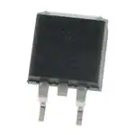
n-channel
D2Pak
TO-262
AUIRG4BC30U-S
AUIRG4BC30U-SL
G
Gate
C
Collector
E
Emitter
Stresses beyond those listed under “Absolute Maximum Ratings” may cause permanent damage to the device.
These are stress ratings only; and functional operation of the device at these or any other condition beyond
those indicated in the specifications is not implied.Exposure to absolute-maximum-rated conditions for
extended periods may affect device reliability. The thermal resistance and power dissipation ratings are
measured under board mounted and still air conditions. Ambient temperature (TA) is 25°C, unless otherwise
specified
Parameter
Max.
Units
VCES
IC @ TC = 25°C
IC @ TC = 100°C
ICM
ILM
VGE
EARV
PD @ TC = 25°C
PD @ TC = 100°C
TJ
TSTG
Collector-to-Emitter Breakdown Voltage
Continuous Collector Current
Continuous Collector Current
Pulsed Collector Current
Clamped Inductive Load Current
Gate-to-Emitter Voltage
Reverse Voltage Avalanche Energy
Maximum Power Dissipation
Maximum Power Dissipation
Operating Junction and
Storage Temperature Range
600
23
12
92
92
± 20
10
100
42
-55 to + 150
V
A
V
mJ
W
°C
Thermal Resistance
Parameter
RθJC
RθJA
Junction-to-Case
Junction-to-Ambient, ( PCB Mounted,steady-state)**
Typ.
Max.
Units
–––
–––
1.2
40
°C/W
* * When mounted on 1" square PCB (FR-4 or G-10 Material ). For recommended footprint and soldering techniques
*
refer to application note #AN-994.
Qualification standards can be found at http://www.irf.com/
www.irf.com
1
11/01/10
�AUIRG4BC30U-S/SL
Dynamic Electrical Characteristics @ TJ = 25°C (unless otherwise specified)
Parameter
Min. Typ. Max. Units
Conditions
Collector-to-Emitter Breakdown Voltage
600
—
—
V
VGE = 0V, IC = 250µA
V(BR)CES
V(BR)ECS
Emitter-to-Collector Breakdown Voltage 18
—
—
V
VGE = 0V, IC = 1.0A
V/°C VGE = 0V, IC = 1.0mA
∆V(BR)CES/∆TJ Temperature Coeff. of Breakdown Voltage — 0.63 —
— 1.95 2.1
IC = 12A
VGE = 15V
VCE(ON)
Collector-to-Emitter Saturation Voltage
— 2.52 —
IC = 23A
See Fig.2, 5
V
— 2.09 —
IC = 12A , TJ = 150°C
VGE(th)
Gate Threshold Voltage
3.0
—
6.0
VCE = VGE, IC = 250µA
∆VGE(th)/∆TJ Temperature Coeff. of Threshold Voltage
—
-13
— mV/°C VCE = VGE, IC = 250µA
gfe
Forward Transconductance
3.1
8.6
—
S
VCE = 100V, IC = 12A
—
—
250
VGE = 0V, VCE = 600V
ICES
Zero Gate Voltage Collector Current
µA
—
—
2.0
VGE = 0V, VCE = 10V, TJ = 25°C
—
— 1000
VGE = 0V, VCE = 600V, TJ = 150°C
IGES
Gate-to-Emitter Leakage Current
—
— ±100
nA
VGE = ±20V
Static or Switching Characteristics @ TJ = 25°C (unless otherwise specified)
Qg
Qge
Qgc
td(on)
tr
td(off)
tf
Eon
Eoff
Ets
td(on)
tr
td(off)
tf
Ets
LE
Cies
Coes
Cres
Parameter
Total Gate Charge (turn-on)
Gate - Emitter Charge (turn-on)
Gate - Collector Charge (turn-on)
Turn-On Delay Time
Rise Time
Turn-Off Delay Time
Fall Time
Turn-On Switching Loss
Turn-Off Switching Loss
Total Switching Loss
Turn-On Delay Time
Rise Time
Turn-Off Delay Time
Fall Time
Total Switching Loss
Internal Source Inductance
Input Capacitance
Output Capacitance
Reverse Transfer Capacitance
Min.
—
—
—
—
—
—
—
—
—
—
—
—
—
—
—
—
—
—
—
Typ.
50
8.1
18
17
9.6
78
97
0.16
0.20
0.36
20
13
180
140
0.73
7.5
1100
73
14
Max. Units
Conditions
75
IC = 12A
12
nC
VCC = 400V
See Fig.8
27
VGE = 15V
—
—
TJ = 25°C
ns
120
IC = 12A, VCC = 480V
150
VGE = 15V, RG = 23Ω
—
Energy losses include "tail"
—
mJ See Fig. 10, 11, 13, 14
0.50
—
TJ = 150°C,
—
IC = 12A, VCC = 480V
ns
—
VGE = 15V, RG = 23Ω
—
Energy losses include "tail"
—
mJ See Fig. 13, 14
—
nH
Measured 5mm from package
—
VGE = 0V
—
pF
VCC = 30V
See Fig.7
—
ƒ = 1.0MHz
Notes:
Repetitive rating; VGE = 20V, pulse width limited by
max. junction temperature. ( See fig. 13b )
VCC = 80%(VCES), VGE = 20V, L = 10µH, RG = 23Ω,
(See fig. 13a)
Pulse width ≤ 80µs; duty factor ≤ 0.1%.
Pulse width 5.0µs, single shot.
Repetitive rating; pulse width limited by maximum
junction temperature.
2
www.irf.com
�AUIRG4BC30U-S/SL
Qualification Information
†
Automotive
(per AEC-Q101)
††
Comments:
This part number(s) passed
Automotive qualification. IR’s Industrial and
Consumer qualification level is granted by
extension of the higher Automotive level.
Qualification Level
Moisture Sensitivity Level
Machine Model
2
D PAK
MSL1
TO-262
N/A
Class M4 (+/-450V)
AEC-Q101-002
ESD
Human Body Model
Class H1C (+/-1750V)
AEC-Q101-001
Charged Device Model
Class C5 (+/-1000V)
AEC-Q101-005
RoHS Compliant
Yes
Qualification standards can be found at International Rectifiers web site: http://www.irf.com
Exceptions to AEC-Q101 requirements are noted in the qualification report.
www.irf.com
3
�AUIRG4BC30U-S/SL
6.0
For both:
5.0
Load Current (A)
Triangular wave:
Duty cycle: 50%
TJ = 125°C
Tsink= 55°C
Gate drive as specified
Power Dissipation = 1.75W
Clamp voltage:
80% of rated
4.0
Square wave:
3.0
60% of rated
voltage
2.0
1.0
Ideal diodes
A
0.0
0.1
1
10
100
f, Frequency (kHz)
Fig. 1 - Typical Load Current vs. Frequency
(For square wave, I=IRMS of fundamental; for triangular wave, I=IPK)
100
TJ = 25°C
TJ = 150°C
10
1
VGE = 15V
20µs PULSE WIDTH A
0.1
0.1
4
1
10
IC , Collector-to-Emitter Current (A)
IC , Collector-to-Emitter Current (A)
100
TJ = 150°C
10
TJ = 25°C
1
V CC = 10V
5µs PULSE WIDTH A
0.1
5
6
7
8
9
10
11
VCE , Collector-to-Emitter Voltage (V)
VGE , Gate-to-Emitter Voltage (V)
Fig. 2 - Typical Output Characteristics
Fig. 3 - Typical Transfer Characteristics
12
www.irf.com
�25
3.0
V GE = 15V
VCE , Collector-to-Emitter Voltage (V)
Maximum DC Collector Current (A
AUIRG4BC30U-S/SL
20
15
10
5
A
0
25
50
75
100
125
V GE = 15V
80µs PULSE WIDTH
IC = 24A
2.5
IC = 12A
2.0
I C = 6.0A
A
1.5
-60
150
-40
-20
0
20
40
60
80
100 120 140 160
TJ , Junction Temperature (°C)
TC , Case Temperature (°C)
Fig. 4 - Maximum Collector Current vs.Case
Temperature
Fig. 5 - Collector-to-Emitter Voltage vs.
Junction Temperature
Thermal Response (Z thJC )
10
1
D = 0.50
0.20
PDM
0.10
0.1
t
0.05
0.02
0.01
SINGLE PULSE
(THERMAL RESPONSE)
Notes:
1. Duty factor D = t
1
/t
1
t2
2
2. Peak TJ = PDM x Z thJC + T C
0.01
0.00001
0.0001
0.001
0.01
0.1
1
10
t 1 , Rectangular Pulse Duration (sec)
Fig. 6 - Maximum Effective Transient Thermal Impedance, Junction-to-Case
www.irf.com
5
�AUIRG4BC30U-S/SL
2000
VGE , Gate-to-Emitter Voltage (V)
1600
C, Capacitance (pF)
20
V GE = 0V,
f = 1MHz
C ies = C ge + C gc , Cce SHORTED
C res = C gc
C oes = C ce + C gc
Cies
1200
800
Coes
400
Cres
16
12
A
0
1
10
VCE = 400V
I C = 12A
8
4
A
0
100
0
10
VCE, Collector-to-Emitter Voltage (V)
10
= 480V
= 15V
= 25°C
= 12A
0.4
0.3
A
0.2
0
10
20
30
40
50
60
R G , Gate Resistance (Ω)
Fig. 9 - Typical Switching Losses vs. Gate
Resistance
6
40
50
Fig. 8 - Typical Gate Charge vs.
Gate-to-Emitter Voltage
Total Switching Losses (mJ)
Total Switching Losses (mJ)
VCC
VGE
TJ
IC
30
Qg , Total Gate Charge (nC)
Fig. 7 - Typical Capacitance vs.
Collector-to-Emitter Voltage
0.5
20
RG = 23 Ω
V GE = 15V
V CC = 480V
IC = 24A
1
I C = 12A
I C = 6.0A
A
0.1
-60
-40
-20
0
20
40
60
80
100 120 140 160
TJ , Junction Temperature (°C)
Fig. 10 - Typical Switching Losses vs.
Junction Temperature
www.irf.com
�AUIRG4BC30U-S/SL
RG
TJ
V CC
V GE
1.2
1000
= 23 Ω
= 150°C
= 480V
= 15V
I C , Collector-to-Emitter Current (A)
Total Switching Losses (mJ)
1.6
0.8
0.4
A
0.0
0
10
20
I C , Collector-to-Emitter Current (A)
Fig. 11 - Typical Switching Losses vs.
Collector-to-Emitter Current
www.irf.com
30
VGE
= 20V
GE
TJ = 125°C
100
SAFE OPERATING AREA
10
1
0.1
1
10
100
1000
VCE , Collector-to-Emitter Voltage (V)
Fig. 12 - Turn-Off SOA
7
�AUIRG4BC30U-S/SL
L
D.U.T.
VC *
50V
RL =
0 - 480V
1000V
c
480V
4 X IC@ 25°C
480µF
960V
d
* Driver same type as D.U.T.; Vc = 80% of Vce(max)
* Note: Due to the 50V power supply, pulse width and inductor
will increase to obtain rated Id.
Fig. 13b - Pulsed Collector
Fig. 13a - Clamped Inductive
Current Test Circuit
Load Test Circuit
IC
L
Driver*
D.U.T.
VC
Test Circuit
50V
1000V
c�
Fig. 14a - Switching Loss
d
e
* Driver same type
as D.U.T., VC = 480V
c
d
90%
e
VC
10%
90%
Fig. 14b - Switching Loss
t d(off)
10%
I C 5%
Waveforms
tf
tr
t d(on)
t=5µs
E on
E off
E ts = (Eon +Eoff )
8
www.irf.com
�AUIRG4BC30U-S/SL
D2Pak (TO-263AB) Package Outline
Dimensions are shown in millimeters (inches)
D2Pak (TO-263AB) Part Marking Information
Part Number
AUG4BC30U-S
YWWA
IR Logo
XX
or
Date Code
Y= Year
WW= Work Week
A= Automotive, Lead Free
XX
Lot Code
Note: For the most current drawing please refer to IR website at http://www.irf.com/package/
www.irf.com
9
�AUIRG4BC30U-S/SL
TO-262 Package Outline
Dimensions are shown in millimeters (inches)
TO-262 Part Marking Information
Part Number
AUG4BC30U-SL
YWWA
IR Logo
XX
or
Date Code
Y= Year
WW= Work Week
A= Automotive, Lead Free
XX
Lot Code
Note: For the most current drawing please refer to IR website at http://www.irf.com/package/
10
www.irf.com
�AUIRG4BC30U-S/SL
D2Pak (TO-263AB) Tape & Reel Information
Dimensions are shown in millimeters (inches)
TRR
1.60 (.063)
1.50 (.059)
4.10 (.161)
3.90 (.153)
FEED DIRECTION 1.85 (.073)
1.65 (.065)
1.60 (.063)
1.50 (.059)
11.60 (.457)
11.40 (.449)
0.368 (.0145)
0.342 (.0135)
15.42 (.609)
15.22 (.601)
24.30 (.957)
23.90 (.941)
TRL
10.90 (.429)
10.70 (.421)
1.75 (.069)
1.25 (.049)
4.72 (.136)
4.52 (.178)
16.10 (.634)
15.90 (.626)
FEED DIRECTION
13.50 (.532)
12.80 (.504)
27.40 (1.079)
23.90 (.941)
4
330.00
(14.173)
MAX.
NOTES :
1. COMFORMS TO EIA-418.
2. CONTROLLING DIMENSION: MILLIMETER.
3. DIMENSION MEASURED @ HUB.
4. INCLUDES FLANGE DISTORTION @ OUTER EDGE.
www.irf.com
60.00 (2.362)
MIN.
26.40 (1.039)
24.40 (.961)
3
30.40 (1.197)
MAX.
4
11
�AUIRG4BC30U-S/SL
Ordering Information
Base part number Package Type
AUIRG4BC30U-SL
AUIRG4BC30U-S
12
TO-262
D2Pak
Standard Pack
Complete Part Number
Form
Quantity
Tube
50
AUIRG4BC30U-SL
Tube
50
AUIRG4BC30U-S
Tape and Reel Left
800
AUIRG4BC30USTRL
Tape and Reel Right
800
AUIRG4BC30USTRR
www.irf.com
�AUIRG4BC30U-S/SL
IMPORTANT NOTICE
Unless specifically designated for the automotive market, International Rectifier Corporation and its subsidiaries (IR) reserve
the right to make corrections, modifications, enhancements, improvements, and other changes to its products and services at
any time and to discontinue any product or services without notice. Part numbers designated with the “AU” prefix follow
automotive industry and / or customer specific requirements with regards to product discontinuance and process change
notification. All products are sold subject to IR’s terms and conditions of sale supplied at the time of order acknowledgment.
IR warrants performance of its hardware products to the specifications applicable at the time of sale in accordance with IR’s
standard warranty. Testing and other quality control techniques are used to the extent IR deems necessary to support this
warranty. Except where mandated by government requirements, testing of all parameters of each product is not necessarily
performed.
IR assumes no liability for applications assistance or customer product design. Customers are responsible for their products
and applications using IR components. To minimize the risks with customer products and applications, customers should
provide adequate design and operating safeguards.
Reproduction of IR information in IR data books or data sheets is permissible only if reproduction is without alteration and is
accompanied by all associated warranties, conditions, limitations, and notices. Reproduction of this information with alterations
is an unfair and deceptive business practice. IR is not responsible or liable for such altered documentation. Information of third
parties may be subject to additional restrictions.
Resale of IR products or serviced with statements different from or beyond the parameters stated by IR for that product or
service voids all express and any implied warranties for the associated IR product or service and is an unfair and deceptive
business practice. IR is not responsible or liable for any such statements.
IR products are not designed, intended, or authorized for use as components in systems intended for surgical implant into the
body, or in other applications intended to support or sustain life, or in any other application in which the failure of the IR product
could create a situation where personal injury or death may occur. Should Buyer purchase or use IR products for any such
unintended or unauthorized application, Buyer shall indemnify and hold International Rectifier and its officers, employees,
subsidiaries, affiliates, and distributors harmless against all claims, costs, damages, and expenses, and reasonable attorney
fees arising out of, directly or indirectly, any claim of personal injury or death associated with such unintended or unauthorized
use, even if such claim alleges that IR was negligent regarding the design or manufacture of the product.
IR products are neither designed nor intended for use in military/aerospace applications or environments unless the IR products
are specifically designated by IR as military-grade or “enhanced plastic.” Only products designated by IR as military-grade
meet military specifications. Buyers acknowledge and agree that any such use of IR products which IR has not designated as
military-grade is solely at the Buyer’s risk, and that they are solely responsible for compliance with all legal and regulatory
requirements in connection with such use.
IR products are neither designed nor intended for use in automotive applications or environments unless the specific IR
products are designated by IR as compliant with ISO/TS 16949 requirements and bear a part number including the designation
“AU”. Buyers acknowledge and agree that, if they use any non-designated products in automotive applications, IR will not be
responsible for any failure to meet such requirements
For technical support, please contact IR’s Technical Assistance Center
http://www.irf.com/technical-info/
WORLD HEADQUARTERS:
233 Kansas St., El Segundo, California 90245
Tel: (310) 252-7105
www.irf.com
13
�


 工商网监
湘ICP备2023018690号
工商网监
湘ICP备2023018690号