July 28, 2017
High Voltage ICs
HIGH SIDE DRIVER IC
AUIRS2123S/AUIRS2124S
Product Summary
Features
Floating channel designed for bootstrap operation
Fully operational to +600 V
Tolerant to negative transient voltage – dV/dt immune
Gate drive supply range from 10 V to 20 V
Undervoltage lockout
CMOS Schmitt-triggered inputs with pull-down
(AUIRS2123S)
CMOS Schmitt-triggered inputs with pull-up
(AUIRS2124S)
Output in phase with input (AUIRS2123S) or out of
Phase with input (AUIRS2124S)
RESET- input is 3.3V and 5V logic compatible
(AUIRS2123S only )
Leadfree, RoHS compliant
Automotive qualified
Topology
Single high side
≤ 600 V
VOFFSET
10 V – 20 V
VOUT
Io+ & I o- (typical)
500 mA
tON & tOFF (typical)
140 ns & 140 ns
Package Options
Typical Applications
General purpose single high side driver
Automotive injection
Automotive inverters
Automotive SMPS
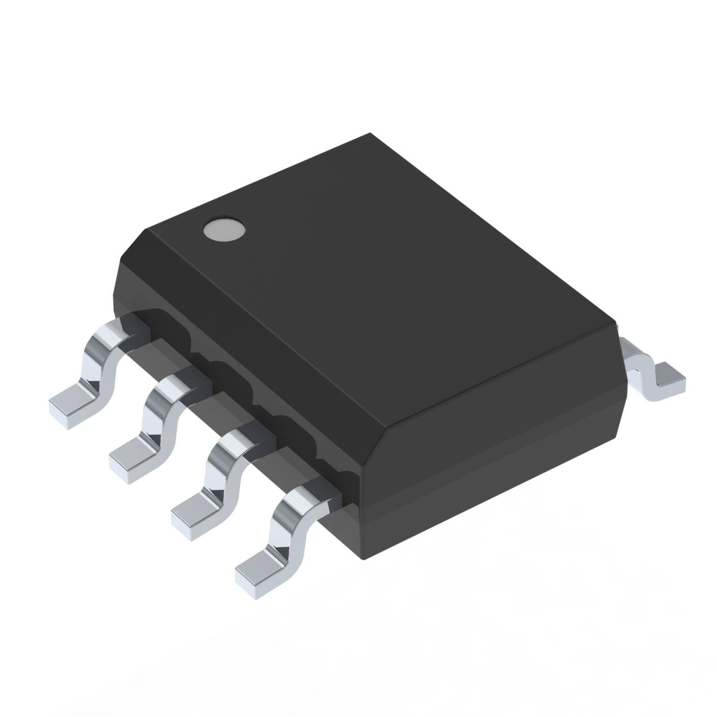
8-Lead SOIC
Typical Connection Diagram
Up to 600 V
Vcc
IN
RESET
Vcc
VB
IN
HO
COM
VS
TO
LOAD
RESET
AUIRS2123S
Up to 600 V
Vcc
IN
(Refer to Lead Assignments for correct pin configuration). This/These
diagram(s) show electrical connections only. Please refer to our
Application Notes and Design Tips for proper circuit board layout.
1
Vcc
VB
IN
HO
COM
VS
TO
LOAD
AUIRS2124S
2017-07-28
�AUIRS2123S
AUIRS2124S
Ordering Information
Standard Pack
Base Part Number
Package Type
Complete Part Number
Form
Quantity
AUIRS2123S
SOIC8
Tape and Reel
2500
AUIRS2123STR
AUIRS2124S
SOIC8
Tape and Reel
2500
AUIRS2124STR
Table of Contents
Page
Description
3
Qualification Information
4
Absolute Maximum Ratings
4
Recommended Operating Conditions
5
Static Electrical Characteristics
6
Dynamic Electrical Characteristics
7
Functional Block Diagram
8
Input/Output Pin Equivalent Circuit Diagram
9
Lead Definitions
10
Lead Assignments
10
Application Information and Additional Details
11
Parameter Temperature Trends
12
Package Details
16
Tape and Reel Details
17
Part Marking Information
18
Publisher notes
2
Rev. 2.1
2017-07-28
2
�AUIRS2123S
AUIRS2124S
Description
The AUIRS2123S/AUIRS2124S are high voltage, high speed power MOSFET and IGBT drivers.
Proprietary HVIC and latch immune CMOS technologies enable ruggedized monolithic construction.
The RESET- input is compatible with standard CMOS outputs (AUIRS2123S only). The output drivers
feature a high pulse current buffer stage designed for minimum cross-conduction.
The floating channel can be used to drive an N-channel power MOSFET or IGBT in the high-side
configuration which operates up to 600 V.
Qualification Information
Qualification Level
Moisture Sensitivity Level
Machine Model
Human Body Model
ESD
Charged Device Model
IC Latch-Up Test
RoHS Compliant
3
Automotive
(per AEC-Q100)
Comments: This family of ICs has passed an Automotive
qualification. IR’s Industrial and Consumer qualification
level is granted by extension of the higher Automotive level.
MSL3 - 260°C
SOIC8
(per IPC/JEDEC J-STD-020)
Class M3
(per AEC-Q100-003)
Class H1C
(per AEC-Q100-002)
Class C5
(per AEC-Q100-011)
Class II, Level A
(per AEC-Q100-004)
Yes
Rev. 2.1
2017-07-28
3
�AUIRS2123S
AUIRS2124S
Absolute Maximum Ratings
Absolute Maximum Ratings indicate sustained limits beyond which damage to the device may occur. All
voltage parameters are absolute voltages referenced to GND, all currents are defined positive into any
lead. This is a stress only rating and operation of the device at these or any conditions exceeding those
indicated in the operational sections of this specification is not implied
Symbol
VBS
VB
VS
VHO
VCC
VIN
VRES
dV/dt
TJ
TS
Definition
High Side Floating Supply Voltage
High Side Driver Output Stage Voltage
High Side Floating Supply Offset Voltage
Output Voltage Gate Connection
Supply Voltage
Input Voltage
Reset Input Voltage
Allowable Offset Voltage Slew Rate
Junction Temperature
Storage Temperature
Min.
-0.3
-0.3
VB - 25
VS – 0.3
-0.3
-0.3
-0.3
-50
-55
-55
Max.
25
625
VB + 0.3
VB + 0.3
25
VCC + 0.3
VCC + 0.3
50
150
150
Units
V
V
V
V
V
V
V
V/nsec
ºC
Recommended Operating Conditions
For proper operations the device should be used within the recommended conditions.
Symbol
Definition
Min.
Max.
High Side Driver Output Stage Voltage
VB
VS +10
VS +20
-10V Transient 0.4 us
High Side Floating Supply Offset Voltage
VS
†
600
-25V Transient 0.4 µs
VS
VB
VHO
Output Voltage Gate Connection
VCC
Supply Voltage
10
20
VIN
VCC
Input Voltage
0
VRES
VCC
Reset Input Voltage
0
Ambient Temperature (fsVccUVLO+
IN
HO
LOW
OFF
LOW
X
OFF
X
X
X
OFF
VBSUVLO+
HIGH
HIGH
ON
很抱歉,暂时无法提供与“AUIRS2123S”相匹配的价格&库存,您可以联系我们找货
免费人工找货