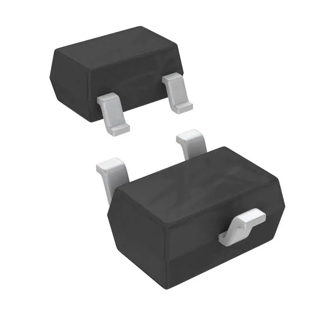
BAR64-04W
Low signal distortion, surface mount RF PIN diode, series pair
Product description
This Infineon cost optimized RF PIN diode is designed for low distortion
switches that require to hold off large RF voltages, and is best suited for
frequencies as high as 3 GHz. Its nominal 50 μm I-region width, combined
with the typical 1.55 μs carrier lifetime, result in a diode with low forward
resistance and low distortion characteristics.
Feature list
•
•
•
•
•
Low signal distortion, charge carrier lifetime trr = 1.55 µs (typical)
Very low capacitance C = 0.25 pF (typical) at voltage VR = 0 and frequencies f ≥ 1 Ghz
Low forward resistance RF = 2.2 Ω (typical) at forward current IF = 10 mA and frequency f = 100 MHz
Industry standard SOT323-3 package (2.1 mm x 2 mm x 0.9 mm)
Pb-free, RoHS compliant and halogen-free
Product validation
Qualified for industrial applications according to the relevant tests of JEDEC47/20/22.
Potential applications
Optimized for low bias current RF and high-speed interface switches and attenuators
• Wireless communication
•
High speed data networks
Device information
Table 1
Part information
Product name / Ordering code
Package
Pin configuration
Marking
Pieces / Reel
BAR64-04W / BAR6404WH6327XTSA1
SOT323-3
Series pair
PPs
3k
Attention: ESD (Electrostatic discharge) sensitive device, observe handling precautions!
Datasheet
www.infineon.com
Please read the Important Notice and Warnings at the end of this document
v1.0
2018-06-30
�BAR64-04W
Low signal distortion, surface mount RF PIN diode, series pair
Table of contents
Table of contents
Product description . . . . . . . . . . . . . . . . . . . . . . . . . . . . . . . . . . . . . . . . . . . . . . . . . . . . . . . . . . . . . . . . . . . . 1
Feature list . . . . . . . . . . . . . . . . . . . . . . . . . . . . . . . . . . . . . . . . . . . . . . . . . . . . . . . . . . . . . . . . . . . . . . . . . . . . . 1
Product validation . . . . . . . . . . . . . . . . . . . . . . . . . . . . . . . . . . . . . . . . . . . . . . . . . . . . . . . . . . . . . . . . . . . . . 1
Potential applications . . . . . . . . . . . . . . . . . . . . . . . . . . . . . . . . . . . . . . . . . . . . . . . . . . . . . . . . . . . . . . . . . . 1
Device information . . . . . . . . . . . . . . . . . . . . . . . . . . . . . . . . . . . . . . . . . . . . . . . . . . . . . . . . . . . . . . . . . . . . . 1
Table of contents . . . . . . . . . . . . . . . . . . . . . . . . . . . . . . . . . . . . . . . . . . . . . . . . . . . . . . . . . . . . . . . . . . . . . . . 2
1
Absolute maximum ratings . . . . . . . . . . . . . . . . . . . . . . . . . . . . . . . . . . . . . . . . . . . . . . . . . . . . . . . . . . . . . .2
2
2.1
2.2
Electrical performance in test fixture . . . . . . . . . . . . . . . . . . . . . . . . . . . . . . . . . . . . . . . . . . . . . . . . . . . . 3
DC characteristics . . . . . . . . . . . . . . . . . . . . . . . . . . . . . . . . . . . . . . . . . . . . . . . . . . . . . . . . . . . . . . . . . . . . . . . 3
AC characteristics . . . . . . . . . . . . . . . . . . . . . . . . . . . . . . . . . . . . . . . . . . . . . . . . . . . . . . . . . . . . . . . . . . . . . . . .4
3
Thermal characteristics . . . . . . . . . . . . . . . . . . . . . . . . . . . . . . . . . . . . . . . . . . . . . . . . . . . . . . . . . . . . . . . . . 9
4
Package information SOT323-3 . . . . . . . . . . . . . . . . . . . . . . . . . . . . . . . . . . . . . . . . . . . . . . . . . . . . . . . . .11
Revision history . . . . . . . . . . . . . . . . . . . . . . . . . . . . . . . . . . . . . . . . . . . . . . . . . . . . . . . . . . . . . . . . . . . . . . . 12
Disclaimer . . . . . . . . . . . . . . . . . . . . . . . . . . . . . . . . . . . . . . . . . . . . . . . . . . . . . . . . . . . . . . . . . . . . . . . . . . . . 13
1
Absolute maximum ratings
Table 2
Absolute maximum ratings at TA = 25 °C, unless otherwise specified
Parameter
Symbol
Values
Min.
Unit
Note or test condition
Max.
Diode reverse voltage
VR
–
150
V
Forward current
IF
–
100
mA
Total power dissipation
PTOT
–
250
mW
Junction temperature
TJ
–
150
°C
Operating temperature
TOP
-55
125
Storage temperature
TSTG
-55
150
TS ≤ 123 °C 1)
Attention: Stresses above the maximum values listed here may cause permanent damage to the device.
Exposure to absolute maximum rating conditions for extended periods may affect device
reliability. Exceeding only one of these values may cause irreversible damage to the component.
1
TS is the soldering point temperature.
Datasheet
2
v1.0
2018-06-30
�BAR64-04W
Low signal distortion, surface mount RF PIN diode, series pair
Electrical performance in test fixture
2
Electrical performance in test fixture
2.1
DC characteristics
At TA = 25 °C, unless otherwise specified
Table 3
DC characteristics
Parameter
Symbol
Values
Min.
Typ.
Max.
Unit
Note or test condition
Breakdown voltage
VBR
150
–
–
V
IR = 5 µA
Reverse current
IR
–
–
20
nA
VR = 20 V
Forward voltage
VF
–
0.82
–
V
IF = 10 mA
–
0.9
–
IF = 50 mA
–
0.95
1.1
IF = 100 mA
–
50
–
I-region width
WI
μm
10 2
I F [mA]
10 1
10 0
10 -1
10 -2
10 -3
0.2
0.4
0.6
0.8
1
1.2
V F [V]
Figure 1
Datasheet
Forward current IF vs. forward voltage VF
3
v1.0
2018-06-30
�BAR64-04W
Low signal distortion, surface mount RF PIN diode, series pair
Electrical performance in test fixture
2.2
AC characteristics
At TA = 25 °C, unless otherwise specified
Table 4
Key parameter
Parameter
Symbol
Capacitance
C
Forward resistance
RF
Values
Unit
Note or test condition
pF
VR = 0 V, f = 1 MHz
Min.
Typ.
Max.
–
0.65
–
–
0.26
0.35
VR = 20 V, f = 1 MHz
–
10.2
20
IF = 1 mA, f = 100 MHz
–
4.4
–
IF = 3 mA, f = 100 MHz
–
3.2
–
IF = 5 mA, f = 100 MHz
–
2.2
2.8
IF = 10 mA, f = 100 MHz
–
–
1.35
IF = 100 mA, f = 100 MHz
Inductance
Ls
–
1.4
–
nH
Charge carrier lifetime
τrr
–
1550
–
ns
IF = 10 mA, IR = 6 mA,
measured at IR = 3 mA,
RL = 100 Ω
Unit
Note or test condition
Table 5
AC parameter at f = 1 GHz
Parameter
Symbol
Values
Min.
Typ.
Max.
Capacitance
C
–
0.23
–
pF
VR = 0 V
Reverse parallel resistance
RP
–
3.5
–
kΩ
VR = 0 V
Forward resistance
RF
–
10.2
–
Ω
IF = 1 mA
–
4.4
–
IF = 3 mA
–
3.3
–
IF = 5 mA
–
2.4
–
IF = 10 mA
–
0.84
–
–
0.41
–
IF = 3 mA
–
0.31
–
IF = 5 mA
–
0.24
–
IF = 10 mA
–
18.6
–
VR = 0 V
Insertion loss
IL
Isolation
Table 6
ISO
dB
IF = 1 mA
AC parameter at f = 1.8 GHz
Parameter
Symbol
Values
Min.
Typ.
Max.
Unit
Note or test condition
Capacitance
C
–
0.23
–
pF
VR = 0 V
Reverse parallel resistance
RP
–
2.8
–
kΩ
VR = 0 V
Datasheet
4
v1.0
2018-06-30
�BAR64-04W
Low signal distortion, surface mount RF PIN diode, series pair
Electrical performance in test fixture
Table 6
AC parameter at f = 1.8 GHz (continued)
Parameter
Symbol
Forward resistance
RF
Insertion loss
IL
Isolation
Table 7
ISO
Values
Unit
Note or test condition
Ω
IF = 1 mA
Min.
Typ.
Max.
–
10.2
–
–
4.5
–
IF = 3 mA
–
3.4
–
IF = 5 mA
–
2.5
–
IF = 10 mA
–
0.89
–
–
0.46
–
IF = 3 mA
–
0.37
–
IF = 5 mA
–
0.29
–
IF = 10 mA
–
13.7
–
VR = 0 V
dB
IF = 1 mA
AC parameter at f = 2.5 GHz
Parameter
Symbol
Values
Min.
Typ.
Max.
Unit
Note or test condition
Capacitance
C
–
0.23
–
pF
VR = 0 V
Reverse parallel resistance
RP
–
2.5
–
kΩ
VR = 0 V
Forward resistance
RF
–
10.2
–
Ω
IF = 1 mA
–
4.7
–
IF = 3 mA
–
3.5
–
IF = 5 mA
–
2.6
–
IF = 10 mA
–
0.94
–
–
0.53
–
IF = 3 mA
–
0.43
–
IF = 5 mA
–
0.36
–
IF = 10 mA
–
11
–
VR = 0 V
Insertion loss
Isolation
Datasheet
IL
ISO
5
dB
IF = 1 mA
v1.0
2018-06-30
�BAR64-04W
Low signal distortion, surface mount RF PIN diode, series pair
Electrical performance in test fixture
0.6
0.5
C [pF]
0.4
1 MHz
1...3 GHz
0.3
0.2
0.1
0
5
10
15
20
25
30
35
40
VR [V]
Figure 2
Capacitance C vs. reverse voltage VR at different frequencies
Figure 3
Reverse parallel resistance RP vs. reverse voltage VR at different frequencies
Datasheet
6
v1.0
2018-06-30
�BAR64-04W
Low signal distortion, surface mount RF PIN diode, series pair
Electrical performance in test fixture
Figure 4
Forward resistance RF vs. forward current IF at different frequencies
0
-0.2
I L [dB]
-0.4
100 mA
10 mA
5 mA
3 mA
1 mA
-0.6
-0.8
-1
0
1
2
3
4
5
6
f [GHz]
Figure 5
Datasheet
Insertion loss IL vs. frequency f at different forward currents
7
v1.0
2018-06-30
�BAR64-04W
Low signal distortion, surface mount RF PIN diode, series pair
Electrical performance in test fixture
0
-5
I SO [dB]
-10
-15
-20
0V
1V
10 V
-25
-30
-35
0
1
2
3
4
5
6
f [GHz]
Figure 6
Note:
Datasheet
Isolation ISO vs. frequency f at different reverse voltages
The curves shown in this chapter have been generated using typical devices but shall not be
understood as a guarantee that all devices have identical characteristic curves.
8
v1.0
2018-06-30
�BAR64-04W
Low signal distortion, surface mount RF PIN diode, series pair
Thermal characteristics
3
Thermal characteristics
Table 8
Thermal resistance
Parameter
Sym
bol
Thermal resistance
(junction - soldering point)
RthJS
Values
Min.
Typ.
Max.
–
105
–
Unit
Note or test condition
K/W
TS = 123 °C 2)
120
100
I F [mA]
80
60
40
20
0
0
20
40
60
80
100
120
140
160
T S [°C]
Figure 7
2
Permissible forward current IF in DC operation
For RthJS in other conditions refer to the curves in this chapter.
Datasheet
9
v1.0
2018-06-30
�BAR64-04W
Low signal distortion, surface mount RF PIN diode, series pair
Thermal characteristics
Figure 8
Thermal resistance RthJS in pulse operation
Figure 9
Permissible forward current ratio IFmax/IDC in pulse operation
Datasheet
10
v1.0
2018-06-30
�BAR64-04W
Low signal distortion, surface mount RF PIN diode, series pair
Package information SOT323-3
Package information SOT323-3
A
0.15 -0.05
+0.10
1.25 ±0.1
0.9 ±0.1
4
0.1 MAX.
0.1
0.1 MIN.
2.1 ±0.1
A
+0.10
0.3 -0.05
3
0.65 0.65
2
2 ±0.2
1
0.1
3x
0.2
MOLD FLAS H, P ROTRUS ION OR GATE BURRS OF 0.2 MM MAXIMUM P ER S IDE ARE NOT INCLUDED
ALL DIMENS IONS ARE IN UNITS MM
THE DRAWING IS IN COMP LIANCE WITH IS O 128 & P ROJ ECTION METHOD 1 [
]
Figure 10
Package outline
Figure 11
Foot print
TYP E CODE
NOTE OF MANUFACTURER
MONTH
YEAR
Figure 12
Marking layout example
4
0.2
P IN 1
INDEX MARKING
2.3
1.9
8
2
2.15
ALL DIMENS IONS ARE IN UNITS MM
THE DRAWING IS IN COMP LIANCE WITH IS O 128 & P ROJ ECTION METHOD 1 [
Figure 13
Datasheet
1.1
]
Tape information
11
v1.0
2018-06-30
�BAR64-04W
Low signal distortion, surface mount RF PIN diode, series pair
Revision history
Revision history
Document
version
Date of
release
Description of changes
1.0
2018-09-07
•
•
•
•
•
1.1
Datasheet
2019-01-21
Change from series datasheet to individual one
Initial release of datasheet
Typical values and curves updated to the values of the production
(No product or process change behind)
Maximum/typical values added
Typical curves/values removed
Product description, feature list and potential application section reworked
12
v1.0
2018-06-30
�Trademarks
All referenced product or service names and trademarks are the property of their respective owners.
Edition 2018-06-30
Published by
Infineon Technologies AG
81726 Munich, Germany
© 2019 Infineon Technologies AG
All Rights Reserved.
Do you have a question about any
aspect of this document?
Email: erratum@infineon.com
Document reference
IFX-zsj1535451723248
IMPORTANT NOTICE
The information given in this document shall in no
event be regarded as a guarantee of conditions or
characteristics (“Beschaffenheitsgarantie”) .
With respect to any examples, hints or any typical values
stated herein and/or any information regarding the
application of the product, Infineon Technologies
hereby disclaims any and all warranties and liabilities of
any kind, including without limitation warranties of
non-infringement of intellectual property rights of any
third party.
In addition, any information given in this document is
subject to customer’s compliance with its obligations
stated in this document and any applicable legal
requirements, norms and standards concerning
customer’s products and any use of the product of
Infineon Technologies in customer’s applications.
The data contained in this document is exclusively
intended for technically trained staff. It is the
responsibility of customer’s technical departments to
evaluate the suitability of the product for the intended
application and the completeness of the product
information given in this document with respect to such
application.
WARNINGS
Due to technical requirements products may contain
dangerous substances. For information on the types
in question please contact your nearest Infineon
Technologies office.
Except as otherwise explicitly approved by Infineon
Technologies in a written document signed by
authorized representatives of Infineon Technologies,
Infineon Technologies’ products may not be used in
any applications where a failure of the product or
any consequences of the use thereof can reasonably
be expected to result in personal injury
�