BAR67...
Silicon PIN Diode
• For low loss RF switches and attenuators
• Very low capacitance at zero volt reverse
bias at frequencies above 1 GHz (typ. 0.25 pF)
• Low forward resistance (typ. 1.5 Ω @ 5mA)
• Low harmonics
• Pb-free (RoHS compliant) package
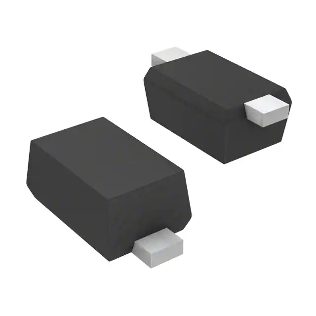
BAR67-02V
BAR67-04
!
�
, �
,
�
Type
BAR67-02V
BAR67-04
Package
SC79
SOT23
Configuration
single
series
LS(nH)
0.6
1.8
Marking
T
PMs
Maximum Ratings at TA = 25°C, unless otherwise specified
Parameter
Symbol
Value
Unit
Diode reverse voltage
VR
150
V
Forward current
IF
200
mA
Total power dissipation
Ptot
mW
TS ≤ 118°C, BAR67-02V
250
TS ≤ 25°C, BAR67-04
250
150
Junction temperature
Tj
Operating temperature range
Top
-55 ... 125
Storage temperature
Tstg
-55 ... 150
°C
Thermal Resistance
Parameter
Symbol
Junction - soldering point1)
RthJS
Value
K/W
BAR67-02V
≤ 115
BAR67-04
≤ 290
1For
Unit
calculation of RthJA please refer to Application Note Thermal Resistance
1
2011-06-14
�BAR67...
Electrical Characteristics at TA = 25°C, unless otherwise specified
Symbol
Parameter
Values
Unit
min.
typ.
max.
150
-
-
V
IR
-
-
20
nA
VF
-
0.95
1.2
V
DC Characteristics
Breakdown voltage
V(BR)
I(BR) = 5 µA
Reverse current
VR = 100 V
Forward voltage
IF = 50 mA
AC Characteristics
Diode capacitance
pF
CT
VR = 5 V, f = 1 MHz
-
0.35
0.55
VR = 0 V, f = 100 MHz
-
0.35
0.9
VR = 0 V, f = 1 GHz
-
0.25
-
VR = 0 V, f = 1.8 GHz
-
0.23
-
Reverse parallel resistance
RP
kΩ
VR = 0 V, f = 100 MHz
-
25
-
VR = 0 V, f = 1 GHz
-
4
-
VR = 0 V, f = 1.8 GHz
-
2.5
-
Forward resistance
Ω
rf
IF = 5 mA, f = 100 MHz
-
1.5
1.8
IF = 10 mA, f = 100 MHz
-
1
-
τ rr
-
700
-
ns
WI
-
13
-
µm
Charge carrier life time
IF = 10 mA, IR = 6 mA, measured at IR = 3 mA,
RL = 100 Ω
I-region width
2
2011-06-14
�BAR67...
Diode capacitance CT = ƒ (VR)
Reverse parallel resistance RP = ƒ(VR)
f = Parameter
f = Parameter
10 4
0.5
KOhm
F
10 3
1 MHz
100 MHz
1 GHz
1.8 GHz
0.35
Rp
CT
0.4
100 MHz
10 2
0.3
1 GHz
10 1
0.25
1.8 GHz
0.2
10 0
0.15
0.1
0
5
10
15
20
25
V
30
10 -1
0
40
5
10
15
20
25
V
30
VR
40
VR
Forward resistance rf = ƒ (IF)
Forward current IF = ƒ (VF)
f = 100MHz
TA = Parameter
10 3
10 0
A
Ohm
10 -1
10 2
rf
IF
10 -2
10 1
10 -3
-40 °C
25 °C
85 °C
125 °C
10 -4
10 0
10 -5
10 -1 -2
10
10
-1
10
0
10
1
mA 10
10 -6
0
2
IF
0.2
0.4
0.6
0.8
V
1.2
VF
3
2011-06-14
�BAR67...
Forward current IF = ƒ (TS )
Forward current IF = ƒ (TS )
BAR67-02V
BAR67-04
250
220
mA
mA
180
200
160
IF
IF
175
150
140
120
125
100
100
80
75
60
50
40
25
0
0
20
15
30
45
60
90 105 120 °C
75
0
0
150
20
40
60
80
120 °C
100
TS
150
TS
Permissible Puls Load RthJS = ƒ (t p)
Permissible Pulse Load
BAR67-02V
IFmax/ IFDC = ƒ (t p)
BAR67-02V
10 3
10 2
IFmax/IFDC
K/W
RthJS
10 2
10
D=0.5
0.2
0.1
0.05
0.02
0.01
0.005
0
1
10 0
10 -1 -6
10
10
-5
10
-4
10
-3
D=0
0.005
0.01
0.02
0.05
0.1
0.2
0.5
10 1
10
-2
s
10
10 0 -6
10
0
tP
10
-5
10
-4
10
-3
10
-2
s
10
0
tP
4
2011-06-14
�BAR67...
Permissible Puls Load RthJS = ƒ (t p)
BAR67-04
10 3
K/W
RthJS
10 2
10 1
0.5
0.2
0.1
0.05
0.02
0.01
0.005
D=0
10 0
10 -1 -6
10
10
-5
10
-4
10
-3
10
-2
s
10
0
tP
5
2011-06-14
�Package SC79
6
BAR67...
2011-06-14
�BAR67...
Date Code marking for discrete packages with
one digit (SCD80, SC79, SC75 1) ) CES-Code
Month 2 0 03
2 0 04
2005
2006
2 0 07
2008
2009
2010
2011
2012
2 0 13
2014
01
a
p
A
P
a
p
A
P
a
p
A
P
02
b
q
B
Q
b
q
B
Q
b
q
B
Q
03
c
r
C
R
c
r
C
R
c
r
C
R
04
d
s
D
S
d
s
D
S
d
s
D
S
05
e
t
E
T
e
t
E
T
e
t
E
T
06
f
u
F
U
f
u
F
U
f
u
F
U
07
g
v
G
V
g
v
G
V
g
v
G
V
08
h
x
H
X
h
x
H
X
h
x
H
X
09
j
y
J
Y
j
y
J
Y
j
y
J
Y
10
k
z
K
Z
k
z
K
Z
k
z
K
Z
11
l
2
L
4
l
2
L
4
l
2
L
4
12
n
3
N
5
n
3
N
5
n
3
N
5
1) New Marking Layout for SC75, implemented at October 2005.
.
7
2011-06-14
�Package SOT23
BAR67...
0.4 +0.1
-0.05
1)
2
0.08...0.1
C
0.95
1.3 ±0.1
1
2.4 ±0.15
3
0.1 MAX.
10˚ MAX.
B
1 ±0.1
10˚ MAX.
2.9 ±0.1
0.15 MIN.
Package Outline
A
5
0...8˚
1.9
0.2
0.25 M B C
M
A
1) Lead width can be 0.6 max. in dambar area
Foot Print
0.8
0.9
1.3
0.9
0.8
1.2
Marking Layout (Example)
Manufacturer
EH s
2005, June
Date code (YM)
Pin 1
BCW66
Type code
Standard Packing
Reel ø180 mm = 3.000 Pieces/Reel
Reel ø330 mm = 10.000 Pieces/Reel
4
0.2
8
2.13
2.65
0.9
Pin 1
1.15
3.15
8
2011-06-14
�BAR67...
Edition 2009-11-16
Published by
Infineon Technologies AG
81726 Munich, Germany
2009 Infineon Technologies AG
All Rights Reserved.
Legal Disclaimer
The information given in this document shall in no event be regarded as a guarantee
of conditions or characteristics. With respect to any examples or hints given herein,
any typical values stated herein and/or any information regarding the application of
the device, Infineon Technologies hereby disclaims any and all warranties and
liabilities of any kind, including without limitation, warranties of non-infringement of
intellectual property rights of any third party.
Information
For further information on technology, delivery terms and conditions and prices,
please contact the nearest Infineon Technologies Office ().
Warnings
Due to technical requirements, components may contain dangerous substances.
For information on the types in question, please contact the nearest Infineon
Technologies Office.
Infineon Technologies components may be used in life-support devices or systems
only with the express written approval of Infineon Technologies, if a failure of such
components can reasonably be expected to cause the failure of that life-support
device or system or to affect the safety or effectiveness of that device or system.
Life support devices or systems are intended to be implanted in the human body or
to support and/or maintain and sustain and/or protect human life. If they fail, it is
reasonable to assume that the health of the user or other persons may be
endangered.
9
2011-06-14
�
很抱歉,暂时无法提供与“BAR6702VH6327XTSA1”相匹配的价格&库存,您可以联系我们找货
免费人工找货- 国内价格
- 5+1.81635
- 50+1.44299
- 150+1.28294
- 500+1.08324
- 3000+0.94997
- 6000+0.89651