BGA123L4
BGA123L4
Sma ll Footprint Ultra Low Curren t Low Noise Amplifier for Global
Navigation Satellite Systems ( GNSS)
Features
•
Operating frequencies: 1550 - 1615 MHz
•
Ultra low current consumption: 1.1 mA
•
Wide supply voltage range: 1.1 V to 3.6 V
•
High insertion power gain: 18.2 dB
•
Low noise figure: 0.75 dB
•
2 kV HBM ESD protection (including AI pin)
•
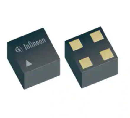
Ultra small TSLP-4-11 leadless package (footprint: 0.7 x 0.7 x 0.31
mm3)
•
RF output internally matched to 50 Ohm
•
Only one external SMD compenent necessary
•
Pb-free (RoHS complaint) package
0.7 x 0.7 x 0.31 mm³
Application
BGA123L4 is designed to enhance GNSS signal sensitivity especially in wearables and mobile cellular IoT devices.
With 18.2 dB gain and only 0.75 dB noise figure it ensures high system sensitivity. The current needed is only 1.1
mA which means just 1.3 mW power consumption, which is critical to help to conserve batteries. The wide supply
voltage range of 1.1 V to 3.6 V ensures flexible design and high compatibility. It supports all GNSS systems
including GPS, GLONASS, Beidou and Galileo.
Product Validation
Qualified for industrial applications according to the relevant tests of JEDEC47/20/22.
Block diagram
VCC
AI
AO
ESD
GND
BGA123L4_Blockdiagram.vsd
Data Sheet
www.infineon.com
Revision 2.0 (min/max)
2017-09-14
�BGA123L4
Small Footprint Ultra Low Current Low Noise Amplifier for Global Navigation
Table of Contents
Table of Contents
Table of Contents . . . . . . . . . . . . . . . . . . . . . . . . . . . . . . . . . . . . . . . . . . . . . . . . . . . . . . . . . . . . . . . . . . 2
1
Features . . . . . . . . . . . . . . . . . . . . . . . . . . . . . . . . . . . . . . . . . . . . . . . . . . . . . . . . . . . . . . . . . . . . . . . . . 3
2
Maximum Ratings . . . . . . . . . . . . . . . . . . . . . . . . . . . . . . . . . . . . . . . . . . . . . . . . . . . . . . . . . . . . . . . . . 5
3
Electrical Characteristics . . . . . . . . . . . . . . . . . . . . . . . . . . . . . . . . . . . . . . . . . . . . . . . . . . . . . . . . . . . 6
4
Application Information . . . . . . . . . . . . . . . . . . . . . . . . . . . . . . . . . . . . . . . . . . . . . . . . . . . . . . . . . . . . 9
5
Package Information . . . . . . . . . . . . . . . . . . . . . . . . . . . . . . . . . . . . . . . . . . . . . . . . . . . . . . . . . . . . . . 10
Data Sheet
2
Revision 2.0 (min/max)
2017-09-14
�BGA123L4
Small Footprint Ultra Low Current Low Noise Amplifier for Global Navigation
Features
1
Features
•
Operating frequencies: 1550 - 1615 MHz
•
Ultra low current consumption: 1.1 mA
•
Wide supply voltage range: 1.1 V to 3.6 V
•
High insertion power gain: 18.2 dB
•
Low noise figure: 0.75 dB
•
2 kV HBM ESD protection (including AI pin)
•
Ultra small TSLP-4-11 leadless package (footprint: 0.7 x 0.7 x 0.31
mm3)
•
RF output internally matched to 50 Ohm
•
Only one external SMD compenent necessary
•
Pb-free (RoHS complaint) package
•
B7HF Silicon Germanium technology
VCC
AI
AO
ESD
GND
BGA123L4_Blockdiagram.vsd
Figure 1
Block Diagram
Product Name
Marking
Package
BGA123L4
B
TSLP-4-11
Data Sheet
3
Revision 2.0 (min/max)
2017-09-14
�BGA123L4
Small Footprint Ultra Low Current Low Noise Amplifier for Global Navigation
Features
Description
The BGA123L4 is a ultra low current low noise amplifier for Global Navigation Satellite Systems (GNSS) which
covers all GNSS frequency bands from 1550 MHz to 1615 MHz like GPS, GLONASS, Beidou, Galileo and others. The
LNA provides 18.2 dB gain and 0.75 dB noise figure at a current consumption of only 1.1 mA in the application
configuration described in Chapter 4. The BGA123L4 is based upon Infineon Technologies‘ B7HF Silicon
Germanium technology. It operates from 1.1 V to 3.6 V supply voltage.
Pin Definition and Function
Table 1
Pin Definition and Function
Pin No.
Name
Function
1
VCC
DC supply
2
AO
LNA output
3
GND
Ground
4
AI
LNA input
Data Sheet
4
Revision 2.0 (min/max)
2017-09-14
�BGA123L4
Small Footprint Ultra Low Current Low Noise Amplifier for Global Navigation
Maximum Ratings
2
Maximum Ratings
Table 2
Maximum Ratings
Parameter
Symbol
Values
Min.
Typ.
Max.
Unit
Note or
Test Condition
Voltage at pin VCC
VCC
-0.3
–
3.6
V
1)
Voltage at pin AI
VAI
-0.3
–
0.9
V
–
Voltage at pin AO
VAO
-0.3
–
VCC + 0.3
V
–
Voltage at pin GND
VGND
-0.3
–
0.3
V
–
Current into pin VCC
ICC
–
–
10
mA
–
RF input power
PIN
–
–
0
dBm
–
Total power dissipation,
TS < 148 °C2)
Ptot
–
–
40
mW
–
Junction temperature
TJ
–
–
150
°C
–
Ambient temperature range
TA
-40
–
85
°C
–
Storage temperature range
TSTG
-65
–
150
°C
–
ESD capability all pins
VESD_HBM
-2000
–
2000
V
according to
JS-001
1) All voltages refer to GND-Node unless otherwise noted
2) TS is measured on the ground lead at the soldering point
Attention: Stresses above the max. values listed here may cause permanent damage to the device.
Maximum ratings are absolute ratings; exceeding only one of these values may cause
irreversible damage to the integrated circuit. Exposure to conditions at or below absolute
maximum rating but above the specified maximum operation conditions may affect device
reliability and life time. Functionality of the device might not be given under these conditions.
Data Sheet
5
Revision 2.0 (min/max)
2017-09-14
�BGA123L4
Small Footprint Ultra Low Current Low Noise Amplifier for Global Navigation
Electrical Characteristics
3
Electrical Characteristics
Table 3
Electrical Characteristics1)
TA = 25 °C, VCC = 1.2 V, f = 1550 - 1615 MHz
Parameter
Supply voltage
Supply current
Symbol
VCC
ICC
2
Values
Unit
Note or Test Condition
Min.
Typ.
Max.
1.1
1.8
3.6
V
ON-Mode
0.0
–
0.4
V
OFF-Mode
–
1.05
1.55
mA
ON-Mode, Vcc=1.2V
–
0.1
2
µA
OFF-Mode
Insertion power gain
f = 1575 MHz
|S21|
16.4
17.9
19.4
dB
ON-Mode
Noise figure2)
f = 1575 MHz, ZS = 50 Ω
NF
–
0.75
1.25
dB
ON-Mode, ZS = 50 Ω
Input return loss3)
f = 1575 MHz
RLIN
7
9
–
dB
ON-Mode
Output return loss3)
f = 1575 MHz
RLOUT
10
16
–
dB
ON-Mode
Reverse isolation3)
f = 1575 MHz
1/|S12|2
25
36
–
dB
ON-Mode
Transient time4)7)
tS
–
0.5
2
µs
ON- to OFF-Mode
–
9
12
µs
OFF- to ON-Mode
Inband input 1dB-compression IP1dB
point, f = 1575 MHz3)
-21
-17
–
dBm
ON-Mode
Inband input 3rd-order
intercept point3)5)
f1 = 1575 MHz, f2 = f1 +/- 1 MHz
-19
-14
–
dBm
ON-Mode
Out of band input 3rd-order
OOB-IIP3
intercept
point3)6)f1 = 1713 MHz, f2 = 1851
MHz
-14
-9
–
dBm
ON-Mode
Stability7)
>1
–
–
1)
2)
3)
4)
5)
6)
7)
IIP3
k
f = 20 MHz ... 10 GHz
Based on the application described in chapter 4
PCB losses are subtracted
Verification based on AQL; not 100% tested in production
To be within 1 dB of the final gain
Input power = -30 dBm for each tone
Input power = -20 dBm at f1 and -65 dBm at f2
Guaranteed by device design; not tested in production
Data Sheet
6
Revision 2.0 (min/max)
2017-09-14
�BGA123L4
Small Footprint Ultra Low Current Low Noise Amplifier for Global Navigation
Electrical Characteristics
Table 4
Electrical Characteristics1)
TA = 25 °C, VCC = 1.8 V, f = 1550 - 1615 MHz
Parameter
Supply voltage
Supply current
Symbol
VCC
ICC
2
Values
Unit
Note or Test Condition
Min.
Typ.
Max.
1.1
1.8
3.6
V
ON-Mode
0.0
–
0.4
V
OFF-Mode
–
1.1
1.6
mA
ON-Mode, Vcc=1.8V
–
0.1
2
µA
OFF-Mode
Insertion power gain
f = 1575 MHz
|S21|
16.7
18.2
19.7
dB
ON-Mode
Noise figure2)
f = 1575 MHz, ZS = 50 Ω
NF
–
0.75
1.25
dB
ON-Mode, ZS = 50 Ω
Input return loss3)
f = 1575 MHz
RLIN
7
9
–
dB
ON-Mode
Output return loss3)
f = 1575 MHz
RLOUT
10
16
–
dB
ON-Mode
Reverse isolation3)
f = 1575 MHz
1/|S12|2
25
36
–
dB
ON-Mode
Transient time4)7)
tS
–
0.5
2
µs
ON- to OFF-Mode
–
6
9
µs
OFF- to ON-Mode
Inband input 1dB-compression IP1dB
point, f = 1575 MHz3)
-19
-15
–
dBm
ON-Mode
Inband input 3rd-order
intercept point3)5)
f1 = 1575 MHz, f2 = f1 +/- 1 MHz
-19
-14
–
dBm
ON-Mode
Out of band input 3rd-order
OOB-IIP3
intercept
point3)6)f1 = 1713 MHz, f2 = 1851
MHz
-14
-9
–
dBm
ON-Mode
Stability7)
>1
–
–
1)
2)
3)
4)
5)
6)
7)
IIP3
k
f = 20 MHz ... 10 GHz
Based on the application described in chapter 4
PCB losses are subtracted
Verification based on AQL; not 100% tested in production
To be within 1 dB of the final gain
Input power = -30 dBm for each tone
Input power = -20 dBm at f1 and -65 dBm at f2
Guaranteed by device design; not tested in production
Data Sheet
7
Revision 2.0 (min/max)
2017-09-14
�BGA123L4
Small Footprint Ultra Low Current Low Noise Amplifier for Global Navigation
Electrical Characteristics
Table 5
Electrical Characteristics1)
TA = 25 °C, VCC = 2.8 V, f = 1550 - 1615 MHz
Parameter
Supply voltage
Supply current
Symbol
VCC
ICC
2
Values
Unit
Note or Test Condition
Min.
Typ.
Max.
1.1
1.8
3.6
V
ON-Mode
0.0
–
0.4
V
OFF-Mode
–
1.2
1.7
mA
ON-Mode, Vcc=2.8V
–
0.1
2
µA
OFF-Mode
Insertion power gain
f = 1575 MHz
|S21|
16.9
18.4
19.9
dB
ON-Mode
Noise figure2)
f = 1575 MHz, ZS = 50 Ω
NF
–
0.75
1.25
dB
ON-Mode, ZS = 50 Ω
Input return loss3)
f = 1575 MHz
RLIN
7
9
–
dB
ON-Mode
Output return loss3)
f = 1575 MHz
RLOUT
10
15
–
dB
ON-Mode
Reverse isolation3)
f = 1575 MHz
1/|S12|2
25
36
–
dB
ON-Mode
Transient time4)7)
tS
–
0.5
2
µs
ON- to OFF-Mode
–
5
8
µs
OFF- to ON-Mode
Inband input 1dB-compression IP1dB
point, f = 1575 MHz3)
-17
-13
–
dBm
ON-Mode
Inband input 3rd-order
intercept point3)5)
f1 = 1575 MHz, f2 = f1 +/- 1 MHz
-19
-14
–
dBm
ON-Mode
Out of band input 3rd-order
OOB-IIP3
intercept
point3)6)f1 = 1713 MHz, f2 = 1851
MHz
-14
-9
–
dBm
ON-Mode
Stability7)
>1
–
–
1)
2)
3)
4)
5)
6)
7)
IIP3
k
f = 20 MHz ... 10 GHz
Based on the application described in chapter 4
PCB losses are subtracted
Verification based on AQL; not 100% tested in production
To be within 1 dB of the final gain
Input power = -30 dBm for each tone
Input power = -20 dBm at f1 and -65 dBm at f2
Guaranteed by device design; not tested in production
Data Sheet
8
Revision 2.0 (min/max)
2017-09-14
�BGA123L4
Small Footprint Ultra Low Current Low Noise Amplifier for Global Navigation
Application Information
4
Application Information
Application Board Configuration
N1 BGA123L4
GND
AO, 2
GND, 3
RFout
L1
C1
RFin
VCC
VCC, 1
AI, 4
C2
BGA123L4_Schematic.vsd
Figure 2
Application Schematic BGA123L4
Table 6
Bill of Materials
Name
Value
Package
Manufacturer
Function
C1 (optional)
1nF
0402
Various
DC block1)
C2
≥ 1nF2)
0402
Various
RF bypass 3)
L1
10nH
0402
Murata LQW15 type
Input matching
N1
BGA123L4
TSLP-4-11
Infineon
SiGe LNA
1) DC block might be realized with pre-filter in GNSS applications
2) For data sheet charcteristics 1nF used
3) RF bypass recommended to mitigate power supply noise
A list of all application notes is available at http://www.infineon.com/gpslna.appnotes
Data Sheet
9
Revision 2.0 (min/max)
2017-09-14
�BGA123L4
Small Footprint Ultra Low Current Low Noise Amplifier for Global Navigation
Package Information
5
Package Information
TSLP-4-11-PO.vsd
Figure 3
TSLP-4-11 Package Outline (top, side and bottom views)
0.25
0.4
0.4
Copper
0.4
0.4
0.25
0.25
Optional solder
mask dam
Stencil apertures
Solder mask
TSLP-4-11-FP V01
Footprint Recommendation TSLP-4-11
1
Figure 4
Pin 1 marking
Type code
Date code (M)
TSLP-4-11-MK V01
Figure 5
Data Sheet
Marking Layout (top view)
10
Revision 2.0 (min/max)
2017-09-14
�BGA123L4
Small Footprint Ultra Low Current Low Noise Amplifier for Global Navigation
Package Information
Figure 6
Data Sheet
Tape & Reel Dimensions (reel diameter 180 mm, pieces/reel 15000)
11
Revision 2.0 (min/max)
2017-09-14
�BGA123L4
Small Footprint Ultra Low Current Low Noise Amplifier for Global Navigation
Revision History
Page or Item
Subjects (major changes since previous revision)
Revision 2.0 (min/max), 2017-09-14
1, 3, 4, 6, 7 , 8
Update Electrical Characteristics
13
Update Trademark Information
Data Sheet
12
Revision 2.0 (min/max)
2017-09-14
�Please read the Important Notice and Warnings at the end of this document
Other Trademarks
All referenced product or service names and trademarks are the property of their respective owners.
Edition 2017-09-14
Published by
Infineon Technologies AG
81726 Munich, Germany
© 2017 Infineon Technologies AG.
All Rights Reserved.
Do you have a question about any
aspect of this document?
Email: erratum@infineon.com
Document reference
Doc_Number
IMPORTANT NOTICE
The information given in this document shall in no
event be regarded as a guarantee of conditions or
characteristics ("Beschaffenheitsgarantie").
With respect to any examples, hints or any typical
values stated herein and/or any information regarding
the application of the product, Infineon Technologies
hereby disclaims any and all warranties and liabilities
of any kind, including without limitation warranties of
non-infringement of intellectual property rights of any
third party.
In addition, any information given in this document is
subject to customer's compliance with its obligations
stated in this document and any applicable legal
requirements, norms and standards concerning
customer's products and any use of the product of
Infineon Technologies in customer's applications.
The data contained in this document is exclusively
intended for technically trained staff. It is the
responsibility of customer's technical departments to
evaluate the suitability of the product for the intended
application and the completeness of the product
information given in this document with respect to
such application.
For further information on technology, delivery terms
and conditions and prices, please contact the nearest
Infineon Technologies Office (www.infineon.com).
WARNINGS
Due to technical requirements products may contain
dangerous substances. For information on the types
in question please contact your nearest Infineon
Technologies office.
Except as otherwise explicitly approved by Infineon
Technologies in a written document signed by
authorized representatives of Infineon Technologies,
Infineon Technologies’ products may not be used in
any applications where a failure of the product or any
consequences of the use thereof can reasonably be
expected to result in personal injury.
�


 工商网监
湘ICP备2023018690号
工商网监
湘ICP备2023018690号
