Hipac
High performance passive and actives on chip
BGF106C
SIM Card Interface Filter and ESD Protection
BGF106C
Datasheet
Rev. 3.1, 2013-01-16
Final
Power Management & Multimarket
�BGF106C
Revision History Rev. 3.0, 2011-05-13
Page or Item
Subjects (major changes since previous revision)
Rev. 3.1, 2013-01-16
4
Features updated
Trademarks of Infineon Technologies AG
AURIX™, C166™, CanPAK™, CIPOS™, CIPURSE™, EconoPACK™, CoolMOS™, CoolSET™,
CORECONTROL™, CROSSAVE™, DAVE™, DI-POL™, EasyPIM™, EconoBRIDGE™, EconoDUAL™,
EconoPIM™, EconoPACK™, EiceDRIVER™, eupec™, FCOS™, HITFET™, HybridPACK™, I²RF™,
ISOFACE™, IsoPACK™, MIPAQ™, ModSTACK™, my-d™, NovalithIC™, OptiMOS™, ORIGA™,
POWERCODE™; PRIMARION™, PrimePACK™, PrimeSTACK™, PRO-SIL™, PROFET™, RASIC™,
ReverSave™, SatRIC™, SIEGET™, SINDRION™, SIPMOS™, SmartLEWIS™, SOLID FLASH™, TEMPFET™,
thinQ!™, TRENCHSTOP™, TriCore™.
Other Trademarks
Advance Design System™ (ADS) of Agilent Technologies, AMBA™, ARM™, MULTI-ICE™, KEIL™,
PRIMECELL™, REALVIEW™, THUMB™, µVision™ of ARM Limited, UK. AUTOSAR™ is licensed by AUTOSAR
development partnership. Bluetooth™ of Bluetooth SIG Inc. CAT-iq™ of DECT Forum. COLOSSUS™,
FirstGPS™ of Trimble Navigation Ltd. EMV™ of EMVCo, LLC (Visa Holdings Inc.). EPCOS™ of Epcos AG.
FLEXGO™ of Microsoft Corporation. FlexRay™ is licensed by FlexRay Consortium. HYPERTERMINAL™ of
Hilgraeve Incorporated. IEC™ of Commission Electrotechnique Internationale. IrDA™ of Infrared Data
Association Corporation. ISO™ of INTERNATIONAL ORGANIZATION FOR STANDARDIZATION. MATLAB™ of
MathWorks, Inc. MAXIM™ of Maxim Integrated Products, Inc. MICROTEC™, NUCLEUS™ of Mentor Graphics
Corporation. MIPI™ of MIPI Alliance, Inc. MIPS™ of MIPS Technologies, Inc., USA. muRata™ of MURATA
MANUFACTURING CO., MICROWAVE OFFICE™ (MWO) of Applied Wave Research Inc., OmniVision™ of
OmniVision Technologies, Inc. Openwave™ Openwave Systems Inc. RED HAT™ Red Hat, Inc. RFMD™ RF
Micro Devices, Inc. SIRIUS™ of Sirius Satellite Radio Inc. SOLARIS™ of Sun Microsystems, Inc. SPANSION™
of Spansion LLC Ltd. Symbian™ of Symbian Software Limited. TAIYO YUDEN™ of Taiyo Yuden Co.
TEAKLITE™ of CEVA, Inc. TEKTRONIX™ of Tektronix Inc. TOKO™ of TOKO KABUSHIKI KAISHA TA. UNIX™
of X/Open Company Limited. VERILOG™, PALLADIUM™ of Cadence Design Systems, Inc. VLYNQ™ of Texas
Instruments Incorporated. VXWORKS™, WIND RIVER™ of WIND RIVER SYSTEMS, INC. ZETEX™ of Diodes
Zetex Limited.
Last Trademarks Update 2011-11-11
Final Datasheet
2
Rev. 3.1, 2013-01-16
�BGF106C
SIM Card Interface Filter and ESD Protection
1
SIM Card Interface Filter and ESD Protection
1.1
Features
•
•
•
•
•
ESD protection circuit and interface filter for SIM cards
ESD protection according to IEC61000-4-2 for ±15 kV contact discharge on external
IOs
Wafer level package with SnAgCu solder balls
400 μm solder ball pitch
Pb-free (RoHS compliant) and halogen free package
1.2
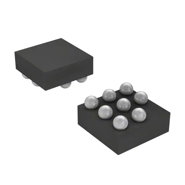
WLP-8-11-N-3D
Description
BGF106C is an ESD protection circuit and filtering interface for SIM cards. All external IOs are protected against
ESD pulses of ±15 kV contact discharge according to IEC61000-4-2. The wafer level package is a green lead-free
and halogen-free package with a size of only 1.2 mm x 1.2 mm and a total height of 0.6 mm
Vcc
C2
RST_int
A3
R1, 100Ω
A2
RST_ext
CLK_int
B3
R2, 47Ω
B1
CLK_ext
Data I/O_int
C3
R3, 100Ω
C1
Data I/O_ext
GND, B2
BGF106_ schematic_app.vsd
Figure 1-1 Schematic Diagram and Package Configuration
Type
Package
Marking
Chip
BGF106C
WLP-8-11
6C
N0727
Final Datasheet
3
Rev. 3.1, 2013-01-16
�BGF106C
Characteristics
2
Characteristics
Table 2-1
Maximum Ratings
Parameter
Symbol
Values
Min.
Typ.
Max.
Unit
Note /
Test Condition
Voltage at all pins to GND
VP
0
–
5.5
V
–
Operating temperature range
TOP
-40
–
+85
°
–
Storage temperature range
TSTG
-65
–
+150
°C
–
Summed up input power for all pins
Pin
–
–
60
mW
TS < 70 °C
Contact discharge at internal pins A3, B3, C3 to VESD
any other pin
-2
–
2
kV
–
Contact discharge at external pins A2, B1, C1, VESD
C2 to GND
-15
–
15
kV
–
Electrostatic discharge according to IEC61000-4-2
Attention: Stresses above the max. values listed here may cause permanent damage to the device.
Exposure to absolute maximum rating conditions for extended periods may affect device
reliability. Maximum ratings are absolute ratings; exceeding only one of these values may
cause irreversible damage to the integrated circuit.
2.1
Electrical Characteristics
Table 2-2
Electrical Characteristics1)
Parameter
Symbol
Values
Min.
Typ.
Max.
Unit
Note /
Test Condition
Resistors R1, R3
R1,3
80
100
120
Ω
–
Resistor R2
R2
37.6
47
56.4
Ω
–
Reverse current of ESD protection diodes
IR
–
–
1
2
100
1000
nA
nA
V=3V
V=5V
Breakdown voltage of ESD diodes
V(BR)
6.5
7.8
–
V
I(BR) = 1 mA
Line capacitance
Capacitance of all lines to GND
1) at TA = 25 °C
CT
–
16.5
20
pF
V=0V
Final Datasheet
4
Rev. 3.1, 2013-01-16
�BGF106C
Typical Characteristics
3
Typical Characteristics
Line B3-B1
Line C3-C1
Line A3-A2
Typical Insertion Loss
0
-5
S21 [dB]
-10
-15
-20
-25
-30
-35
-40
1
10
100
1000
10000
f [MHz]
Figure 3-1 Insertion loss, ZS=ZL=50 Ω
Typical Cross Talk
0
S21 [dB]
-20
-40
-60
-80
-100
-120
1
10
100
1000
10000
f [MHz]
Figure 3-2 Cross talk, ZS=ZL=50 Ω (all unused input and output pins are terminated with 50 Ω)
Final Datasheet
5
Rev. 3.1, 2013-01-16
�BGF106C
Package
Package
Solder balls face up
0.6 ±0.05
B
0.4
(0.2 ±0.05)
C
(0.2 ±0.05)
A3
A2
B3
B2
B1
C3
C2
C1
2 x 0.4 = 0.8
8x
0.08 C
8x
COPLANARITY
ø0.05 M A B
A
1.2 ±0.05
2 x 0.4 = 0.8
0.1 C
0.4
0.2 ±0.05
STANDOFF
SEATING PLANE 3)
Pin A1
2)
Corner Index Area
1.2 ±0.05
(0.2 ±0.05)
Solder balls face down
(0.2 ±0.05)
4
0.25 ±0.04 1)
1) Dimension is measured at the maximum solder ball diameter, parallel to primary datum C
2) A1 corner identified by marking
3) Primary datum C and seating plane are defined by the domed crowns of the balls
WLP-8-11-N-PO V01
Figure 4-1 WLP-8-11 Package outline (dimension in mm)
0.8
0.8
0.4
0.4
0.25
WLP-8-11-N-FP V01
Figure 4-2 WLP-8-11 Footprint (dimension in mm)
4 ±0.1
Pin A1
Corner Index Area
8 ±0.1
1.33 ±0.05
0.25
0.75
1.33 ±0.05
WLP-8-11-N-TP V01
Figure 4-3 WLP-8-11 Packing (dimension in mm)
Final Datasheet
6
Rev. 3.1, 2013-01-16
�w w w . i n f i n e o n . c o m
Published by Infineon Technologies AG
�


 工商网监
湘ICP备2023018690号
工商网监
湘ICP备2023018690号
