BGS12SN6
Wideband RF SPDT Switch in small package with 0.77mm2 footprint
Data Sheet
Revision 2.3, 2016-09-07
Power Management & Multimarket
�Edition September 7, 2016
Published by
Infineon Technologies AG
81726 Munich, Germany
c
2011
Infineon Technologies AG
All Rights Reserved.
Legal Disclaimer
The information given in this document shall in no event be regarded as a guarantee of conditions or characteristics.
With respect to any examples or hints given herein, any typical values stated herein and/or any information regarding
the application of the device, Infineon Technologies hereby disclaims any and all warranties and liabilities of any kind,
including without limitation, warranties of non-infringement of intellectual property rights of any third party.
Information
For further information on technology, delivery terms and conditions and prices, please contact the nearest Infineon
Technologies Office (www.infineon.com).
Warnings
Due to technical requirements, components may contain dangerous substances. For information on the types in
question, please contact the nearest Infineon Technologies Office.
Infineon Technologies components may be used in life-support devices or systems only with the express written
approval of Infineon Technologies, if a failure of such components can reasonably be expected to cause the failure of
that life-support device or system or to affect the safety or effectiveness of that device or system. Life support devices
or systems are intended to be implanted in the human body or to support and/or maintain and sustain and/or protect
human life. If they fail, it is reasonable to assume that the health of the user or other persons may be endangered.
�BGS12SN6
Revision History
Document No.: BGS12SN6.pdf
Previous Version: Revision v2.2 - 2016-08-03
Page
Subjects (major changes since last revision)
9
Update Test conditions of RF input power
Trademarks of Infineon Technologies AG
AURIXTM , C166TM , CanPAKTM , CIPOSTM , CIPURSETM ,CoolGaNTM ,CoolMOSTM , CoolSETTM , CoolSiCTM , CORECONTROLTM ,
DAVETM , DI-POLTM ,EasyPIMTM , EconoBRIDGETM , EconoDUALTM , EconoPACKTM , EconoPIMTM , EiceDRIVERTM , eupecTM ,
FCOSTM , HITFETTM , HybridPACKTM , ISOFACETM , I2 RFTM , IsoPACKTM , MIPAQTM , ModSTACKTM , my-dTM , NovalithICTM ,
OmniTuneTM , OptiMOSTM , ORIGATM , OPTIGATM , PROFETTM , PRO-SILTM , PRIMARIONTM , PrimePACKTM , RASICTM ,
ReverSaveTM , SatRICTM , SIEGETTM , SIPMOSTM , SOLID FLASHTM , SmartLEWISTM , TEMPFETTM , thinQ!TM , TriCoreTM ,
TRENCHSTOPTM .
Other Trademarks
Advance Design SystemTM (ADS) of Agilent Technologies, AMBATM , ARMTM , MULTI-ICETM , PRIMECELLTM , REALVIEWTM ,
THUMBTM of ARM Limited, UK. AUTOSARTM is licensed by AUTOSAR development partnership. BluetoothTM of Bluetooth
SIG Inc. CAT-iqTM of DECT Forum. COLOSSUSTM , FirstGPSTM of Trimble Navigation Ltd. EMVTM of EMVCo, LLC (Visa
Holdings Inc.). EPCOSTM of Epcos AG. FLEXGOTM of Microsoft Corporation. FlexRayTM is licensed by FlexRay Consortium.
HYPERTERMINALTM of Hilgraeve Incorporated. IECTM of Commission Electrotechnique Internationale. IrDATM of Infrared Data
Association Corporation. ISOTM of INTERNATIONAL ORGANIZATION FOR STANDARDIZATION. MATLABTM of MathWorks,
Inc. MAXIMTM of Maxim Integrated Products, Inc. MICROTECTM , NUCLEUSTM of Mentor Graphics Corporation. MifareTM of
NXP. MIPITM of MIPI Alliance, Inc. MIPSTM of MIPS Technologies, Inc., USA. muRataTM of MURATA MANUFACTURING CO.,
MICROWAVE OFFICETM (MWO) of Applied Wave Research Inc., OmniVisionTM of OmniVision Technologies, Inc. OpenwaveTM
Openwave Systems Inc. RED HATTM Red Hat, Inc. RFMDTM RF Micro Devices, Inc. SIRIUSTM of Sirius Sattelite Radio Inc.
SOLARISTM of Sun Microsystems, Inc. SPANSIONTM of Spansion LLC Ltd. SymbianTM of Symbian Software Limited. TAIYO
YUDENTM of Taiyo Yuden Co. TEAKLITETM of CEVA, Inc. TEKTRONIXTM of Tektronix Inc. TOKOTM of TOKO KABUSHIKI
KAISHA TA. UNIXTM of X/Open Company Limited. VERILOGTM , PALLADIUMTM of Cadence Design Systems, Inc. VLYNQTM of
Texas Instruments Incorporated. VXWORKSTM , WIND RIVERTM of WIND RIVER SYSTEMS, INC. ZETEXTM of Diodes Zetex
Limited.
Last Trademarks Update 2012-12-13
Data Sheet
3
Revision 2.3 - 2016-09-07
�BGS12SN6
Contents
1 Features
7
2 Product Description
7
3 Maximum Ratings
9
4 Operation Ranges
9
5 RF Characteristics
10
6 Pin Description
12
7 Package Information
12
Data Sheet
4
Revision 2.3 - 2016-09-07
�BGS12SN6
List of Figures
1
2
3
4
5
6
7
8
9
BGS12SN6 Block Diagram . . . .
Pin Configuration . . . . . . . . . .
Package Outline (TSNP-6-2) . . .
Package Outline (TSNP-6-8) . . .
Footprint (TSNP-6-2/-8) . . . . . .
Pin 1 Marking (TSNP-6-2 top view)
Pin 1 Marking (TSNP-6-8 top view)
Tape Drawing (TSNP-6-2) . . . . .
Tape Drawing (TSNP-6-8) . . . . .
Data Sheet
.
.
.
.
.
.
.
.
.
.
.
.
.
.
.
.
.
.
.
.
.
.
.
.
.
.
.
.
.
.
.
.
.
.
.
.
.
.
.
.
.
.
.
.
.
.
.
.
.
.
.
.
.
.
.
.
.
.
.
.
.
.
.
.
.
.
.
.
.
.
.
.
5
.
.
.
.
.
.
.
.
.
.
.
.
.
.
.
.
.
.
.
.
.
.
.
.
.
.
.
.
.
.
.
.
.
.
.
.
.
.
.
.
.
.
.
.
.
.
.
.
.
.
.
.
.
.
.
.
.
.
.
.
.
.
.
.
.
.
.
.
.
.
.
.
.
.
.
.
.
.
.
.
.
.
.
.
.
.
.
.
.
.
.
.
.
.
.
.
.
.
.
.
.
.
.
.
.
.
.
.
.
.
.
.
.
.
.
.
.
.
.
.
.
.
.
.
.
.
.
.
.
.
.
.
.
.
.
.
.
.
.
.
.
.
.
.
.
.
.
.
.
.
.
.
.
.
.
.
.
.
.
.
.
.
.
.
.
.
.
.
.
.
.
.
.
.
.
.
.
.
.
.
.
.
.
.
.
.
.
.
.
.
.
.
.
.
.
.
.
.
.
.
.
.
.
.
.
.
.
.
.
.
.
.
.
.
.
.
.
.
.
.
.
.
.
.
.
.
.
.
.
.
.
.
.
.
.
.
.
.
.
.
.
.
.
.
.
.
.
.
.
.
.
.
.
.
.
.
.
.
.
.
.
.
.
.
.
.
.
.
.
.
8
12
13
13
14
14
14
15
15
Revision 2.3 - 2016-09-07
�BGS12SN6
List of Tables
1
2
3
4
5
6
7
8
Ordering Information
Truth Table . . . . .
Maximum Ratings .
Operation Ranges .
RF Input Power . . .
RF Characteristics .
Pin Description . . .
Mechanical Data . .
Data Sheet
.
.
.
.
.
.
.
.
.
.
.
.
.
.
.
.
.
.
.
.
.
.
.
.
.
.
.
.
.
.
.
.
.
.
.
.
.
.
.
.
.
.
.
.
.
.
.
.
.
.
.
.
.
.
.
.
.
.
.
.
.
.
.
.
.
.
.
.
.
.
.
.
.
.
.
.
.
.
.
.
.
.
.
.
.
.
.
.
.
.
.
.
.
.
.
.
.
.
.
.
.
.
.
.
.
.
.
.
.
.
.
.
.
.
.
.
.
.
.
.
.
.
.
.
.
.
.
.
6
.
.
.
.
.
.
.
.
.
.
.
.
.
.
.
.
.
.
.
.
.
.
.
.
.
.
.
.
.
.
.
.
.
.
.
.
.
.
.
.
.
.
.
.
.
.
.
.
.
.
.
.
.
.
.
.
.
.
.
.
.
.
.
.
.
.
.
.
.
.
.
.
.
.
.
.
.
.
.
.
.
.
.
.
.
.
.
.
.
.
.
.
.
.
.
.
.
.
.
.
.
.
.
.
.
.
.
.
.
.
.
.
.
.
.
.
.
.
.
.
.
.
.
.
.
.
.
.
.
.
.
.
.
.
.
.
.
.
.
.
.
.
.
.
.
.
.
.
.
.
.
.
.
.
.
.
.
.
.
.
.
.
.
.
.
.
.
.
.
.
.
.
.
.
.
.
.
.
.
.
.
.
.
.
.
.
.
.
.
.
.
.
.
.
.
.
.
.
.
.
.
.
.
.
.
.
.
.
.
.
.
.
.
.
.
.
.
.
.
.
.
.
.
.
.
.
.
.
.
.
.
.
.
.
.
.
.
.
.
.
7
8
9
9
9
10
12
12
Revision 2.3 - 2016-09-07
�BGS12SN6
BGS12SN6 Wideband RF SPDT Switch in small package with 0.77mm2
footprint
1 Features
• 2 high-linearity TRx paths with power handling capability of up to
30 dBm
• High switching speed, ideal for WLAN and Bluetooth applications
• All ports fully bi-directional
• Low insertion loss
• Low harmonic generation
• High port-to-port-isolation
• 0.05 to 6 GHz coverage
• High ESD robustness
• On-chip control logic
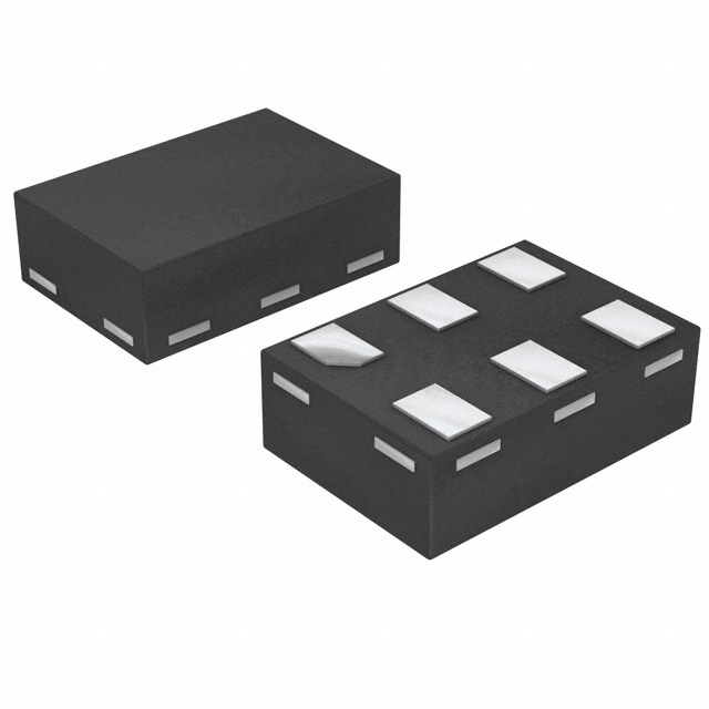
• Very small leadless and halogen free package TSNP-6-2(-8)
(0.7x1.1 mm2 ) with super low height of 0.375 mm
• No decoupling capacitors required if no DC applied on RF lines
• RoHS compliant package
2 Product Description
The BGS12SN6 RF MOS switch is specifically designed for WLAN and Bluetooth applications. Any of the 2 ports
can be used as termination of the diversity antenna handling up to 30 dBm.
This single supply chip integrates on-chip CMOS logic driven by a simple, single-pin CMOS or TTL compatible
control input signal. The 0.1 dB compression point exceeds the switch’s maximum input power level, resulting in
linear performance at all signal levels. The RF switch has a very low insertion loss of 0.25 dB in the 1 GHz and 0.29
dB in the 2.5 GHz range.
Unlike GaAs technology, external DC blocking capacitors at the RF ports are only required if DC voltage is applied
externally.
The BGS12SN6 RF switch is manufactured in Infineon’s patented MOS technology, offering the performance of GaAs
with the economy and integration of conventional CMOS including the inherent higher ESD robustness.
The device has a very small size of only 0.7x1.1mm2 and a maximum height of 0.375 mm.
Table 1: Ordering Information
Type
Package
Marking
BGS12SN6
TSNP-6-2/-8
T
Data Sheet
7
Revision 2.3 - 2016-09-07
�BGS12SN6
RFin
BGS12SN6
RF1
RF2
SPDT
DGND
Ctrl
VDD
Decoder + ESD
Protection
Figure 1: BGS12SN6 Block Diagram
Table 2: Truth Table
Switched Paths
Ctrl
RFin - RF1
0
RFin - RF2
1
Data Sheet
8
Revision 2.3 - 2016-09-07
�BGS12SN6
3 Maximum Ratings
Table 3: Maximum Ratings at TA = 25 ◦ C, unless otherwise specified
Parameter
Symbol
Values
Min.
Typ.
Max.
Unit
Note / Test Condition
Supply Voltage
Vdd
-0.5
–
3.6
V
–
Maximum DC-Voltage on Other Pins
VDC
0
–
0
V
No external DC voltage
◦
allowed
Storage Temperature Range
TSTG
-65
–
150
RF Input Power
PRF
–
–
32
Junction Temperature
C
–
dBm
CW, 50 Ohm
Tj
–
–
125
◦
VESD_HBM
−1000
–
+1000
V
–
VESD_RFin
−8
–
+8
kV
RFin versus GND, with
–
C
ESD Capability
Human Body Model 1)
ESD Capability RFin Port
2)
27 nH shunt inductor
1)
Human Body Model ANSI/ESDA/JEDEC JS-001-2012 (R = 1.5 kΩ, C = 100 pF).
2) IEC 61000-4-2 (R = 330 Ω, C = 150 pF), contact discharge.
Attention:
Stresses above the max. values listed here may cause permanent damage to the device. Exposure to absolute maximum rating conditions for extended periods may affect device reliability. Maximum ratings are
absolute ratings; exceeding only one of these values may cause irreversible damage to the integrated circuit.
4 Operation Ranges
Table 4: Operation Ranges
Parameter
Symbol
Values
Unit
Min.
Typ.
Max.
◦
Note / Test Condition
Ambient Temperature
TA
-40
25
85
C
–
RF Frequency
f
0.1
–
6
GHz
–
Supply Voltage
Vdd
1.8
–
3.5
V
–
Control Voltage Low
VCtrl_L
-0.3
–
0.43
V
–
Control Voltage High
VCtrl_H
1.35
–
VDD
V
–
Table 5: RF Input Power
Parameter
RF Input Power (50Ω)
Data Sheet
Symbol
PIn
Values
Min.
Typ.
Max.
–
–
30
9
Unit
Note / Test Condition
dBm
CW, 50 Ohm
Revision 2.3 - 2016-09-07
�BGS12SN6
5 RF Characteristics
Table 6: RF Characteristics
Test Conditions (unless otherwise specified):
• Terminating port impedance: Z0 = 50 Ω
• Temperature range: TA = -40 ... +85 ◦ C
• Supply voltage: VDD = 1.8 ... 3.4 V
• Input power: PIN = 0 dBm
Parameter
Symbol
Values
Unit
Note / Test Condition
0.42
dB
699-824 MHz
0.25
0.43
dB
824-915 MHz
0.28
0.45
dB
1710-1910 MHz
–
0.29
0.50
dB
2170-2690 MHz
–
0.53
0.78
dB
5000 MHz
–
0.65
0.90
dB
6000 MHz
–
0.23
0.35
dB
699-824 MHz
–
–
0.25
0.28
0.35
0.40
dB
dB
824-915 MHz
1710-1910 MHz
–
0.29
0.45
dB
2170-2690 MHz
–
0.53
0.70
dB
5000 MHz
–
0.65
0.85
dB
6000 MHz
22
30
–
dB
699-824 MHz
22
30
–
dB
824-915 MHz
20
25
–
dB
1710-1910 MHz
17
20
–
dB
2170-2690 MHz
12
18
–
dB
5000 MHz
12
16
–
dB
6000 MHz
Min.
Typ.
Max.
–
0.23
–
–
Insertion Loss
All RF Ports
IL
1
Insertion Loss
All RF Ports
IL
Return Loss
All RF Ports
1
RL
TA = +25 ◦ C, VDD = 2.6 V
Data Sheet
10
Revision 2.3 - 2016-09-07
�BGS12SN6
Parameter
Symbol
Values
Unit
Note / Test Condition
Min.
Typ.
Max.
36
42
–
dB
699-824 MHz
35
40
–
dB
824-915 MHz
28
32
–
dB
1710-1910 MHz
26
28
–
dB
2170-2690 MHz
15
19
–
dB
5000 MHz
15
18
–
dB
6000 MHz
43
47
–
dB
699-824 MHz
42
45
–
dB
824-915 MHz
34
38
–
dB
1710-1910 MHz
30
33
–
dB
2170-2690 MHz
18
21
–
dB
5000 MHz
18
21
–
dB
6000 MHz
–
-80
-75
dBc
VDD = 2.85V , TA = 25 ◦ C,
–
-87
-80
dBc
f
Isolation
RFin to RF1/RF2 Port
RF1 to RF2 Port /
RF2 to RF1 Port
ISORFin−RFx
ISOPort−Port
Harmonic Generation up to 12.75 GHz
All RF Ports, 2nd Harmonic
All RF Ports, 3rd Harmonic
PHarm
=
824 MHz,
Pin
=
27.5 dBm, 50 % duty cycle,
50Ω
Compression Point 0.1dB
P0.1dB
P0.1dB
–
–
34
dBm
–
Intermodulation Distortion in Rx Band
IMD2
IMD2
–
-110
-100
dBm
Tx = 10 dBm, Interferer = -15
IMD3
IMD3
–
-130
-120
dBm
dBm, 50Ω
Switching Time and Current Consumption
RF Rise Time
t10%−90%
–
60
100
ns
10% - 90% of RF Signal
Ctrl to RF Time
tCtrl−RF
–
400
500
ns
50% of Ctrl Signal to 90% of
RF Signal
Power Up Settling Time
tPUP
–
5
15
µs
After power down
Supply Current
Idd
–
100
180
µA
–
Control Current
ICtrl
–
1
10
µA
–
Note: All electrical characteristics are measured with all RF ports terminated by 50 Ω loads.
Data Sheet
11
Revision 2.3 - 2016-09-07
�BGS12SN6
6 Pin Description
Figure 2: Pin Configuration
Table 7: Pin Description
Pin No.
Name
Pin
Buffer
Type
Type
Function
1
RF2
I/O
RF Port 2
2
GND
GND
Ground
3
RF1
I/O
RF Port 1
4
Vdd
PWR
Supply Voltage
5
RFin
I/O
RF Port In
6
CTRL
I
Control Pin
7 Package Information
Table 8: Mechanical Data
Parameter
Symbol
Value
Unit
X-Dimension
X
0.7 ± 0.05
mm
Y-Dimension
Y
1.1 ± 0.05
mm
Size
Size
0.77
mm2
Height
H
0.375 +0.025/−0.025
mm
Data Sheet
12
Revision 2.3 - 2016-09-07
�BGS12SN6
Bottom view
0.7 ±0.05
0.2 ±0.05 1)
0.02 MAX.
0.8 ±0.05
3
2
1
4
5
6
1.1 ±0.05
+0.025
0.375 -0.015
0.2 ±0.05 1)
Top view
0.4 ±0.05
Pin 1 marking
1) Dimension applies to plated terminals
TSNP-6-2-PO V01
Figure 3: Package Outline (TSNP-6-2)
Bottomaview
0.7 ±0.05
A
0.1 A
3
2
0.4
2axa 0.4a =a 0.8
0.2 ±0.05
6x
Pina1amarking
1
0.4
4
5
6
6x
1.1 ±0.05
0.03aMAX.
STANDOFF
0.1 B
0.375 ±0.025
0.2 ±0.05
Topaview
B
TSNP-6-8-POa V03
Figure 4: Package Outline (TSNP-6-8)
Data Sheet
13
Revision 2.3 - 2016-09-07
�BGS12SN6
NSMD
0.4
0.4
0.25
0.25
0.4
0.4
0.25
0.25
(stencilmthicknessm100mµm)
Copper
Stencilmapertures
Soldermmask
TSNP-6-2/-8-FPmV01
Figure 5: Footprint (TSNP-6-2/-8)
1
Type code
Monthly data code
Pin 1 marking
TSNP-6-2-MK V01
Figure 6: Pin 1 Marking (TSNP-6-2 top view)
1
Type code
Monthly data code
Pin 1 marking
TSNP-6-8-MK V02
Figure 7: Pin 1 Marking (TSNP-6-8 top view)
Data Sheet
14
Revision 2.3 - 2016-09-07
�BGS12SN6
1.25
Pin 1
marking
8
0.5
2
0.85
TSNP-6-2-TP V01
Figure 8: Tape Drawing (TSNP-6-2)
1.25
Pin 1
marking
8
0.49
2
0.85
TSNP-6-8-TP V01
Figure 9: Tape Drawing (TSNP-6-8)
Data Sheet
15
Revision 2.3 - 2016-09-07
�w w w . i n f i n e o n . c o m
Published by Infineon Technologies AG
�


 工商网监
湘ICP备2023018690号
工商网监
湘ICP备2023018690号
