BGS13S4N9
Wideband RF SP3T Switch
Data Sheet
Revision 1.0 - 2016-04-12
Final
Power Management & Multimarket
�Edition 2016-04-12
Published by Infineon Technologies AG
81726 Munich, Germany
c
2016
Infineon Technologies AG
All Rights Reserved.
LEGAL DISCLAIMER
The information given in this document shall in no event be regarded as a guarantee of conditions or characteristics.
With respect to any examples or hints given herein, any typical values stated herein and/or any information regarding
the application of the device, Infineon Technologies hereby disclaims any and all warranties and liabilities of any kind,
including without limitation, warranties of non-infringement of intellectual property rights of any third party.
Information
For further information on technology, delivery terms and conditions and prices, please contact the nearest Infineon
Technologies Office (www.infineon.com).
Warnings
Due to technical requirements, components may contain dangerous substances. For information on the types in
question, please contact the nearest Infineon Technologies Office. Infineon Technologies components may be used
in life-support devices or systems only with the express written approval of Infineon Technologies, if a failure of such
components can reasonably be expected to cause the failure of that life-support device or system or to affect the
safety or effectiveness of that device or system. Life support devices or systems are intended to be implanted in
the human body or to support and/or maintain and sustain and/or protect human life. If they fail, it is reasonable to
assume that the health of the user or other persons may be endangered.
�BGS13S4N9
Confidential
Revision History
Document No.: BGS13S4N9_Final_v1.0.pdf
Revision History: Final Rev. v1.0
Previous Version: Target, Revision v1.0 - 2015-10-21
Page
Subjects (major changes since last revision)
Trademarks of Infineon Technologies AG
TM
TM
TM
TM
TM
TM
TM
TM
TM
TM
TM
µHVIC , µIPM , µPFC , AU-ConvertIR , AURIX , C166 , CanPAK , CIPOS , CIPURSE , CoolDP , CoolGaN ,
TM
TM
TM
TM
TM
TM
TM
TM
TM
TM
COOLiR , CoolMOS , CoolSET , CoolSiC , DAVE , DI-POL , DirectFET , DrBlade , EasyPIM , EconoBRIDGE ,
TM
TM
TM
TM
TM
TM
TM
TM
TM
EconoDUAL , EconoPACK , EconoPIM , EiceDRIVER , eupec , FCOS , GaNpowIR , HEXFET , HITFET ,
TM
TM
TM
TM
TM
TM
TM
TM
TM
TM
HybridPACK , iMOTION , IRAM , ISOFACE , IsoPACK , LEDrivIR , LITIX , MIPAQ , ModSTACK , my-d ,
TM
TM
TM
TM
TM
TM
TM
TM
TM
NovalithIC , OPTIGA , OptiMOS , ORIGA , PowIRaudio , PowIRStage , PrimePACK , PrimeSTACK , PROFET ,
TM
TM
TM
TM
TM
TM
TM
TM
TM
PRO-SIL , RASIC , REAL3 , SmartLEWIS , SOLID FLASH , SPOC , StrongIRFET , SupIRBuck , TEMPFET ,
TM
TM
TM
TM
TM
TRENCHSTOP , TriCore , UHVIC , XHP , XMC .
Other Trademarks
All referenced product or service names and trademarks are the property of their respective owners.
Trademarks updated November 2015
Data Sheet
3
Revision 1.0 - 2016-04-12
�BGS13S4N9
Confidential
Contents
Contents
1 Features
5
2 Product Description
5
3 Maximum Ratings
6
4 Operation Ranges
7
5 RF Characteristics
8
6 GPIO Specification
10
7 Pin Definition and Package Outline
10
List of Figures
1
2
3
4
5
6
BGS13S4N9 Block Diagram . . . . . . . . . . . . . . .
Pin out (top view) . . . . . . . . . . . . . . . . . . . . .
Package Outline (bottom and side view) . . . . . . . .
Land pattern and stencil mask . . . . . . . . . . . . .
Marking Pattern . . . . . . . . . . . . . . . . . . . . . .
Tape and Reel (Reel φ 180 mm: 15.000 Pieces/Reel) .
.
.
.
.
.
.
.
.
.
.
.
.
.
.
.
.
.
.
.
.
.
.
.
.
.
.
.
.
.
.
.
.
.
.
.
.
.
.
.
.
.
.
.
.
.
.
.
.
.
.
.
.
.
.
.
.
.
.
.
.
.
.
.
.
.
.
.
.
.
.
.
.
.
.
.
.
.
.
.
.
.
.
.
.
.
.
.
.
.
.
.
.
.
.
.
.
.
.
.
.
.
.
.
.
.
.
.
.
.
.
.
.
.
.
.
.
.
.
.
.
.
.
.
.
.
.
.
.
.
.
.
.
.
.
.
.
.
.
.
.
.
.
.
.
.
.
.
.
.
.
.
.
.
.
.
.
.
.
.
.
.
.
6
10
11
11
12
13
.
.
.
.
.
.
.
.
.
.
.
.
.
.
.
.
.
.
.
.
.
.
.
.
.
.
.
.
.
.
.
.
.
.
.
.
.
.
.
.
.
.
.
.
.
.
.
.
.
.
.
.
.
.
.
.
.
.
.
.
.
.
.
.
.
.
.
.
.
.
.
.
.
.
.
.
.
.
.
.
.
.
.
.
.
.
.
.
.
.
.
.
.
.
.
.
.
.
.
.
.
.
.
.
.
.
.
.
.
.
.
.
.
.
.
.
.
.
.
.
.
.
.
.
.
.
.
.
.
.
.
.
.
.
.
.
.
.
.
.
.
.
.
.
.
.
.
.
.
.
.
.
.
.
.
.
.
.
.
.
.
.
.
.
.
.
.
.
.
.
.
.
.
.
.
.
.
.
.
.
.
.
.
.
.
.
.
.
.
.
.
.
.
.
.
.
.
.
.
.
.
.
.
.
.
.
.
.
.
.
.
.
.
.
.
.
.
.
.
.
.
.
.
.
.
.
.
.
.
.
.
.
.
.
.
.
.
.
.
.
.
.
.
.
.
.
.
.
.
.
.
.
.
.
.
.
.
.
.
.
.
.
.
.
.
.
.
.
.
.
.
.
.
.
.
.
.
.
.
.
.
.
.
.
.
.
.
.
.
.
.
.
.
.
.
.
.
.
.
.
.
.
.
.
.
.
.
.
.
.
.
.
.
.
.
.
.
.
.
.
.
.
.
.
5
6
7
7
7
8
9
10
10
11
12
12
List of Tables
1
2
3
4
5
6
7
8
9
10
11
12
Ordering Information . . . .
Maximum Ratings, Table I .
Maximum Ratings, Table II .
Operation Ranges . . . . .
RF Input Power . . . . . . .
RF Characteristics . . . . .
RF Characteristics . . . . .
GPIO Truth Table . . . . . .
Pin Configuration . . . . . .
Mechanical Data . . . . . .
Year Date Code . . . . . . .
Week Date Code . . . . . .
Data Sheet
.
.
.
.
.
.
.
.
.
.
.
.
.
.
.
.
.
.
.
.
.
.
.
.
.
.
.
.
.
.
.
.
.
.
.
.
.
.
.
.
.
.
.
.
.
.
.
.
.
.
.
.
.
.
.
.
.
.
.
.
.
.
.
.
.
.
.
.
.
.
.
.
.
.
.
.
.
.
.
.
.
.
.
.
.
.
.
.
.
.
.
.
.
.
.
.
.
.
.
.
.
.
.
.
.
.
.
.
.
.
.
.
.
.
.
.
.
.
.
.
.
.
.
.
.
.
.
.
.
.
.
.
.
.
.
.
.
.
.
.
.
.
.
.
4
.
.
.
.
.
.
.
.
.
.
.
.
.
.
.
.
.
.
.
.
.
.
.
.
.
.
.
.
.
.
.
.
.
.
.
.
Revision 1.0 - 2016-04-12
�BGS13S4N9
Confidential
BGS13S4N9 Wideband RF SP3T Switch
1 Features
• 3 high-linearity TRx paths with power handling capability of up to
30 dBm
• Low insertion loss
• Low harmonic generation
• High port-to-port-isolation
• Suitable for Edge / CDMA2000 / LTE / WCDMA applications
• 0.1 to 3.0 GHz coverage
• No decoupling capacitors required if no DC applied on RF lines
• On-chip control logic including ESD protection
• General Purpose Input-Output (GPIO) Interface
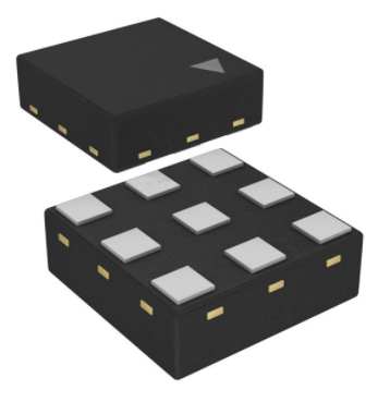
• Small form factor 1.1 mm x 1.1 mm x 0.375 mm
• No power supply blocking required
• High EMI robustness
• RoHS and WEEE compliant package
2 Product Description
The BGS13S4N9 RF MOS switch is specifically designed for cell phone and mobile applications. Any of the 3 ports
can be used as termination of the diversity antenna handling up to 30 dBm.
This SP3T offers low insertion loss and high robustness against interferer signals at the antenna port and low
harmonic generation in termination mode. The on-chip controller integrates CMOS logic and level shifters, driven
by control inputs from 1.35 V to VDD . The BGS13S4N9 RF Switch is manufactured in Infineon’s patented MOS
technology, offering the performance of GaAs with the economy and integration of conventional CMOS including the
inherent higher ESD robustness. The device has a very small size of only 1.1 x 1.1 mm2 and a maximum height of
0.375 mm.
No decoupling capacitors are required in typical applications as long as no DC is applied to any RF port.
Table 1: Ordering Information
Type
Package
Marking
BGS13S4N9
TSNP-9-3
W
Data Sheet
5
Revision 1.0 - 2016-04-12
�BGS13S4N9
Confidential
RFin
BGS13S4N9
RF2
RF1
RF3
SP3T
DGND
VDD
V2
V1
Decoder + ESD
Pr otection
Figure 1: BGS13S4N9 Block Diagram
3 Maximum Ratings
Stresses above the maximum values listed here may cause permanent damage to the device. Exposure to absolute
maximum rating conditions for extended periods may affect device reliability. Maximum ratings are absolute ratings;
exceeding only one of these values may cause irreversible damage to the integrated circuit.
Table 2: Maximum Ratings, Table I at TA = 25 ◦C, unless otherwise specified
Parameter
Symbol
Values
Min.
Typ.
Max.
Unit
Note / Test Condition
Frequency Range
f
0.1
–
3.0
GHz
1)
Supply voltage
VDD
-0.5
–
3.6
V
–
150
◦
C
–
C
–
Storage temperature range
TSTG
-55
–
Junction temperature
Tj
–
–
125
◦
RF input power at all Rx ports
PRF_Rx
–
–
32
dBm
CW
2)
VESD_CDM
-1000
–
+1000
V
All pins
3)
VESD_HBM
-1000
–
+1000
V
All pins excluding RFin
-1000
–
+1000
V
RFin vs. other pins
-8000
–
+8000
V
ANT versus system GND,
ESD capability, CDM
ESD capability, HBM
4)
ESD capability, system level
VESD_ANT
with 16 nH shunt inductor
Type LQW15AN16NG80
1) There
is also a DC connection between switched paths. The DC voltage at RF ports VRFDC has to be 0V.
2) Field-Induced Charged-Device Model JESD22-C101. Simulates charging/discharging events that occur in production equipment and
processes. Potential for CDM ESD events occurs whenever there is metal-to-metal contact in manufacturing.
3) Human Body Model ANSI/ESDA/JEDEC JS-001-2012 (R=1.5 kΩ, C=100 pF).
4) IEC 61000-4-2 (R=330 Ω, C=150 pF), contact discharge.
Data Sheet
6
Revision 1.0 - 2016-04-12
�BGS13S4N9
Confidential
Table 3: Maximum Ratings, Table II at TA = 25 ◦C, unless otherwise specified
Parameter
Symbol
Maximum DC-voltage on RF-
VRFDC
Values
Min.
Typ.
Max.
0
–
0
Unit
Note / Test Condition
V
No DC voltages allowed on
Ports and RF-Ground
RF-Ports
4 Operation Ranges
Table 4: Operation Ranges
Parameter
Symbol
Values
Unit
Note / Test Condition
3.3
V
–
80
150
µA
–
1.35
–
VDD
V
–
VCtrl_L
-0.3
–
0.43
V
–
CCtrl
–
–
2
pF
–
TA
-40
25
85
◦
–
Min.
Typ.
Max.
VDD
1.8
–
Supply current
IDD
–
GPIO control voltage high
VCtrl_H
GPIO control voltage low
GPIO control input capaci-
Supply voltage
1)
tance
Ambient temperature
1) T
C
◦
◦
A = −40 C - 85 C, VDD= 1.8 - 3.3 V
Table 5: RF Input Power
Parameter
Rx ports (50 Ω)
Data Sheet
Symbol
PRF_Rx
Values
Min.
Typ.
Max.
–
–
30
7
Unit
Note / Test Condition
dBm
–
Revision 1.0 - 2016-04-12
�BGS13S4N9
Confidential
5 RF Characteristics
Table 6: RF Characteristics at TA = −40 ◦C–85 ◦C, PIN = 0 dBm, Supply Voltage VDD= 1.8 V–3.3 V, Z0 = 50 Ohm,
unless otherwise specified
Parameter
Symbol
Values
Unit
Note / Test Condition
Min.
Typ.
Max.
0.10
0.20
0.25
dB
824–915 MHz
0.20
0.30
0.40
dB
1710–1910 MHz
0.25
0.40
0.60
dB
2170–2500 MHz
0.40
0.55
0.65
dB
2700MHz
0.15
0.20
0.25
dB
824–915 MHz
0.25
0.30
0.35
dB
1710–1910 MHz
0.35
0.40
0.50
dB
2170–2500 MHz
0.50
0.55
0.65
dB
2700MHz
28
31
33
dB
824–915 MHz
18
20
24
dB
1710–1910 MHz
15
18
20
dB
2170–2500 MHz
13
14
16
dB
2700MHz
31
33
–
dB
824–915 MHz
23
27
–
dB
1710–1910 MHz
17
22
–
dB
2170–2500 MHz
16
21
–
dB
2700MHz
32
34
–
dB
824–915 MHz
21
25
–
dB
1710–1910 MHz
17
23
–
dB
2170–2500 MHz
15
19
–
dB
2700MHz
Insertion Loss
All Rx Ports
IL
1)
Insertion Loss
All Rx Ports
IL
Return Loss
All Rx Ports
RL
1)
Isolation
RFin to RF1/RF2/RF32)
ISOIn-RFx
RF1 to RF2 / RF2 to RF13)
RF1 to RF3 / RF3 to RF14)
RF2 to RF3 / RF3 to RF25)
1) T
ISOport-port
◦
A = 25 C, VDD = 3V
2) Any
RF Port ON
ON
4) RF3 ON
5) RF2 ON
3) RF1
Data Sheet
8
Revision 1.0 - 2016-04-12
�BGS13S4N9
Confidential
Table 7: RF Characteristics at TA = −40 ◦C–85 ◦C, PIN = 0 dBm, Supply Voltage VDD= 1.8 V–3.3 V, Z0 = 50 Ohm,
unless otherwise specified
Parameter
Symbol
Values
Unit
Note / Test Condition
–
dBm
698–960 MHz
Min.
Typ.
Max.
34
–
P0.1 dB Compression Point, Extrapolated
All Rx Ports
P0.1dB
Harmonic Generation up to 12.75 GHz
H2
PHarm
–
-80
-70
dBc
27 dBm, 50 Ω, CW mode
H3
PHarm
–
-80
-70
dBc
27 dBm, 50 Ω, CW mode
Intermodulation Distortion in Rx Band1) (TA = 25 ◦C)
IMD2
IMD2
–
-110
-100
dBm
Tx = 10 dBm,
IMD3
IMD3
–
-115
-100
dBm
Interferer = −15 dBm, 50 Ω
RF Rise Time
ton/off
–
0.085
–
µs
Ctrl to RF Time
tCtrl-RF
–
0.55
–
µs
Switching Time
1) With
10 % to 90 % RF ON;
90 % to 10 % RF OFF
50 % of Ctrl Signal to
90 % of RF Signal
external shunt inductor
Data Sheet
9
Revision 1.0 - 2016-04-12
�BGS13S4N9
Confidential
6 GPIO Specification
Table 8: Modes of Operation Truth Table
Control Inputs
State
Mode
V1
V2
RF1
RF2
RF3
1
Isolation
0
0
off
off
off
2
RFin - RF1
1
0
on
off
off
3
RFin - RF2
0
1
off
on
off
4
RFin - RF3
1
1
off
off
on
7 Pin Definition and Package Outline
Table 9: Pin Configuration
No Name
1
V1
2
RF3
3
RF1
4
RFin
5
RF2
6
DGND
7
VDD
8
V2
9
GND
Pin Type
I
I/O
I/O
I/O
I/O
GND
PWR
I
GND
Buffer Type
Function
Control Pin 1
RF-Port3
RF-Port1
RF-Input
RF-Port2
Digital Ground
Power Supply
Control Pin 2
Ground
1
V1
8
V2
7
VDD
2
RF3
9
GND
6
DGND
3
RF1
4
RFin
5
RF2
Figure 2: Pin out (top view)
Data Sheet
10
Revision 1.0 - 2016-04-12
�BGS13S4N9
Confidential
Table 10: Mechanical Data
Parameter
Symbol
Value
Unit
X-Dimension
X
1.1 ± 0.05
mm
Y-Dimension
Y
1.1 ± 0.05
mm
Size
Size
1.21
mm2
Height
H
0.375 ± 0.025
mm
0.4
mm
Pad-Pitch
Figure 3: Package Outline (bottom and side view)
0.4
0.4
0.25
0.4
0.4
0.4
0.25
Optionalksolderkmaskkdam
Copper
Stencilkapertures
Solderkmask
TSNP-9-3-FPkV01
Figure 4: Land pattern and stencil mask
Data Sheet
11
Revision 1.0 - 2016-04-12
�BGS13S4N9
Confidential
Figure 5: Marking Pattern
Table 11: Year date code marking - digit "Y"
Year
"Y"
Year
"Y"
Year
"Y"
2000
0
2010
0
2020
0
2001
1
2011
1
2021
1
2002
2
2012
2
2022
2
2003
2004
3
4
2013
2014
3
4
2023
2024
3
4
2005
5
2015
5
2025
5
2006
6
2016
6
2026
6
2007
7
2017
7
2027
7
2008
8
2018
8
2028
8
2009
9
2019
9
2029
9
Table 12: Week date code marking - digit "W"
Data Sheet
Week
"W"
Week
"W"
Week
"W"
Week
"W"
Week
"W"
1
A
12
N
23
4
34
h
45
v
2
B
13
P
24
5
35
j
46
x
3
C
14
Q
25
6
36
k
47
y
4
D
15
R
26
7
37
l
48
z
5
E
16
S
27
a
38
n
49
8
6
F
17
T
28
b
39
p
50
9
7
G
18
U
29
c
40
q
51
2
8
H
19
V
30
d
41
r
52
3
9
J
20
W
31
e
42
s
10
11
K
L
21
22
Y
Z
32
33
f
g
43
44
t
u
12
Revision 1.0 - 2016-04-12
�BGS13S4N9
Confidential
1.25
Pin 1
marking
8
0.5
2
1.25
TSNP-9-3-TP V01
Figure 6: Tape and Reel (Reel φ 180 mm: 15.000 Pieces/Reel)
Data Sheet
13
Revision 1.0 - 2016-04-12
�w w w . i n f i n e o n . c o m
Published by Infineon Technologies AG
�